The 10 nanometer (10 nm) lithography process is a full node semiconductor manufacturing process following the 14 nm process stopgap. The term "10 nm" is simply a commercial name for a generation of a certain size and its technology, as opposed to gate length or half pitch. Commercial mass production of integrated circuit manufacturing using 10 nm process begun with risk production in late 2016 and ramped up in mid-to-late 2017. This technology is set to be replaced by 7 nm process 2019.
Contents
Industry
Announced during Intel's Technology and Manufacturing Day 2017, Intel's 10 nm process (P1274) is the first high-volume manufacturing process to employ Self-Aligned Quad Patterning (SAQP) with production starting in the second half of 2017. Samsung, which unlike Intel uses LELELE (litho-etch-litho-etch-litho-etch), plans ramp up mass production in May of 2017.
Due to marketing names the transistor sizes vary considerably between leading manufactures. For example, Intel's 10nm process is denser and smaller than TSMC's 7 nm process while Samsung's 10 nm process is more similar to Intel's 14 nm process.
| Fab |
|---|
| Process Name |
| 1st Production |
| Transistor |
| |
| Fin Pitch |
| Fin Width |
| Fin Height |
| Contacted Gate Pitch |
| Interconnect Pitch (M1P) |
| SRAM bit cell (HP) |
| SRAM bit cell (HD) |
| SRAM bit cell (LV) |
| Intel | Samsung | TSMC | SK Hynix | ||||
|---|---|---|---|---|---|---|---|
| P1274 | 10LPE 1st generation; 10 nm Low Power Early , 10LPP2nd generation; 10 nm Low Power Performance , 10LPU3rd generation; 10 nm Low Power Ultimate |
||||||
| 2017 | 2017 | 2017 | 2017 | ||||
| FinFET | |||||||
| Value | 14 nm Δ | Value | 14 nm Δ | Value | 16 nm Δ | Value | 18 nm Δ |
| 34 nm | 0.81x | ? nm | ?x | ? nm | ?x | ? nm | ?x |
| ? nm | ?x | ? nm | ?x | ? nm | ?x | ? nm | ?x |
| 53 nm | 1.26x | ? nm | ?x | ? nm | ?x | ? nm | ?x |
| 54 nm | 0.77x | 64 nm | 0.82x | 64 nm | 0.71x | ? nm | ?x |
| 36 nm | 0.69x | 48 nm | 0.75x | 42 nm | 0.66x | ? nm | ?x |
| 0.0441 µm² | 0.75x | 0.049 µm² | 0.61x | ? µm² | ?x | ? nm | ?x |
| 0.0367 µm² | 0.62x | 0.040 µm² | 0.63x | ? µm² | ?x | ? nm | ?x |
| 0.312 µm² | ?x | ? µm² | ?x | ? µm² | ?x | ? nm | ?x |
Samsung
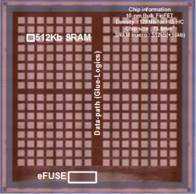
Samsung demonstrated their 128 Mebibit SRAM wafer from their 10nm FinFET process.
| Samsung 128 Mib SRAM demo 10 nm wafer | |||||||||||||||
|---|---|---|---|---|---|---|---|---|---|---|---|---|---|---|---|
|

| ||||||||||||||
10 nm Microprocessors
- MediaTek
- Qualcomm
- Xiaomi
This list is incomplete; you can help by expanding it.
10 nm Microarchitectures
- Intel
- Qualcomm
This list is incomplete; you can help by expanding it.
Documents
References
- Cho, H-J., et al. "Si FinFET based 10nm technology with multi Vt gate stack for low power and high performance applications." VLSI Technology, 2016 IEEE Symposium on. IEEE, 2016.
- Song, Taejoong, et al. "A 10 nm FinFET 128 Mb SRAM With Assist Adjustment System for Power, Performance, and Area Optimization." IEEE Journal of Solid-State Circuits (2016).
- Intel data Based on a presentation by Mark Bohr, Intel
 Semiconductor lithography processes technology