From WikiChip
65 nm lithography process
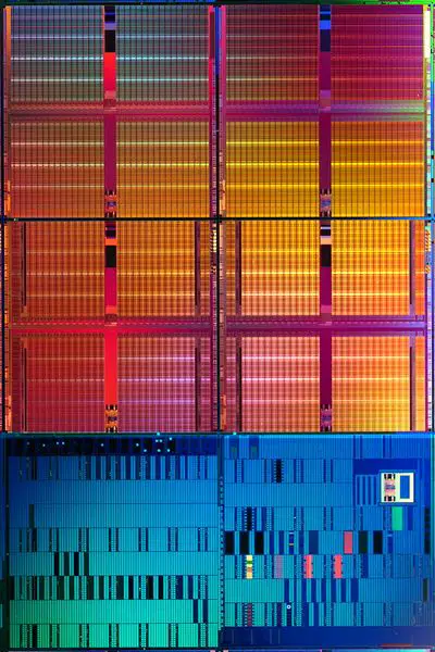
The 65 nanometer (65 nm) lithography process is a full node semiconductor manufacturing process following the 80 nm process stopgap.
- Commercial integrated circuit manufacturing using 65 nm process began in 2005.
This technology was superseded by the 55 nm process (HN) / 45 nm process (FN) in 2007.
Contents
Industry[edit]
Design Rules[edit]
| Intel 65 nm Design Rules | |||
|---|---|---|---|
| Layer | Pitch | Thick | Aspect Ratio |
| Isolation | 220 nm | 320 nm | - |
| Polysilicon | 220 nm | 90 nm | - |
| Contacted Gate |
220 nm | - | |
| Metal 1 | 210 nm | 170 nm | 1.6 |
| Metal 2 | 210 nm | 190 nm | 1.8 |
| Metal 3 | 220 nm | 200 nm | 1.8 |
| Metal 4 | 280 nm | 250 nm | 1.8 |
| Metal 5 | 330 nm | 300 nm | 1.8 |
| Metal 6 | 480 nm | 430 nm | 1.8 |
| Metal 7 | 720 nm | 650 nm | 1.8 |
| Metal 8 | 1.80 µm | 975 nm | 1.8 |
Specifications[edit]
| Fab / Manuf |
|---|
| Process Name |
| 1st Production |
| Wafer |
| Metal Layers |
| |
| Contacted Gate Pitch |
| Interconnect Pitch (M1P) |
| SRAM bit cell (HD) |
| SRAM bit cell (LP) |
| DRAM bit cell |
| Intel | IBM / Toshiba / Sony / AMD |
TI | IBM / Chartered / Infineon / Samsung |
TSMC | Fujitsu | ||||||
|---|---|---|---|---|---|---|---|---|---|---|---|
| P1264 | CS-200 / CS-201 / CS-250 | ||||||||||
| 2005 | 2005 | 2007 | 2005 | 2005 | 2006 | ||||||
| 300mm | |||||||||||
| 8 | 10 | 11 | 10 | 11 | |||||||
| Value | 90 nm Δ | Value | 90 nm Δ | Value | 90 nm Δ | Value | 90 nm Δ | Value | 90 nm Δ | Value | 90 nm Δ |
| 220 nm | 0.85x | 250 nm | ?x | ? nm | ?x | 200 nm | 0.82x | 160 nm | 0.67x | ? nm | ?x |
| 210 nm | 0.95x | ? nm | ?x | ? nm | ?x | 180 nm | 0.73 | 180 nm | 0.75x | ? nm | ?x |
| 0.570 µm² | 0.57x | 0.540 µm² | 0.49 µm² | 0.540 µm² | 0.55x | 0.499 µm² | 0.50x | ||||
| 0.680 µm² | 0.65 µm² | 0.65x | 0.49 µm² | 0.676 µm² | 0.54x | 0.525 µm² | 0.53x | ? µm² | ?x | ||
| 0.127 µm² | 0.67x | 0.189 µm² | 0.69x | ||||||||
65 nm Microprocessors[edit]
This list is incomplete; you can help by expanding it.
65 nm Microarchitectures[edit]
This list is incomplete; you can help by expanding it.
 Semiconductor lithography processes technology
