Semiconductor & Computer Engineering
| Edit Values | |
| Zen µarch | |
| General Info | |
| Arch Type | CPU |
| Designer | AMD |
| Manufacturer | GlobalFoundries |
| Introduction | March 2, 2017 |
| Process | 14 nm |
| Core Configs | 4, 6, 8, 12, 16, 24, 32 |
| Pipeline | |
| Type | Superscalar |
| OoOE | Yes |
| Speculative | Yes |
| Reg Renaming | Yes |
| Stages | 19 |
| Decode | 4-way |
| Instructions | |
| ISA | x86-64 |
| Extensions | MOVBE, MMX, SSE, SSE2, SSE3, SSSE3, SSE4.1, SSE4.2, POPCNT, AVX, AVX2, AES, PCLMUL, RDRND, F16C, BMI, BMI2, RDSEED, ADCX, PREFETCHW, CLFLUSHOPT, XSAVE, SHA, CLZERO |
| Cache | |
| L1I Cache | 64 KiB/core 4-way set associative |
| L1D Cache | 32 KiB/core 8-way set associative |
| L2 Cache | 512 KiB/core 8-way set associative |
| L3 Cache | 2 MiB/core 16-way set associative |
| Cores | |
| Core Names | Naples, Whitehaven, Summit Ridge, Raven Ridge, Snowy Owl, Great Horned Owl, Banded Kestrel |
| Succession | |
Zen (family 17h) is the microarchitecture developed by AMD as a successor to both Excavator and Puma. Zen is an entirely new design, built from the ground up for optimal balance of performance and power capable of covering the entire computing spectrum from fanless notebooks to high-performance desktop computers.
Zen was officially launched on March 2, 2017. Zen was replaced by Zen+ in 2018.
Contents
- 1 Etymology
- 2 Codenames
- 3 Process Technology
- 4 Brands
- 5 Release Dates
- 6 Compatibility
- 7 Compiler support
- 8 Architecture
- 9 All Zen Chips
- 10 Block Diagram
- 11 Core
- 12 Infinity Fabric
- 13 Clock domains
- 14 Security
- 15 Power
- 16 Features
- 17 Scalability
- 18 Memory Modes
- 19 Accelerated Processing Units
- 20 Die
- 21 Sockets/Platform
- 22 Designers
- 23 Bibliography
- 24 Documents
- 25 See also
Etymology[edit]
‘’Zen‘’ was picked by Michael Clark, AMD's senior fellow and lead architect.
- Zen was picked to represent the balance needed between the various competing aspects of a microprocessor - transistor allocation/die size, clock/frequency restriction, power limitations, and new instructions to implement.
- For performance desktop and mobile computing, Zen is branded as Athlon, Ryzen 3, Ryzen 5, Ryzen 7, Ryzen 9 and Ryzen Threadripper processors.
- For servers, Zen is branded as EPYC.
Codenames[edit]
| Core | C/T | Target |
|---|---|---|
| Naples | Up to 32/64 | High-end server multiprocessors |
| Whitehaven | Up to 16/32 | Enthusiasts market processors |
| Snowy Owl | Up to 16/32 | Embedded edge processors |
| Summit Ridge | Up to 8/16 | Mainstream to high-end desktops |
| Raven Ridge | Up to 4/8 | Mobile processors with Vega GPU |
| Great Horned Owl | Up to 4/8 | Embedded processors with Vega GPU |
| Dali | Up to 2/4 | Budget mobile processors with Vega GPU |
| Banded Kestrel | Up to 2/4 | Low-power/Cost-sensitive embedded processors with Vega GPU |
Process Technology[edit]
- See also: 14 nm process
Zen is manufactured on Global Foundries' 14 nm process Low Power Plus (14LPP). AMD's previous microarchitectures were based on 32 and 28 nanometer processes. The jump to 14 nm was part of AMD's attempt to remain competitive against Intel (both Skylake and Kaby Lake are also manufactured on 14 nm). The move to 14 nm will bring along related benefits of a smaller node such as reduced heat, reduced power consumption, and higher density for identical designs.
Comparison[edit]
| Core | Zen | Zen+ | Zen 2 | Zen 3 | Zen 3+ | Zen 4 | Zen 4c | Zen 5 | Zen 5c | Zen 6 | Zen 6c | |
|---|---|---|---|---|---|---|---|---|---|---|---|---|
| Codename | Core | Valhalla | Cerberus | Persephone | Dionysus | Nirvana | Prometheus | Morpheus | Monarch | |||
| CCD | Aspen Highlands |
Brecken Ridge |
Durango | Vindhya | Eldora | |||||||
| Cores (threads) |
CCD | 8 (16) | 8 (16) | 8 (16) | 16 (32) | 8 (16) | 16 (32) | |||||
| CCX | 4 (8) | 8 (16) | 8 (16) | 8 (16) | 8 (16) | |||||||
| L3 cache | CCD | 32 MB | 32 MB | 32 MB | 32 MB | 32 MB | 32 MB | |||||
| CCX | 16 MB | 32 MB | 32 MB | 16 MB | 32 MB | |||||||
| Die size | CCD area | 44 mm2 | 74 mm2 | 80.7 mm2 | 66.3 mm2 | 72.7 mm2 | 70.6 mm2 | |||||
| Core area (Fab node) |
7 mm2 (14 nm) |
(12 nm) | 2.83 mm2 (7 nm) |
3.24 mm2 (7 nm) |
(7 nm) | 3.84 mm2 (5 nm) |
2.48 mm2 (5 nm) |
(4 nm) | (3 nm) | (2 nm) | (2 nm) | |
Brands[edit]
| AMD Zen-based processor brands | ||||||||||
|---|---|---|---|---|---|---|---|---|---|---|
| Logo | Family | General Description | Differentiating Features | |||||||
| Cores | Unlocked | AVX2 | SMT | XFR | IGP | ECC | MP | |||
| Mainstream | ||||||||||
| |
Ryzen 3 | Entry level Performance | Quad | ✔ | ✔ | ✘ | ✔ | ✔/✘ | ✔ | ✘ |
| |
Ryzen 5 | Mid-range Performance | Quad | ✔ | ✔ | ✔ | ✔ | ✔/✘ | ✔ | ✘ |
| Hexa | ✔ | ✔ | ✔ | ✔ | ✘ | ✔ | ✘ | |||
| |
Ryzen 7 | High-end Performance | Octa | ✔ | ✔ | ✔ | ✔ | ✘ | ✔ | ✘ |
| |
Ryzen 9 | High-end Performance | 12-16 | ✔ | ✔ | ✔ | ✔ | ✘ | ✔ | ✘ |
| Enthusiasts / Workstations | ||||||||||
| |
Ryzen Threadripper | Enthusiasts | 8-16 | ✔ | ✔ | ✔ | ✔ | ✘ | ✔ | ✘ |
| Servers | ||||||||||
| |
EPYC | High-performance Server Processor | 8-32 | ✘ | ✔ | ✔ | ✘ | ✔ | ✔ | |
| Embedded / Edge | ||||||||||
| |
EPYC Embedded | Embedded / Edge Server Processor | 8-16 | ✘ | ✔ | ✔/✘ | ✘ | ✔ | ✘ | |
| |
Ryzen Embedded | Embedded APUs | 4 | ✔ | ✔/✘ | ✔ | ✔ | ✘ | ||
- Note: While a model has an unlocked multiplier, not all chipsets support overclocking. (see §Sockets)
- Note: 'X' models will enjoy "Full XFR" providing an additional +100 MHz (200 for 1500X and Threadripper line)
when sufficient thermo/electric requirements are met. Non-X models are limited to just +50 MHz.
Identification[edit]
| Identification | |||||||||||||||||||||||||||||||
| Ryzen | 7 | 1 | 7 | 00 | X | ||||||||||||||||||||||||||
| Ryzen | 5 | 3 | 5 | 50 | H | ||||||||||||||||||||||||||
Power Segment
| |||||||||||||||||||||||||||||||
| Model Number Speed bump and/or differentiator for high core count chips (8 cores+). | |||||||||||||||||||||||||||||||
Performance Level
| |||||||||||||||||||||||||||||||
Generation
| |||||||||||||||||||||||||||||||
Market segment
| |||||||||||||||||||||||||||||||
Brand Name
| |||||||||||||||||||||||||||||||
Release Dates[edit]

The first set of processors, as part of the Ryzen 7 family were introduced at an AMD event on February 22, 2017 before the Game Developer Conference (GDC). However initial models don't get shipped until March 2. Ryzen 5 hexa-core and quad-core variants were released on April 11, 2017. Server processors are set to be released in by the end of Q2, 2017. In October 2017, AMD launched mobile Zen-based processors featuring Vega GPUs.

Compatibility[edit]
Linux added initial support for Zen starting with Linux Kernel 4.10. Microsoft will only support Windows 10 for Zen.
| Vendor | OS | Version | Notes |
|---|---|---|---|
| Microsoft | Windows | Windows 7 | No Support |
| Windows 8 | No Support | ||
| Windows 10 | Support | ||
| Linux | Linux | Kernel 4.10 | Initial Support |
| Kernel 4.15 | Full Support |
Compiler support[edit]
With the release of Ryzen, AMD introduced their own compiler: AMD Optimizing C/C++ Compiler (AOCC).
AOCC is an LLVM port especially modified to generate optimized x86 code for the Zen microarchitecture.
| Compiler | Arch-Specific | Arch-Favorable |
|---|---|---|
| AOCC | -march=znver1 |
-mtune=znver1
|
| GCC | -march=znver1 |
-mtune=znver1
|
| LLVM | -march=znver1 |
-mtune=znver1
|
| Visual Studio | /arch:AVX2 |
? |
CPUID[edit]
- See also: AMD CPUID
| Core | Extended Family |
Family | Extended Model |
Model |
|---|---|---|---|---|
| Naples, Whitehaven, Summit Ridge | 0x8 | 0xF | 0x0 | 0x1 |
| Family 23 Model 1 | ||||
| Raven Ridge | 0x8 | 0xF | 0x1 | 0x1 |
| Family 23 Model 17 | ||||
Architecture[edit]
AMD Zen is an entirely new design from the ground up which introduces considerable amount of improvements and design changes over Excavator.
Mainstream Zen-based microprocessors utilize AMD's Socket AM4 unified platform along with the Promontory chipset.
Key changes from Excavator[edit]
|
New instructions[edit] |
While not new, Zen also supports AVX, AVX2, FMA3, BMI1, BMI2, AES, RdRand, SMEP. Note that with Zen, AMD dropped support for XOP, TBM and LWP.
Note: WikiChip's testing shows FMA4 still works despite not being officially supported and not even reported by CPUID.
This has also been confirmed by Agner here. Those tests were not exhaustive. Never use them in production.
Memory Hierarchy[edit]
|
Zen TLB consists of dedicated level one TLB for instruction cache and another one for data cache.
|
All Zen Chips[edit]
| List of all Zen-based Processors | |||||||||||||||||||||||||
|---|---|---|---|---|---|---|---|---|---|---|---|---|---|---|---|---|---|---|---|---|---|---|---|---|---|
| Processor | Features | ||||||||||||||||||||||||
| Model | Family | Core | C | T | Freq | Turbo | TDP | L3$ | L2$ | L1$ | Max Mem | Process | Launched | Price | SMT | AMD-V | XFR | SEV | SME | TSME | |||||
| Uniprocessors | |||||||||||||||||||||||||
| 200GE | Athlon | Raven Ridge | 2 | 4 | 3.2 GHz 3,200 MHz 3,200,000 kHz | 35 W 35,000 mW 0.0469 hp 0.035 kW | 4 MiB 4,096 KiB 4,194,304 B 0.00391 GiB | 1 MiB 1,024 KiB 1,048,576 B 9.765625e-4 GiB | 192 KiB 196,608 B 0.188 MiB | 64 GiB 65,536 MiB 67,108,864 KiB 68,719,476,736 B 0.0625 TiB | 14 nm 0.014 μm 1.4e-5 mm | 6 September 2018 | $ 55.00 € 49.50 £ 44.55 ¥ 5,683.15 | ✔ | ✔ | ✘ | ✘ | ✘ | ✘ | ||||||
| 220GE | Athlon | Raven Ridge | 2 | 4 | 3.4 GHz 3,400 MHz 3,400,000 kHz | 35 W 35,000 mW 0.0469 hp 0.035 kW | 4 MiB 4,096 KiB 4,194,304 B 0.00391 GiB | 1 MiB 1,024 KiB 1,048,576 B 9.765625e-4 GiB | 192 KiB 196,608 B 0.188 MiB | 64 GiB 65,536 MiB 67,108,864 KiB 68,719,476,736 B 0.0625 TiB | 14 nm 0.014 μm 1.4e-5 mm | 21 December 2018 | $ 65.00 € 58.50 £ 52.65 ¥ 6,716.45 | ✔ | ✔ | ✘ | ✘ | ✘ | ✘ | ||||||
| 240GE | Athlon | Raven Ridge | 2 | 4 | 3.5 GHz 3,500 MHz 3,500,000 kHz | 35 W 35,000 mW 0.0469 hp 0.035 kW | 4 MiB 4,096 KiB 4,194,304 B 0.00391 GiB | 1 MiB 1,024 KiB 1,048,576 B 9.765625e-4 GiB | 192 KiB 196,608 B 0.188 MiB | 64 GiB 65,536 MiB 67,108,864 KiB 68,719,476,736 B 0.0625 TiB | 14 nm 0.014 μm 1.4e-5 mm | 21 December 2018 | $ 75.00 € 67.50 £ 60.75 ¥ 7,749.75 | ✔ | ✔ | ✘ | ✘ | ✘ | ✘ | ||||||
| 3000G | Athlon | Dali, Raven Ridge | 2 | 4 | 3.5 GHz 3,500 MHz 3,500,000 kHz | 35 W 35,000 mW 0.0469 hp 0.035 kW | 4 MiB 4,096 KiB 4,194,304 B 0.00391 GiB | 1 MiB 1,024 KiB 1,048,576 B 9.765625e-4 GiB | 192 KiB 196,608 B 0.188 MiB | 64 GiB 65,536 MiB 67,108,864 KiB 68,719,476,736 B 0.0625 TiB | 14 nm 0.014 μm 1.4e-5 mm | 20 November 2019 | $ 49.00 € 44.10 £ 39.69 ¥ 5,063.17 | ✔ | ✔ | ✔ | ✔ | ✔ | ✘ | ||||||
| 300U | Athlon | Raven Ridge | 2 | 4 | 2.4 GHz 2,400 MHz 2,400,000 kHz | 15 W 15,000 mW 0.0201 hp 0.015 kW | 4 MiB 4,096 KiB 4,194,304 B 0.00391 GiB | 1 MiB 1,024 KiB 1,048,576 B 9.765625e-4 GiB | 192 KiB 196,608 B 0.188 MiB | 64 GiB 65,536 MiB 67,108,864 KiB 68,719,476,736 B 0.0625 TiB | 14 nm 0.014 μm 1.4e-5 mm | 6 January 2019 | ✔ | ✔ | ✘ | ✘ | ✘ | ✘ | |||||||
| 3150U | Athlon Gold | Dali | 2 | 4 | 2.4 GHz 2,400 MHz 2,400,000 kHz | 15 W 15,000 mW 0.0201 hp 0.015 kW | 4 MiB 4,096 KiB 4,194,304 B 0.00391 GiB | 1 MiB 1,024 KiB 1,048,576 B 9.765625e-4 GiB | 192 KiB 196,608 B 0.188 MiB | 32 GiB 32,768 MiB 33,554,432 KiB 34,359,738,368 B 0.0313 TiB | 14 nm 0.014 μm 1.4e-5 mm | 6 January 2020 | ✔ | ✔ | ✘ | ✘ | ✘ | ✘ | |||||||
| PRO 200GE | Athlon | Raven Ridge | 2 | 4 | 3.2 GHz 3,200 MHz 3,200,000 kHz | 35 W 35,000 mW 0.0469 hp 0.035 kW | 4 MiB 4,096 KiB 4,194,304 B 0.00391 GiB | 1 MiB 1,024 KiB 1,048,576 B 9.765625e-4 GiB | 192 KiB 196,608 B 0.188 MiB | 64 GiB 65,536 MiB 67,108,864 KiB 68,719,476,736 B 0.0625 TiB | 14 nm 0.014 μm 1.4e-5 mm | 6 September 2018 | ✔ | ✔ | ✘ | ✘ | ✘ | ✔ | |||||||
| 3050U | Athlon Silver | Dali | 2 | 2 | 2.3 GHz 2,300 MHz 2,300,000 kHz | 15 W 15,000 mW 0.0201 hp 0.015 kW | 4 MiB 4,096 KiB 4,194,304 B 0.00391 GiB | 1 MiB 1,024 KiB 1,048,576 B 9.765625e-4 GiB | 192 KiB 196,608 B 0.188 MiB | 32 GiB 32,768 MiB 33,554,432 KiB 34,359,738,368 B 0.0313 TiB | 14 nm 0.014 μm 1.4e-5 mm | 6 January 2020 | ✔ | ✔ | ✘ | ✘ | ✘ | ✘ | |||||||
| 7351P | EPYC | Naples | 16 | 32 | 2.4 GHz 2,400 MHz 2,400,000 kHz | 2.9 GHz 2,900 MHz 2,900,000 kHz | 155 W 155,000 mW , 170 W0.208 hp 0.155 kW 170,000 mW 0.228 hp 0.17 kW | 64 MiB 65,536 KiB 67,108,864 B 0.0625 GiB | 8 MiB 8,192 KiB 8,388,608 B 0.00781 GiB | 1,536 KiB 1,572,864 B 1.5 MiB | 2,048 GiB 2,097,152 MiB 2,147,483,648 KiB 2,199,023,255,552 B 2 TiB | 14 nm 0.014 μm 1.4e-5 mm | 20 June 2017 | $ 750.00 € 675.00 £ 607.50 ¥ 77,497.50 | ✔ | ✔ | ✘ | ✔ | ✔ | ✔ | |||||
| 7401P | EPYC | Naples | 24 | 48 | 2 GHz 2,000 MHz 2,000,000 kHz | 3 GHz 3,000 MHz 3,000,000 kHz | 155 W 155,000 mW , 170 W0.208 hp 0.155 kW 170,000 mW 0.228 hp 0.17 kW | 64 MiB 65,536 KiB 67,108,864 B 0.0625 GiB | 12 MiB 12,288 KiB 12,582,912 B 0.0117 GiB | 2,304 KiB 2,359,296 B 2.25 MiB | 2,048 GiB 2,097,152 MiB 2,147,483,648 KiB 2,199,023,255,552 B 2 TiB | 14 nm 0.014 μm 1.4e-5 mm | 20 June 2017 | $ 1,075.00 € 967.50 £ 870.75 ¥ 111,079.75 | ✔ | ✔ | ✘ | ✔ | ✔ | ✔ | |||||
| 7551P | EPYC | Naples | 32 | 64 | 2 GHz 2,000 MHz 2,000,000 kHz | 3 GHz 3,000 MHz 3,000,000 kHz | 180 W 180,000 mW 0.241 hp 0.18 kW | 64 MiB 65,536 KiB 67,108,864 B 0.0625 GiB | 16 MiB 16,384 KiB 16,777,216 B 0.0156 GiB | 3,072 KiB 3,145,728 B 3 MiB | 2,048 GiB 2,097,152 MiB 2,147,483,648 KiB 2,199,023,255,552 B 2 TiB | 14 nm 0.014 μm 1.4e-5 mm | 20 June 2017 | $ 2,100.00 € 1,890.00 £ 1,701.00 ¥ 216,993.00 | ✔ | ✔ | ✘ | ✔ | ✔ | ✔ | |||||
| 3101 | EPYC Embedded | Snowy Owl | 4 | 4 | 2.1 GHz 2,100 MHz 2,100,000 kHz | 2.9 GHz 2,900 MHz 2,900,000 kHz | 35 W 35,000 mW 0.0469 hp 0.035 kW | 8 MiB 8,192 KiB 8,388,608 B 0.00781 GiB | 2 MiB 2,048 KiB 2,097,152 B 0.00195 GiB | 384 KiB 393,216 B 0.375 MiB | 512 GiB 524,288 MiB 536,870,912 KiB 549,755,813,888 B 0.5 TiB | 14 nm 0.014 μm 1.4e-5 mm | 21 February 2018 | ✘ | ✔ | ✘ | ✔ | ✔ | ✔ | ||||||
| 3151 | EPYC Embedded | Snowy Owl | 4 | 8 | 2.7 GHz 2,700 MHz 2,700,000 kHz | 2.9 GHz 2,900 MHz 2,900,000 kHz | 45 W 45,000 mW 0.0603 hp 0.045 kW | 16 MiB 16,384 KiB 16,777,216 B 0.0156 GiB | 2 MiB 2,048 KiB 2,097,152 B 0.00195 GiB | 384 KiB 393,216 B 0.375 MiB | 512 GiB 524,288 MiB 536,870,912 KiB 549,755,813,888 B 0.5 TiB | 14 nm 0.014 μm 1.4e-5 mm | 21 February 2018 | ✔ | ✔ | ✘ | ✔ | ✔ | ✔ | ||||||
| 3201 | EPYC Embedded | Snowy Owl | 8 | 8 | 1.5 GHz 1,500 MHz 1,500,000 kHz | 3.1 GHz 3,100 MHz 3,100,000 kHz | 30 W 30,000 mW 0.0402 hp 0.03 kW | 16 MiB 16,384 KiB 16,777,216 B 0.0156 GiB | 4 MiB 4,096 KiB 4,194,304 B 0.00391 GiB | 768 KiB 786,432 B 0.75 MiB | 512 GiB 524,288 MiB 536,870,912 KiB 549,755,813,888 B 0.5 TiB | 14 nm 0.014 μm 1.4e-5 mm | 21 February 2018 | ✘ | ✔ | ✘ | ✔ | ✔ | ✔ | ||||||
| 3251 | EPYC Embedded | Snowy Owl | 8 | 16 | 2.5 GHz 2,500 MHz 2,500,000 kHz | 3.1 GHz 3,100 MHz 3,100,000 kHz | 55 W 55,000 mW 0.0738 hp 0.055 kW | 16 MiB 16,384 KiB 16,777,216 B 0.0156 GiB | 4 MiB 4,096 KiB 4,194,304 B 0.00391 GiB | 768 KiB 786,432 B 0.75 MiB | 512 GiB 524,288 MiB 536,870,912 KiB 549,755,813,888 B 0.5 TiB | 14 nm 0.014 μm 1.4e-5 mm | 21 February 2018 | $ 315.00 € 283.50 £ 255.15 ¥ 32,548.95 | ✔ | ✔ | ✘ | ✔ | ✔ | ✔ | |||||
| 3255 | EPYC Embedded | Snowy Owl | 8 | 16 | 2.5 GHz 2,500 MHz 2,500,000 kHz | 3.1 GHz 3,100 MHz 3,100,000 kHz | 55 W 55,000 mW 0.0738 hp 0.055 kW | 16 MiB 16,384 KiB 16,777,216 B 0.0156 GiB | 4 MiB 4,096 KiB 4,194,304 B 0.00391 GiB | 768 KiB 786,432 B 0.75 MiB | 512 GiB 524,288 MiB 536,870,912 KiB 549,755,813,888 B 0.5 TiB | 14 nm 0.014 μm 1.4e-5 mm | ✔ | ✔ | ✘ | ✔ | ✔ | ✔ | |||||||
| 3301 | EPYC Embedded | Snowy Owl | 12 | 12 | 2 GHz 2,000 MHz 2,000,000 kHz | 3 GHz 3,000 MHz 3,000,000 kHz | 65 W 65,000 mW 0.0872 hp 0.065 kW | 32 MiB 32,768 KiB 33,554,432 B 0.0313 GiB | 6 MiB 6,144 KiB 6,291,456 B 0.00586 GiB | 1,152 KiB 1,179,648 B 1.125 MiB | 1,024 GiB 1,048,576 MiB 1,073,741,824 KiB 1,099,511,627,776 B 1 TiB | 14 nm 0.014 μm 1.4e-5 mm | 21 February 2018 | $ 450.00 € 405.00 £ 364.50 ¥ 46,498.50 | ✘ | ✔ | ✘ | ✔ | ✔ | ✔ | |||||
| 3351 | EPYC Embedded | Snowy Owl | 12 | 24 | 1.9 GHz 1,900 MHz 1,900,000 kHz | 3 GHz 3,000 MHz 3,000,000 kHz | 80 W 80,000 mW 0.107 hp 0.08 kW | 32 MiB 32,768 KiB 33,554,432 B 0.0313 GiB | 6 MiB 6,144 KiB 6,291,456 B 0.00586 GiB | 1,152 KiB 1,179,648 B 1.125 MiB | 1,024 GiB 1,048,576 MiB 1,073,741,824 KiB 1,099,511,627,776 B 1 TiB | 14 nm 0.014 μm 1.4e-5 mm | 21 February 2018 | ✔ | ✔ | ✘ | ✔ | ✔ | ✔ | ||||||
| 3401 | EPYC Embedded | Snowy Owl | 16 | 16 | 1.85 GHz 1,850 MHz 1,850,000 kHz | 3 GHz 3,000 MHz 3,000,000 kHz | 85 W 85,000 mW 0.114 hp 0.085 kW | 32 MiB 32,768 KiB 33,554,432 B 0.0313 GiB | 8 MiB 8,192 KiB 8,388,608 B 0.00781 GiB | 1,536 KiB 1,572,864 B 1.5 MiB | 1,024 GiB 1,048,576 MiB 1,073,741,824 KiB 1,099,511,627,776 B 1 TiB | 14 nm 0.014 μm 1.4e-5 mm | 21 February 2018 | ✘ | ✔ | ✘ | ✔ | ✔ | ✔ | ||||||
| 3451 | EPYC Embedded | Snowy Owl | 16 | 32 | 2.15 GHz 2,150 MHz 2,150,000 kHz | 3 GHz 3,000 MHz 3,000,000 kHz | 100 W 100,000 mW 0.134 hp 0.1 kW | 32 MiB 32,768 KiB 33,554,432 B 0.0313 GiB | 8 MiB 8,192 KiB 8,388,608 B 0.00781 GiB | 1,536 KiB 1,572,864 B 1.5 MiB | 1,024 GiB 1,048,576 MiB 1,073,741,824 KiB 1,099,511,627,776 B 1 TiB | 14 nm 0.014 μm 1.4e-5 mm | 21 February 2018 | $ 880.00 € 792.00 £ 712.80 ¥ 90,930.40 | ✔ | ✔ | ✘ | ✔ | ✔ | ✔ | |||||
| FireFlight | 4 | 8 | 3 GHz 3,000 MHz 3,000,000 kHz | 4 MiB 4,096 KiB 4,194,304 B 0.00391 GiB | 2 MiB 2,048 KiB 2,097,152 B 0.00195 GiB | 384 KiB 393,216 B 0.375 MiB | 8 GiB 8,192 MiB 8,388,608 KiB 8,589,934,592 B 0.00781 TiB | 3 August 2018 | ✔ | ✔ | ✔ | ✘ | ✘ | ✘ | |||||||||||
| 1200 | Ryzen 3 | Summit Ridge | 4 | 4 | 3.1 GHz 3,100 MHz 3,100,000 kHz | 3.4 GHz 3,400 MHz 3,400,000 kHz | 65 W 65,000 mW 0.0872 hp 0.065 kW | 8 MiB 8,192 KiB 8,388,608 B 0.00781 GiB | 2 MiB 2,048 KiB 2,097,152 B 0.00195 GiB | 384 KiB 393,216 B 0.375 MiB | 64 GiB 65,536 MiB 67,108,864 KiB 68,719,476,736 B 0.0625 TiB | 14 nm 0.014 μm 1.4e-5 mm | 27 July 2017 | $ 109.00 € 98.10 £ 88.29 ¥ 11,262.97 | ✘ | ✔ | ✘ | ✘ | ✘ | ✘ | |||||
| 1300X | Ryzen 3 | Summit Ridge | 4 | 4 | 3.5 GHz 3,500 MHz 3,500,000 kHz | 3.7 GHz 3,700 MHz 3,700,000 kHz | 65 W 65,000 mW 0.0872 hp 0.065 kW | 8 MiB 8,192 KiB 8,388,608 B 0.00781 GiB | 2 MiB 2,048 KiB 2,097,152 B 0.00195 GiB | 384 KiB 393,216 B 0.375 MiB | 64 GiB 65,536 MiB 67,108,864 KiB 68,719,476,736 B 0.0625 TiB | 14 nm 0.014 μm 1.4e-5 mm | 27 July 2017 | $ 129.00 € 116.10 £ 104.49 ¥ 13,329.57 | ✔ | ✔ | ✔ | ✘ | ✘ | ✘ | |||||
| 2200G | Ryzen 3 | Raven Ridge | 4 | 4 | 3.5 GHz 3,500 MHz 3,500,000 kHz | 3.7 GHz 3,700 MHz 3,700,000 kHz | 65 W 65,000 mW 0.0872 hp 0.065 kW | 4 MiB 4,096 KiB 4,194,304 B 0.00391 GiB | 2 MiB 2,048 KiB 2,097,152 B 0.00195 GiB | 384 KiB 393,216 B 0.375 MiB | 64 GiB 65,536 MiB 67,108,864 KiB 68,719,476,736 B 0.0625 TiB | 14 nm 0.014 μm 1.4e-5 mm | 12 February 2018 | $ 99.00 € 89.10 £ 80.19 ¥ 10,229.67 | ✘ | ✔ | ✔ | ✘ | ✘ | ✘ | |||||
| 2200GE | Ryzen 3 | Raven Ridge | 4 | 4 | 3.2 GHz 3,200 MHz 3,200,000 kHz | 3.6 GHz 3,600 MHz 3,600,000 kHz | 35 W 35,000 mW 0.0469 hp 0.035 kW | 4 MiB 4,096 KiB 4,194,304 B 0.00391 GiB | 2 MiB 2,048 KiB 2,097,152 B 0.00195 GiB | 384 KiB 393,216 B 0.375 MiB | 64 GiB 65,536 MiB 67,108,864 KiB 68,719,476,736 B 0.0625 TiB | 14 nm 0.014 μm 1.4e-5 mm | 19 April 2018 | ✘ | ✔ | ✔ | ✘ | ✘ | ✘ | ||||||
| 2200U | Ryzen 3 | Raven Ridge | 2 | 4 | 2.5 GHz 2,500 MHz 2,500,000 kHz | 3.4 GHz 3,400 MHz 3,400,000 kHz | 15 W 15,000 mW 0.0201 hp 0.015 kW | 4 MiB 4,096 KiB 4,194,304 B 0.00391 GiB | 1 MiB 1,024 KiB 1,048,576 B 9.765625e-4 GiB | 192 KiB 196,608 B 0.188 MiB | 32 GiB 32,768 MiB 33,554,432 KiB 34,359,738,368 B 0.0313 TiB | 14 nm 0.014 μm 1.4e-5 mm | 8 January 2018 | ✔ | ✔ | ✘ | ✘ | ✘ | ✘ | ||||||
| 2300U | Ryzen 3 | Raven Ridge | 4 | 4 | 2 GHz 2,000 MHz 2,000,000 kHz | 3.4 GHz 3,400 MHz 3,400,000 kHz | 15 W 15,000 mW 0.0201 hp 0.015 kW | 4 MiB 4,096 KiB 4,194,304 B 0.00391 GiB | 2 MiB 2,048 KiB 2,097,152 B 0.00195 GiB | 384 KiB 393,216 B 0.375 MiB | 32 GiB 32,768 MiB 33,554,432 KiB 34,359,738,368 B 0.0313 TiB | 14 nm 0.014 μm 1.4e-5 mm | 8 January 2018 | ✘ | ✔ | ✘ | ✘ | ✘ | ✘ | ||||||
| 3250U | Ryzen 3 | Dali | 2 | 4 | 2.6 GHz 2,600 MHz 2,600,000 kHz | 15 W 15,000 mW 0.0201 hp 0.015 kW | 4 MiB 4,096 KiB 4,194,304 B 0.00391 GiB | 1 MiB 1,024 KiB 1,048,576 B 9.765625e-4 GiB | 192 KiB 196,608 B 0.188 MiB | 32 GiB 32,768 MiB 33,554,432 KiB 34,359,738,368 B 0.0313 TiB | 14 nm 0.014 μm 1.4e-5 mm | 6 January 2020 | ✔ | ✔ | ✘ | ✘ | ✘ | ✘ | |||||||
| PRO 1200 | Ryzen 3 | Summit Ridge | 4 | 4 | 3.1 GHz 3,100 MHz 3,100,000 kHz | 3.4 GHz 3,400 MHz 3,400,000 kHz | 65 W 65,000 mW 0.0872 hp 0.065 kW | 8 MiB 8,192 KiB 8,388,608 B 0.00781 GiB | 2 MiB 2,048 KiB 2,097,152 B 0.00195 GiB | 384 KiB 393,216 B 0.375 MiB | 64 GiB 65,536 MiB 67,108,864 KiB 68,719,476,736 B 0.0625 TiB | 14 nm 0.014 μm 1.4e-5 mm | ✔ | ✔ | ✘ | ✘ | ✘ | ✔ | |||||||
| PRO 1300 | Ryzen 3 | Summit Ridge | 4 | 4 | 3.5 GHz 3,500 MHz 3,500,000 kHz | 3.7 GHz 3,700 MHz 3,700,000 kHz | 65 W 65,000 mW 0.0872 hp 0.065 kW | 8 MiB 8,192 KiB 8,388,608 B 0.00781 GiB | 2 MiB 2,048 KiB 2,097,152 B 0.00195 GiB | 384 KiB 393,216 B 0.375 MiB | 64 GiB 65,536 MiB 67,108,864 KiB 68,719,476,736 B 0.0625 TiB | 14 nm 0.014 μm 1.4e-5 mm | ✔ | ✔ | ✘ | ✘ | ✘ | ✔ | |||||||
| PRO 2200G | Ryzen 3 | Raven Ridge | 4 | 4 | 3.5 GHz 3,500 MHz 3,500,000 kHz | 3.7 GHz 3,700 MHz 3,700,000 kHz | 65 W 65,000 mW 0.0872 hp 0.065 kW | 4 MiB 4,096 KiB 4,194,304 B 0.00391 GiB | 2 MiB 2,048 KiB 2,097,152 B 0.00195 GiB | 384 KiB 393,216 B 0.375 MiB | 64 GiB 65,536 MiB 67,108,864 KiB 68,719,476,736 B 0.0625 TiB | 14 nm 0.014 μm 1.4e-5 mm | 10 May 2018 | ✘ | ✔ | ✘ | ✘ | ✘ | ✔ | ||||||
| PRO 2200GE | Ryzen 3 | Raven Ridge | 4 | 4 | 3.2 GHz 3,200 MHz 3,200,000 kHz | 3.6 GHz 3,600 MHz 3,600,000 kHz | 35 W 35,000 mW 0.0469 hp 0.035 kW | 4 MiB 4,096 KiB 4,194,304 B 0.00391 GiB | 2 MiB 2,048 KiB 2,097,152 B 0.00195 GiB | 384 KiB 393,216 B 0.375 MiB | 64 GiB 65,536 MiB 67,108,864 KiB 68,719,476,736 B 0.0625 TiB | 14 nm 0.014 μm 1.4e-5 mm | 10 May 2018 | ✘ | ✔ | ✔ | ✘ | ✘ | ✔ | ||||||
| PRO 2300U | Ryzen 3 | Raven Ridge | 4 | 4 | 2 GHz 2,000 MHz 2,000,000 kHz | 3.4 GHz 3,400 MHz 3,400,000 kHz | 15 W 15,000 mW 0.0201 hp 0.015 kW | 4 MiB 4,096 KiB 4,194,304 B 0.00391 GiB | 2 MiB 2,048 KiB 2,097,152 B 0.00195 GiB | 384 KiB 393,216 B 0.375 MiB | 32 GiB 32,768 MiB 33,554,432 KiB 34,359,738,368 B 0.0313 TiB | 14 nm 0.014 μm 1.4e-5 mm | 8 January 2018 | ✘ | ✔ | ✘ | ✘ | ✘ | ✔ | ||||||
| 1400 | Ryzen 5 | Summit Ridge | 4 | 8 | 3.2 GHz 3,200 MHz 3,200,000 kHz | 3.4 GHz 3,400 MHz 3,400,000 kHz | 65 W 65,000 mW 0.0872 hp 0.065 kW | 8 MiB 8,192 KiB 8,388,608 B 0.00781 GiB | 2 MiB 2,048 KiB 2,097,152 B 0.00195 GiB | 384 KiB 393,216 B 0.375 MiB | 64 GiB 65,536 MiB 67,108,864 KiB 68,719,476,736 B 0.0625 TiB | 14 nm 0.014 μm 1.4e-5 mm | 11 April 2017 | $ 169.00 € 152.10 £ 136.89 ¥ 17,462.77 | ✔ | ✔ | ✘ | ✘ | ✘ | ✘ | |||||
| 1500X | Ryzen 5 | Summit Ridge | 4 | 8 | 3.5 GHz 3,500 MHz 3,500,000 kHz | 3.7 GHz 3,700 MHz 3,700,000 kHz | 65 W 65,000 mW 0.0872 hp 0.065 kW | 16 MiB 16,384 KiB 16,777,216 B 0.0156 GiB | 2 MiB 2,048 KiB 2,097,152 B 0.00195 GiB | 384 KiB 393,216 B 0.375 MiB | 64 GiB 65,536 MiB 67,108,864 KiB 68,719,476,736 B 0.0625 TiB | 14 nm 0.014 μm 1.4e-5 mm | 11 April 2017 | $ 189.00 € 170.10 £ 153.09 ¥ 19,529.37 | ✔ | ✔ | ✔ | ✘ | ✘ | ✘ | |||||
| 1600 | Ryzen 5 | Summit Ridge | 6 | 12 | 3.2 GHz 3,200 MHz 3,200,000 kHz | 3.6 GHz 3,600 MHz 3,600,000 kHz | 65 W 65,000 mW 0.0872 hp 0.065 kW | 16 MiB 16,384 KiB 16,777,216 B 0.0156 GiB | 3 MiB 3,072 KiB 3,145,728 B 0.00293 GiB | 576 KiB 589,824 B 0.563 MiB | 64 GiB 65,536 MiB 67,108,864 KiB 68,719,476,736 B 0.0625 TiB | 14 nm 0.014 μm 1.4e-5 mm | 11 April 2017 | $ 219.00 € 197.10 £ 177.39 ¥ 22,629.27 | ✔ | ✘ | ✘ | ✘ | ✘ | ✘ | |||||
| 1600X | Ryzen 5 | Summit Ridge | 6 | 12 | 3.6 GHz 3,600 MHz 3,600,000 kHz | 4 GHz 4,000 MHz 4,000,000 kHz | 95 W 95,000 mW 0.127 hp 0.095 kW | 16 MiB 16,384 KiB 16,777,216 B 0.0156 GiB | 3 MiB 3,072 KiB 3,145,728 B 0.00293 GiB | 576 KiB 589,824 B 0.563 MiB | 64 GiB 65,536 MiB 67,108,864 KiB 68,719,476,736 B 0.0625 TiB | 14 nm 0.014 μm 1.4e-5 mm | 11 April 2017 | $ 249.00 € 224.10 £ 201.69 ¥ 25,729.17 | ✔ | ✔ | ✔ | ✘ | ✘ | ✘ | |||||
| 2400G | Ryzen 5 | Raven Ridge | 4 | 8 | 3.6 GHz 3,600 MHz 3,600,000 kHz | 3.9 GHz 3,900 MHz 3,900,000 kHz | 65 W 65,000 mW 0.0872 hp 0.065 kW | 4 MiB 4,096 KiB 4,194,304 B 0.00391 GiB | 2 MiB 2,048 KiB 2,097,152 B 0.00195 GiB | 386 KiB 395,264 B 0.377 MiB | 64 GiB 65,536 MiB 67,108,864 KiB 68,719,476,736 B 0.0625 TiB | 14 nm 0.014 μm 1.4e-5 mm | 12 February 2018 | $ 169.00 € 152.10 £ 136.89 ¥ 17,462.77 | ✔ | ✔ | ✘ | ✘ | ✘ | ✘ | |||||
| 2400GE | Ryzen 5 | Raven Ridge | 4 | 8 | 3.2 GHz 3,200 MHz 3,200,000 kHz | 3.8 GHz 3,800 MHz 3,800,000 kHz | 35 W 35,000 mW 0.0469 hp 0.035 kW | 4 MiB 4,096 KiB 4,194,304 B 0.00391 GiB | 2 MiB 2,048 KiB 2,097,152 B 0.00195 GiB | 384 KiB 393,216 B 0.375 MiB | 64 GiB 65,536 MiB 67,108,864 KiB 68,719,476,736 B 0.0625 TiB | 14 nm 0.014 μm 1.4e-5 mm | 19 April 2018 | ✔ | ✔ | ✘ | ✘ | ✘ | ✘ | ||||||
| 2500U | Ryzen 5 | Raven Ridge | 4 | 8 | 2 GHz 2,000 MHz 2,000,000 kHz | 3.6 GHz 3,600 MHz 3,600,000 kHz | 15 W 15,000 mW 0.0201 hp 0.015 kW | 4 MiB 4,096 KiB 4,194,304 B 0.00391 GiB | 2 MiB 2,048 KiB 2,097,152 B 0.00195 GiB | 384 KiB 393,216 B 0.375 MiB | 32 GiB 32,768 MiB 33,554,432 KiB 34,359,738,368 B 0.0313 TiB | 14 nm 0.014 μm 1.4e-5 mm | 26 October 2017 | ✔ | ✔ | ✘ | ✘ | ✘ | ✘ | ||||||
| 2600H | Ryzen 5 | Raven Ridge | 4 | 8 | 3.2 GHz 3,200 MHz 3,200,000 kHz | 3.6 GHz 3,600 MHz 3,600,000 kHz | 45 W 45,000 mW 0.0603 hp 0.045 kW | 4 MiB 4,096 KiB 4,194,304 B 0.00391 GiB | 2 MiB 2,048 KiB 2,097,152 B 0.00195 GiB | 384 KiB 393,216 B 0.375 MiB | 32 GiB 32,768 MiB 33,554,432 KiB 34,359,738,368 B 0.0313 TiB | 14 nm 0.014 μm 1.4e-5 mm | 10 September 2018 | ✔ | ✔ | ✘ | ✘ | ✘ | ✘ | ||||||
| PRO 1500 | Ryzen 5 | Summit Ridge | 4 | 8 | 3.5 GHz 3,500 MHz 3,500,000 kHz | 3.7 GHz 3,700 MHz 3,700,000 kHz | 65 W 65,000 mW 0.0872 hp 0.065 kW | 16 MiB 16,384 KiB 16,777,216 B 0.0156 GiB | 2 MiB 2,048 KiB 2,097,152 B 0.00195 GiB | 384 KiB 393,216 B 0.375 MiB | 64 GiB 65,536 MiB 67,108,864 KiB 68,719,476,736 B 0.0625 TiB | 14 nm 0.014 μm 1.4e-5 mm | 29 June 2017 | ✔ | ✔ | ✘ | ✘ | ✘ | ✔ | ||||||
| PRO 1600 | Ryzen 5 | Summit Ridge | 6 | 12 | 3.2 GHz 3,200 MHz 3,200,000 kHz | 3.6 GHz 3,600 MHz 3,600,000 kHz | 65 W 65,000 mW 0.0872 hp 0.065 kW | 16 MiB 16,384 KiB 16,777,216 B 0.0156 GiB | 3 MiB 3,072 KiB 3,145,728 B 0.00293 GiB | 576 KiB 589,824 B 0.563 MiB | 64 GiB 65,536 MiB 67,108,864 KiB 68,719,476,736 B 0.0625 TiB | 14 nm 0.014 μm 1.4e-5 mm | ✔ | ✔ | ✘ | ✘ | ✘ | ✔ | |||||||
| PRO 2400G | Ryzen 5 | Raven Ridge | 4 | 8 | 3.6 GHz 3,600 MHz 3,600,000 kHz | 3.9 GHz 3,900 MHz 3,900,000 kHz | 65 W 65,000 mW 0.0872 hp 0.065 kW | 4 MiB 4,096 KiB 4,194,304 B 0.00391 GiB | 2 MiB 2,048 KiB 2,097,152 B 0.00195 GiB | 384 KiB 393,216 B 0.375 MiB | 64 GiB 65,536 MiB 67,108,864 KiB 68,719,476,736 B 0.0625 TiB | 14 nm 0.014 μm 1.4e-5 mm | 10 May 2018 | $ 169.00 € 152.10 £ 136.89 ¥ 17,462.77 | ✔ | ✔ | ✘ | ✘ | ✘ | ✔ | |||||
| PRO 2400GE | Ryzen 5 | Raven Ridge | 4 | 8 | 3.2 GHz 3,200 MHz 3,200,000 kHz | 3.8 GHz 3,800 MHz 3,800,000 kHz | 35 W 35,000 mW 0.0469 hp 0.035 kW | 4 MiB 4,096 KiB 4,194,304 B 0.00391 GiB | 2 MiB 2,048 KiB 2,097,152 B 0.00195 GiB | 384 KiB 393,216 B 0.375 MiB | 64 GiB 65,536 MiB 67,108,864 KiB 68,719,476,736 B 0.0625 TiB | 14 nm 0.014 μm 1.4e-5 mm | 10 May 2018 | ✔ | ✔ | ✘ | ✘ | ✘ | ✔ | ||||||
| PRO 2500U | Ryzen 5 | Raven Ridge | 4 | 8 | 2 GHz 2,000 MHz 2,000,000 kHz | 3.6 GHz 3,600 MHz 3,600,000 kHz | 15 W 15,000 mW 0.0201 hp 0.015 kW | 4 MiB 4,096 KiB 4,194,304 B 0.00391 GiB | 2 MiB 2,048 KiB 2,097,152 B 0.00195 GiB | 384 KiB 393,216 B 0.375 MiB | 32 GiB 32,768 MiB 33,554,432 KiB 34,359,738,368 B 0.0313 TiB | 14 nm 0.014 μm 1.4e-5 mm | 8 January 2018 | ✔ | ✔ | ✘ | ✘ | ✘ | ✔ | ||||||
| 1700 | Ryzen 7 | Summit Ridge | 8 | 16 | 3 GHz 3,000 MHz 3,000,000 kHz | 3.7 GHz 3,700 MHz 3,700,000 kHz | 65 W 65,000 mW 0.0872 hp 0.065 kW | 16 MiB 16,384 KiB 16,777,216 B 0.0156 GiB | 4 MiB 4,096 KiB 4,194,304 B 0.00391 GiB | 768 KiB 786,432 B 0.75 MiB | 64 GiB 65,536 MiB 67,108,864 KiB 68,719,476,736 B 0.0625 TiB | 14 nm 0.014 μm 1.4e-5 mm | 2 March 2017 | $ 329.00 € 296.10 £ 266.49 ¥ 33,995.57 | ✔ | ✔ | ✘ | ✘ | ✘ | ✘ | |||||
| 1700X | Ryzen 7 | Summit Ridge | 8 | 16 | 3.4 GHz 3,400 MHz 3,400,000 kHz | 3.8 GHz 3,800 MHz 3,800,000 kHz | 95 W 95,000 mW 0.127 hp 0.095 kW | 16 MiB 16,384 KiB 16,777,216 B 0.0156 GiB | 4 MiB 4,096 KiB 4,194,304 B 0.00391 GiB | 768 KiB 786,432 B 0.75 MiB | 64 GiB 65,536 MiB 67,108,864 KiB 68,719,476,736 B 0.0625 TiB | 14 nm 0.014 μm 1.4e-5 mm | 2 March 2017 | $ 399.00 € 359.10 £ 323.19 ¥ 41,228.67 | ✔ | ✔ | ✔ | ✘ | ✘ | ✘ | |||||
| 1800X | Ryzen 7 | Summit Ridge | 8 | 16 | 3.6 GHz 3,600 MHz 3,600,000 kHz | 4 GHz 4,000 MHz 4,000,000 kHz | 95 W 95,000 mW 0.127 hp 0.095 kW | 16 MiB 16,384 KiB 16,777,216 B 0.0156 GiB | 4 MiB 4,096 KiB 4,194,304 B 0.00391 GiB | 768 KiB 786,432 B 0.75 MiB | 64 GiB 65,536 MiB 67,108,864 KiB 68,719,476,736 B 0.0625 TiB | 14 nm 0.014 μm 1.4e-5 mm | 2 March 2017 | $ 499.00 € 449.10 £ 404.19 ¥ 51,561.67 | ✔ | ✔ | ✔ | ✘ | ✘ | ✘ | |||||
| 2700U | Ryzen 7 | Raven Ridge | 4 | 8 | 2.2 GHz 2,200 MHz 2,200,000 kHz | 3.8 GHz 3,800 MHz 3,800,000 kHz | 15 W 15,000 mW 0.0201 hp 0.015 kW | 4 MiB 4,096 KiB 4,194,304 B 0.00391 GiB | 2 MiB 2,048 KiB 2,097,152 B 0.00195 GiB | 384 KiB 393,216 B 0.375 MiB | 32 GiB 32,768 MiB 33,554,432 KiB 34,359,738,368 B 0.0313 TiB | 14 nm 0.014 μm 1.4e-5 mm | 26 October 2017 | ✔ | ✔ | ✔ | ✘ | ✘ | ✘ | ||||||
| 2800H | Ryzen 7 | Raven Ridge | 4 | 8 | 3.3 GHz 3,300 MHz 3,300,000 kHz | 3.8 GHz 3,800 MHz 3,800,000 kHz | 45 W 45,000 mW 0.0603 hp 0.045 kW | 4 MiB 4,096 KiB 4,194,304 B 0.00391 GiB | 2 MiB 2,048 KiB 2,097,152 B 0.00195 GiB | 384 KiB 393,216 B 0.375 MiB | 32 GiB 32,768 MiB 33,554,432 KiB 34,359,738,368 B 0.0313 TiB | 14 nm 0.014 μm 1.4e-5 mm | 10 September 2018 | ✔ | ✔ | ✘ | ✘ | ✘ | ✘ | ||||||
| PRO 1700 | Ryzen 7 | Summit Ridge | 8 | 16 | 3 GHz 3,000 MHz 3,000,000 kHz | 3.7 GHz 3,700 MHz 3,700,000 kHz | 65 W 65,000 mW 0.0872 hp 0.065 kW | 16 MiB 16,384 KiB 16,777,216 B 0.0156 GiB | 4 MiB 4,096 KiB 4,194,304 B 0.00391 GiB | 768 KiB 786,432 B 0.75 MiB | 64 GiB 65,536 MiB 67,108,864 KiB 68,719,476,736 B 0.0625 TiB | 14 nm 0.014 μm 1.4e-5 mm | ✔ | ✔ | ✘ | ✘ | ✘ | ✔ | |||||||
| PRO 1700X | Ryzen 7 | Summit Ridge | 8 | 16 | 3.4 GHz 3,400 MHz 3,400,000 kHz | 3.8 GHz 3,800 MHz 3,800,000 kHz | 95 W 95,000 mW 0.127 hp 0.095 kW | 16 MiB 16,384 KiB 16,777,216 B 0.0156 GiB | 4 MiB 4,096 KiB 4,194,304 B 0.00391 GiB | 768 KiB 786,432 B 0.75 MiB | 64 GiB 65,536 MiB 67,108,864 KiB 68,719,476,736 B 0.0625 TiB | 14 nm 0.014 μm 1.4e-5 mm | ✔ | ✔ | ✔ | ✘ | ✘ | ✔ | |||||||
| PRO 2700U | Ryzen 7 | Raven Ridge | 4 | 8 | 2.2 GHz 2,200 MHz 2,200,000 kHz | 3.8 GHz 3,800 MHz 3,800,000 kHz | 15 W 15,000 mW 0.0201 hp 0.015 kW | 4 MiB 4,096 KiB 4,194,304 B 0.00391 GiB | 2 MiB 2,048 KiB 2,097,152 B 0.00195 GiB | 384 KiB 393,216 B 0.375 MiB | 32 GiB 32,768 MiB 33,554,432 KiB 34,359,738,368 B 0.0313 TiB | 14 nm 0.014 μm 1.4e-5 mm | 8 January 2018 | ✔ | ✔ | ✔ | ✘ | ✘ | ✔ | ||||||
| R1102G | Ryzen Embedded | Banded Kestrel | 2 | 2 | 1.2 GHz 1,200 MHz 1,200,000 kHz | 2.6 GHz 2,600 MHz 2,600,000 kHz | 6 W 6,000 mW 0.00805 hp 0.006 kW | 4 MiB 4,096 KiB 4,194,304 B 0.00391 GiB | 1 MiB 1,024 KiB 1,048,576 B 9.765625e-4 GiB | 192 KiB 196,608 B 0.188 MiB | 32 GiB 32,768 MiB 33,554,432 KiB 34,359,738,368 B 0.0313 TiB | 14 nm 0.014 μm 1.4e-5 mm | 25 February 2020 | ✘ | ✔ | ✘ | ✘ | ✔ | ✘ | ||||||
| R1305G | Ryzen Embedded | Banded Kestrel | 2 | 4 | 1.5 GHz 1,500 MHz 1,500,000 kHz | 2.8 GHz 2,800 MHz 2,800,000 kHz | 8 W 8,000 mW 0.0107 hp 0.008 kW | 4 MiB 4,096 KiB 4,194,304 B 0.00391 GiB | 1 MiB 1,024 KiB 1,048,576 B 9.765625e-4 GiB | 192 KiB 196,608 B 0.188 MiB | 32 GiB 32,768 MiB 33,554,432 KiB 34,359,738,368 B 0.0313 TiB | 14 nm 0.014 μm 1.4e-5 mm | 25 February 2020 | ✔ | ✔ | ✘ | ✘ | ✔ | ✘ | ||||||
| R1505G | Ryzen Embedded | Banded Kestrel | 2 | 4 | 2.4 GHz 2,400 MHz 2,400,000 kHz | 3.3 GHz 3,300 MHz 3,300,000 kHz | 15 W 15,000 mW 0.0201 hp 0.015 kW | 4 MiB 4,096 KiB 4,194,304 B 0.00391 GiB | 1 MiB 1,024 KiB 1,048,576 B 9.765625e-4 GiB | 192 KiB 196,608 B 0.188 MiB | 32 GiB 32,768 MiB 33,554,432 KiB 34,359,738,368 B 0.0313 TiB | 14 nm 0.014 μm 1.4e-5 mm | 16 April 2019 | $ 80.00 € 72.00 £ 64.80 ¥ 8,266.40 | ✔ | ✔ | ✘ | ✔ | ✔ | ✘ | |||||
| R1606G | Ryzen Embedded | Banded Kestrel | 2 | 4 | 2.6 GHz 2,600 MHz 2,600,000 kHz | 3.5 GHz 3,500 MHz 3,500,000 kHz | 15 W 15,000 mW 0.0201 hp 0.015 kW | 4 MiB 4,096 KiB 4,194,304 B 0.00391 GiB | 1 MiB 1,024 KiB 1,048,576 B 9.765625e-4 GiB | 192 KiB 196,608 B 0.188 MiB | 32 GiB 32,768 MiB 33,554,432 KiB 34,359,738,368 B 0.0313 TiB | 14 nm 0.014 μm 1.4e-5 mm | 16 April 2019 | ✔ | ✔ | ✘ | ✔ | ✔ | ✘ | ||||||
| V1202B | Ryzen Embedded | Great Horned Owl | 2 | 4 | 2.3 GHz 2,300 MHz 2,300,000 kHz | 3.2 GHz 3,200 MHz 3,200,000 kHz | 15 W 15,000 mW 0.0201 hp 0.015 kW | 4 MiB 4,096 KiB 4,194,304 B 0.00391 GiB | 1 MiB 1,024 KiB 1,048,576 B 9.765625e-4 GiB | 192 KiB 196,608 B 0.188 MiB | 32 GiB 32,768 MiB 33,554,432 KiB 34,359,738,368 B 0.0313 TiB | 14 nm 0.014 μm 1.4e-5 mm | 21 February 2018 | ✔ | ✔ | ✘ | ✔ | ✔ | ✘ | ||||||
| V1404I | Ryzen Embedded | Great Horned Owl | 4 | 8 | 2 GHz 2,000 MHz 2,000,000 kHz | 3.6 GHz 3,600 MHz 3,600,000 kHz | 15 W 15,000 mW 0.0201 hp 0.015 kW | 4 MiB 4,096 KiB 4,194,304 B 0.00391 GiB | 2 MiB 2,048 KiB 2,097,152 B 0.00195 GiB | 384 KiB 393,216 B 0.375 MiB | 32 GiB 32,768 MiB 33,554,432 KiB 34,359,738,368 B 0.0313 TiB | 14 nm 0.014 μm 1.4e-5 mm | December 2018 | ✔ | ✔ | ✘ | ✘ | ✔ | ✘ | ||||||
| V1500B | Ryzen Embedded | 4 | 8 | 2.2 GHz 2,200 MHz 2,200,000 kHz | 16 W 16,000 mW 0.0215 hp 0.016 kW | 4 MiB 4,096 KiB 4,194,304 B 0.00391 GiB | 2 MiB 2,048 KiB 2,097,152 B 0.00195 GiB | 384 KiB 393,216 B 0.375 MiB | 32 GiB 32,768 MiB 33,554,432 KiB 34,359,738,368 B 0.0313 TiB | 14 nm 0.014 μm 1.4e-5 mm | December 2018 | ✔ | ✔ | ✘ | ✘ | ✔ | ✘ | ||||||||
| V1605B | Ryzen Embedded | Great Horned Owl | 4 | 8 | 2 GHz 2,000 MHz 2,000,000 kHz | 3.6 GHz 3,600 MHz 3,600,000 kHz | 15 W 15,000 mW 0.0201 hp 0.015 kW | 4 MiB 4,096 KiB 4,194,304 B 0.00391 GiB | 2 MiB 2,048 KiB 2,097,152 B 0.00195 GiB | 384 KiB 393,216 B 0.375 MiB | 32 GiB 32,768 MiB 33,554,432 KiB 34,359,738,368 B 0.0313 TiB | 14 nm 0.014 μm 1.4e-5 mm | 21 February 2018 | ✔ | ✔ | ✘ | ✔ | ✔ | ✘ | ||||||
| V1756B | Ryzen Embedded | Great Horned Owl | 4 | 8 | 3.25 GHz 3,250 MHz 3,250,000 kHz | 3.6 GHz 3,600 MHz 3,600,000 kHz | 45 W 45,000 mW 0.0603 hp 0.045 kW | 4 MiB 4,096 KiB 4,194,304 B 0.00391 GiB | 2 MiB 2,048 KiB 2,097,152 B 0.00195 GiB | 384 KiB 393,216 B 0.375 MiB | 32 GiB 32,768 MiB 33,554,432 KiB 34,359,738,368 B 0.0313 TiB | 14 nm 0.014 μm 1.4e-5 mm | 21 February 2018 | ✔ | ✔ | ✘ | ✔ | ✔ | ✘ | ||||||
| V1780B | Ryzen Embedded | 4 | 8 | 3.35 GHz 3,350 MHz 3,350,000 kHz | 3.6 GHz 3,600 MHz 3,600,000 kHz | 45 W 45,000 mW 0.0603 hp 0.045 kW | 4 MiB 4,096 KiB 4,194,304 B 0.00391 GiB | 2 MiB 2,048 KiB 2,097,152 B 0.00195 GiB | 384 KiB 393,216 B 0.375 MiB | 32 GiB 32,768 MiB 33,554,432 KiB 34,359,738,368 B 0.0313 TiB | 14 nm 0.014 μm 1.4e-5 mm | December 2018 | ✔ | ✔ | ✘ | ✘ | ✔ | ✘ | |||||||
| V1807B | Ryzen Embedded | Great Horned Owl | 4 | 8 | 3.35 GHz 3,350 MHz 3,350,000 kHz | 3.8 GHz 3,800 MHz 3,800,000 kHz | 45 W 45,000 mW 0.0603 hp 0.045 kW | 4 MiB 4,096 KiB 4,194,304 B 0.00391 GiB | 2 MiB 2,048 KiB 2,097,152 B 0.00195 GiB | 384 KiB 393,216 B 0.375 MiB | 32 GiB 32,768 MiB 33,554,432 KiB 34,359,738,368 B 0.0313 TiB | 14 nm 0.014 μm 1.4e-5 mm | 21 February 2018 | ✔ | ✔ | ✘ | ✔ | ✔ | ✘ | ||||||
| 1900X | Ryzen Threadripper | Whitehaven | 8 | 16 | 3.8 GHz 3,800 MHz 3,800,000 kHz | 4 GHz 4,000 MHz 4,000,000 kHz | 180 W 180,000 mW 0.241 hp 0.18 kW | 16 MiB 16,384 KiB 16,777,216 B 0.0156 GiB | 4 MiB 4,096 KiB 4,194,304 B 0.00391 GiB | 768 KiB 786,432 B 0.75 MiB | 2,048 GiB 2,097,152 MiB 2,147,483,648 KiB 2,199,023,255,552 B 2 TiB | 14 nm 0.014 μm 1.4e-5 mm | 31 August 2017 | $ 549.00 € 494.10 £ 444.69 ¥ 56,728.17 | ✔ | ✔ | ✔ | ✘ | ✘ | ✘ | |||||
| 1920X | Ryzen Threadripper | Whitehaven | 12 | 24 | 3.5 GHz 3,500 MHz 3,500,000 kHz | 4 GHz 4,000 MHz 4,000,000 kHz | 180 W 180,000 mW 0.241 hp 0.18 kW | 32 MiB 32,768 KiB 33,554,432 B 0.0313 GiB | 6 MiB 6,144 KiB 6,291,456 B 0.00586 GiB | 1,152 KiB 1,179,648 B 1.125 MiB | 2,048 GiB 2,097,152 MiB 2,147,483,648 KiB 2,199,023,255,552 B 2 TiB | 14 nm 0.014 μm 1.4e-5 mm | 10 August 2017 | $ 799.00 € 719.10 £ 647.19 ¥ 82,560.67 | ✔ | ✔ | ✔ | ✘ | ✘ | ✘ | |||||
| 1950X | Ryzen Threadripper | Whitehaven | 16 | 32 | 3.4 GHz 3,400 MHz 3,400,000 kHz | 4 GHz 4,000 MHz 4,000,000 kHz | 180 W 180,000 mW 0.241 hp 0.18 kW | 32 MiB 32,768 KiB 33,554,432 B 0.0313 GiB | 8 MiB 8,192 KiB 8,388,608 B 0.00781 GiB | 1,536 KiB 1,572,864 B 1.5 MiB | 2,048 GiB 2,097,152 MiB 2,147,483,648 KiB 2,199,023,255,552 B 2 TiB | 14 nm 0.014 μm 1.4e-5 mm | 10 August 2017 | $ 999.00 € 899.10 £ 809.19 ¥ 103,226.67 | ✔ | ✔ | ✔ | ✘ | ✘ | ✘ | |||||
| Multiprocessors (dual-socket) | |||||||||||||||||||||||||
| 7251 | EPYC | Naples | 8 | 16 | 2.1 GHz 2,100 MHz 2,100,000 kHz | 2.9 GHz 2,900 MHz 2,900,000 kHz | 120 W 120,000 mW 0.161 hp 0.12 kW | 32 MiB 32,768 KiB 33,554,432 B 0.0313 GiB | 4 MiB 4,096 KiB 4,194,304 B 0.00391 GiB | 768 KiB 786,432 B 0.75 MiB | 2,048 GiB 2,097,152 MiB 2,147,483,648 KiB 2,199,023,255,552 B 2 TiB | 14 nm 0.014 μm 1.4e-5 mm | 20 June 2017 | $ 574.00 € 516.60 £ 464.94 ¥ 59,311.42 | ✔ | ✔ | ✘ | ✔ | ✔ | ✔ | |||||
| 7261 | EPYC | Naples | 8 | 16 | 2.5 GHz 2,500 MHz 2,500,000 kHz | 2.9 GHz 2,900 MHz 2,900,000 kHz | 155 W 155,000 mW , 170 W0.208 hp 0.155 kW 170,000 mW 0.228 hp 0.17 kW | 64 MiB 65,536 KiB 67,108,864 B 0.0625 GiB | 4 MiB 4,096 KiB 4,194,304 B 0.00391 GiB | 768 KiB 786,432 B 0.75 MiB | 2,048 GiB 2,097,152 MiB 2,147,483,648 KiB 2,199,023,255,552 B 2 TiB | 14 nm 0.014 μm 1.4e-5 mm | 14 June 2018 | ✔ | ✔ | ✘ | ✔ | ✔ | ✔ | ||||||
| 7281 | EPYC | Naples | 16 | 32 | 2.1 GHz 2,100 MHz 2,100,000 kHz | 2.7 GHz 2,700 MHz 2,700,000 kHz | 155 W 155,000 mW , 170 W0.208 hp 0.155 kW 170,000 mW 0.228 hp 0.17 kW | 32 MiB 32,768 KiB 33,554,432 B 0.0313 GiB | 8 MiB 8,192 KiB 8,388,608 B 0.00781 GiB | 1,536 KiB 1,572,864 B 1.5 MiB | 2,048 GiB 2,097,152 MiB 2,147,483,648 KiB 2,199,023,255,552 B 2 TiB | 14 nm 0.014 μm 1.4e-5 mm | 20 June 2017 | $ 650.00 € 585.00 £ 526.50 ¥ 67,164.50 | ✔ | ✔ | ✘ | ✔ | ✔ | ✔ | |||||
| 7301 | EPYC | Naples | 16 | 32 | 2.2 GHz 2,200 MHz 2,200,000 kHz | 2.7 GHz 2,700 MHz 2,700,000 kHz | 155 W 155,000 mW , 170 W0.208 hp 0.155 kW 170,000 mW 0.228 hp 0.17 kW | 64 MiB 65,536 KiB 67,108,864 B 0.0625 GiB | 8 MiB 8,192 KiB 8,388,608 B 0.00781 GiB | 1,536 KiB 1,572,864 B 1.5 MiB | 2,048 GiB 2,097,152 MiB 2,147,483,648 KiB 2,199,023,255,552 B 2 TiB | 14 nm 0.014 μm 1.4e-5 mm | 20 June 2017 | $ 825.00 € 742.50 £ 668.25 ¥ 85,247.25 | ✔ | ✔ | ✘ | ✔ | ✔ | ✔ | |||||
| 7351 | EPYC | Naples | 16 | 32 | 2.4 GHz 2,400 MHz 2,400,000 kHz | 2.9 GHz 2,900 MHz 2,900,000 kHz | 155 W 155,000 mW , 170 W0.208 hp 0.155 kW 170,000 mW 0.228 hp 0.17 kW | 64 MiB 65,536 KiB 67,108,864 B 0.0625 GiB | 8 MiB 8,192 KiB 8,388,608 B 0.00781 GiB | 1,536 KiB 1,572,864 B 1.5 MiB | 2,048 GiB 2,097,152 MiB 2,147,483,648 KiB 2,199,023,255,552 B 2 TiB | 14 nm 0.014 μm 1.4e-5 mm | 20 June 2017 | $ 1,100.00 € 990.00 £ 891.00 ¥ 113,663.00 | ✔ | ✔ | ✘ | ✔ | ✔ | ✔ | |||||
| 7371 | EPYC | Naples | 16 | 32 | 3.1 GHz 3,100 MHz 3,100,000 kHz | 3.8 GHz 3,800 MHz 3,800,000 kHz | 200 W 200,000 mW 0.268 hp 0.2 kW | 64 MiB 65,536 KiB 67,108,864 B 0.0625 GiB | 8 MiB 8,192 KiB 8,388,608 B 0.00781 GiB | 1,536 KiB 1,572,864 B 1.5 MiB | 2,048 GiB 2,097,152 MiB 2,147,483,648 KiB 2,199,023,255,552 B 2 TiB | 14 nm 0.014 μm 1.4e-5 mm | 2019 | $ 1,550.00 € 1,395.00 £ 1,255.50 ¥ 160,161.50 | ✔ | ✔ | ✘ | ✔ | ✔ | ✔ | |||||
| 7401 | EPYC | Naples | 24 | 48 | 2 GHz 2,000 MHz 2,000,000 kHz | 3 GHz 3,000 MHz 3,000,000 kHz | 155 W 155,000 mW , 170 W0.208 hp 0.155 kW 170,000 mW 0.228 hp 0.17 kW | 64 MiB 65,536 KiB 67,108,864 B 0.0625 GiB | 12 MiB 12,288 KiB 12,582,912 B 0.0117 GiB | 2,304 KiB 2,359,296 B 2.25 MiB | 2,048 GiB 2,097,152 MiB 2,147,483,648 KiB 2,199,023,255,552 B 2 TiB | 14 nm 0.014 μm 1.4e-5 mm | 20 June 2017 | $ 1,850.00 € 1,665.00 £ 1,498.50 ¥ 191,160.50 | ✔ | ✔ | ✘ | ✔ | ✔ | ✔ | |||||
| 7451 | EPYC | Naples | 24 | 48 | 2.3 GHz 2,300 MHz 2,300,000 kHz | 3.2 GHz 3,200 MHz 3,200,000 kHz | 180 W 180,000 mW 0.241 hp 0.18 kW | 64 MiB 65,536 KiB 67,108,864 B 0.0625 GiB | 12 MiB 12,288 KiB 12,582,912 B 0.0117 GiB | 2,304 KiB 2,359,296 B 2.25 MiB | 2,048 GiB 2,097,152 MiB 2,147,483,648 KiB 2,199,023,255,552 B 2 TiB | 14 nm 0.014 μm 1.4e-5 mm | 20 June 2017 | $ 2,400.00 € 2,160.00 £ 1,944.00 ¥ 247,992.00 | ✔ | ✔ | ✘ | ✔ | ✔ | ✔ | |||||
| 7501 | EPYC | Naples | 32 | 64 | 2 GHz 2,000 MHz 2,000,000 kHz | 3 GHz 3,000 MHz 3,000,000 kHz | 155 W 155,000 mW , 170 W0.208 hp 0.155 kW 170,000 mW 0.228 hp 0.17 kW | 64 MiB 65,536 KiB 67,108,864 B 0.0625 GiB | 16 MiB 16,384 KiB 16,777,216 B 0.0156 GiB | 3,072 KiB 3,145,728 B 3 MiB | 2,048 GiB 2,097,152 MiB 2,147,483,648 KiB 2,199,023,255,552 B 2 TiB | 14 nm 0.014 μm 1.4e-5 mm | 20 June 2017 | $ 3,400.00 € 3,060.00 £ 2,754.00 ¥ 351,322.00 | ✔ | ✔ | ✘ | ✔ | ✔ | ✔ | |||||
| 7551 | EPYC | Naples | 32 | 64 | 2 GHz 2,000 MHz 2,000,000 kHz | 3 GHz 3,000 MHz 3,000,000 kHz | 180 W 180,000 mW 0.241 hp 0.18 kW | 64 MiB 65,536 KiB 67,108,864 B 0.0625 GiB | 16 MiB 16,384 KiB 16,777,216 B 0.0156 GiB | 3,072 KiB 3,145,728 B 3 MiB | 2,048 GiB 2,097,152 MiB 2,147,483,648 KiB 2,199,023,255,552 B 2 TiB | 14 nm 0.014 μm 1.4e-5 mm | 20 June 2017 | $ 3,400.00 € 3,060.00 £ 2,754.00 ¥ 351,322.00 | ✔ | ✔ | ✘ | ✔ | ✔ | ✔ | |||||
| 7601 | EPYC | Naples | 32 | 64 | 2.2 GHz 2,200 MHz 2,200,000 kHz | 3.2 GHz 3,200 MHz 3,200,000 kHz | 180 W 180,000 mW 0.241 hp 0.18 kW | 64 MiB 65,536 KiB 67,108,864 B 0.0625 GiB | 16 MiB 16,384 KiB 16,777,216 B 0.0156 GiB | 3,072 KiB 3,145,728 B 3 MiB | 2,048 GiB 2,097,152 MiB 2,147,483,648 KiB 2,199,023,255,552 B 2 TiB | 14 nm 0.014 μm 1.4e-5 mm | 20 June 2017 | $ 4,200.00 € 3,780.00 £ 3,402.00 ¥ 433,986.00 | ✔ | ✔ | ✘ | ✔ | ✔ | ✔ | |||||
| Count: 79 | |||||||||||||||||||||||||
Block Diagram[edit]
Client Configuration[edit]
Entire SoC Overview[edit]

Individual Core[edit]

Single/Multi-chip Packages[edit]
Single-die[edit]
Single-die as used in Summit Ridge:

2-die MCP[edit]
2-die MCP used for Threadripper:

4-die MCP[edit]
4-die MCP used for EPYC:

4-die CCX configs[edit]
.svg)
.svg)
.svg)
.svg)
Core[edit]
Pipeline[edit]

Zen presents a major design departure from the previous couple of microarchitectures. In the pursuit of remaining competitive against Intel, AMD went with a similar approach to Intel's: large beefier core with SoC design that can scale from extremely low TDP (fanless devices) to supercomputers utilizing dozens of cores. As such, Zen is aimed at replacing both Excavator (AMD's previous performance microarchitecture) and Puma (AMD's previous ultra-low power arch). In addition to covering the entire computing spectrum through power efficiency and core scalability, another major design goal was 40% uplift in single-thread performance (i.e. 40% IPC increase) from Excavator. The large increase in performance is the result of major redesigns in all four areas of the core (the front end, the execution engine, and the memory subsystem) as well as Zen's new SoC CCX (CPU Complex) modular design. The core itself is wider and all around bigger (roughly every component had its capacity substantially increased). The improvement in power efficiency is the result of the 14 nm process used as well as many low-power design methodologies that were utilized early on in the design process (Excavator has been manufactured on GF's 28 nm process). AMD introduced various components (such as their new prediction flow and forwarding mechanisms) that eliminate the need for operations to go through the high power ALUs and decoders, increasing the overall power efficiency and throughput.
Broad Overview[edit]
While Zen is an entirely new design, AMD continued to maintain their traditional design philosophy which shows throughout their design choice such as a split scheduler and split FP and int&memory execution units. At a very broad view, Zen shares many similarities with its predecessor but introduces new elements and major changes. Each core is composed of a front end (in-order area) that fetches instructions, decodes them, generates µOPs and fused µOPs, and sends them to the Execution Engine (out-of-order section). Instructions are either fetched from the L1I$ or come from the µOPs cache (on subsequent fetches) eliminating the decoding stage altogether. Zen decodes 4 instructions/cycle into the µOP Queue. The µOP Queue dispatches separate µOPs to the Integer side and the FP side (dispatching to both at the same time when possible).

The biggest departure from previous generation is Zen's return to traditional core partitioning - every core is an independent core with its own floating-point/SIMD units and a L2 cache. Previously, those units were shared between two cores; they are now once again completely private.
Unlike many of Intel's recent microarchitectures (such as Skylake and Kaby Lake) which make use of a unified scheduler, AMD continue to use a split pipeline design. µOP are decoupled at the µOP Queue and are sent through the two distinct pipelines to either the Integer side or the FP side. The two sections are completely separate, each featuring separate schedulers, queues, and execution units. The Integer side splits up the µOPs via a set of individual schedulers that feed the various ALU units. On the floating point side, there is a different scheduler to handle the 128-bit FP operations. Zen support all modern x86 extensions including AVX/AVX2, BMI1/BMI2, and AES. Zen also supports SHA, secure hash implementation instructions that are currently only found in Intel's ultra-low power microarchitectures (e.g. Goldmont) but not in their mainstream processors.
From the memory subsystem point of view, data is fed into the execution units from the L1D$ via the load and store queue (both of which were almost doubled in capacity) via the two Address Generation Units (AGUs) at the rate of 2 loads and 1 store per cycle. Each core also has a 512 KiB level 2 cache. L2 feeds both the the level 1 data and level 1 instruction caches at 32B per cycle (32B can be sent in either direction (bidirectional bus) each cycle). L2 is connected to the L3 cache which is shared across all cores. As with the L1 to L2 transfers, the L2 also transfers data to the L3 and vice versa at 32B per cycle (32B in either direction each cycle).
Front End[edit]

The Front End of the Zen core deals with the in-order operations such as instruction fetch and instruction decode. The instruction fetch is composed of two paths: a traditional decode path where instructions come from the instruction cache and a µOPs cache that are determined by the branch prediction (BP) unit. The instruction stream and the branch prediction unit track instructions in 64B windows. Zen is AMD's first design to feature a µOPs cache, a unit that not only improves performance, but also saves power (the µOPs cache was first introduced by Intel in their Sandy Bridge microarchitecture).
The branch prediction unit is decoupled and can start working as soon as it receives a desired operation such as a redirect, ahead of traditional instruction fetches. AMD still uses a hashed perceptron system similar to the one used in Jaguar and Bobcat, albeit likely much more finely tuned. AMD stated it's also larger than previous architectures but did not disclose actual sizes. Once the BP detects an indirect target operation, the branch is moved to the Indirect Target Array (ITA) which is 512 entry deep. The BP includes a 32-entry return stack.
In Zen, AMD moved the instruction TLB to BP (to much earlier in the pipeline than in previous architectures). This was done to allow for more-aggressive prefetching by allowing the physical address to be retrieved at an earlier stage. The BP is capable of storing 2 branches per BTB (Branch Target Buffer) entry, reducing the number of BTB reads necessary. ITLB is composed of:
- 8-entry L0 TLB, all page sizes
- 64-entry L1 TLB, all page sizes
- 512-entry L2 TLB, no 1G pages
Fetching[edit]
Instructions are fetched from the L2 cache at the rate of 32B/cycle. Zen features an asymmetric level 1 cache with a 64 KiB instruction cache, double the size of the L1 data cache. Depending on the branch prediction decision instructions may be fetched from the instruction cache or from the µOPs cache in which eliminates the need for performing the costly instruction decoding.

On the traditional side of decode, instructions are fetched from the L1$ at 32B aligned bytes per cycle and go to the instruction byte buffer and through the pick stage to the decode. Actual tests show the effective throughput is generally much lower (around 16-20 bytes). This is slightly higher than the fetch window in Intel's Skylake which has a 16-byte fetch window. The size of the instruction byte buffer is of 20 entries (10 entries per thread in SMT).
µOP cache & x86 tax[edit]
Decoding is the biggest weakness of x86, with decoders being one of the most expensive and complicated aspect of the entire microarchitecture. Instructions can vary from a single byte up to fifteen. Determining instruction boundaries is a complex task in itself. The best way to avoid the x86 decoding tax is to not decode instructions at all. Ideally, most instructions get a hit from the BP and acquire a µOP tag, sending them directly to be retrieved from the µOP cache which are then sent to the µOP Queue. This bypasses most of the expensive fetching and decoding that would otherwise be needed to be done. This caching mechanism is also a considerable power saving feature.
The µOP cache used in Zen is not a trace cache and much closely resembles the one used by Intel in their microarchitectures since Sandy Bridge. The µOP cache is an independent unit not part of the L1I$ and is not a necessarily a subset of the L1I cache either; I.e., there are instances where there could be a hit in the µOP cache but a miss in the L1$. This happens when an instruction that got stored in the µOP cache gets evicted from L1. During the fetch stage probing must be done from both paths. Zen has a specific unit called 'Micro-Tags' which does the probing and determines whether the instruction should be accessed from the µOP cache or from the L1I$. The µOP cache itself has a dedicated $tags for accessing those µOPs.
Decode[edit]
.svg)
Having to execute x86, there are instructions that actually include multiple operations. Some of those operations cannot be realized efficiently in an OoOE design and therefore must be converted into simpler operations. In the front-end, complex x86 instructions are broken down into simpler fixed-length operations called macro-operations or MOPs (sometimes also called complex OPs or COPs). Those are often mistaken for being "RISCish" in nature but they retain their CISC characteristics. MOPS can perform both an arithmetic operation and memory operation (e.g. you can read, modify, and write in a single MOP). MOPs can be further cracked into smaller simpler single fixed length operation called micro-operations (µOPs). µOPs are a fixed length operation that performs just a single operation (i.e., only a single load, store, or an arithmetic). Traditionally AMD used to distinguish between the two ops, however with Zen AMD simply refers to everything as µOPs although internally they are still two separate concepts.
Decoding is done by the 4 Zen decoders. The decode stage allows for four x86 instructions to be decoded per cycle which are in turn sent to the µOP Queue. Previously, in the Bulldozer/Jaguar-based designs AMD had two paths: a FastPath Single which emitted a single MOP and a FastPath Double which emitted two MOPs which are in turn sent down the pipe to the schedulers. Michael Clark (Zen's lead architect) noted that Zen has significantly denser MOPs meaning almost all instructions will be a FastPath Single (i.e., one to one transformations). What would normally get broken down into two MOPs in Bulldozer is now translated into a single dense MOP. It's for those reasons that while up to 8MOPs/cycle can be emitted, usually only 4MOPs/cycle are emitted from the decoders.
Dispatch is capable of sending up to 6 µOP to Integer EX and an up to 4 µOP to the Floating Point (FP) EX. Zen can dispatch to both at the same time (i.e. for a maximum of 10 µOP per cycle), however, since the retire control unit (RCU) can only handle up to 6 MOPs/cycle, the effective number of dispatched µOPs is likely lower.
MSROM[edit]
A third path that may occasionally be reached is the Microcode Sequencer (MS) ROM. Instructions that end up emitting more than two macro-ops will be redirected to microcode ROM. When this happens the OP Queue is stalled (possibly along with the decoders) and the MSROM gets to emit its MOPs.
Optimizations[edit]
A number of optimization opportunities are exploited at this stage.
Stack Engine[edit]
At the decode stage Zen incorporates the the Stack Engine Memfile (SEM). Note that while AMD refers to SEM as a new unit, they have had a Stack Engine in their designs since K10. The Memfile sits between the queue and dispatch monitoring the MOP traffic. The Memfile is capable of performing store-to-load forwarding right at dispatch for loads that trail behind known stores with physical addresses. Other things such as eliminating stack PUSH/POP operations are also done at this stage so they are effectively a zero-latency instructions; proceeding instructions that rely on the stack pointer are not delayed. This is a fairly effective low-power solution that off-loads some of the work that would otherwise be done by AGU.
µOP-Fusion[edit]
At this stage of the pipeline, Zen performs additional optimizations such as micro-op fusion or branch fusion - an operation where a comparison and branch op gets combined into a single µOP (resulting in a single schedule+single execute). An almost identical optimization is also performed by Intel's competing microarchitectures. In Zen, CMP or TEST (no other ALU instructions qualify) immediately followed by a conditional jump can be fused into a single µOP. Note that non-RIP-relative memory will not be fused. Up to two fused branch µOPs can be executed each cycle when not taken. When taken, only single fused branch µOPs can be executed each cycle.
It's interesting to reiterate the fact that the branch fusion is actually done by the dispatch stage instead of decode. This is a bit unusual because you'd normally perform that operation in decode in order to reduce the number of internal instructions. In Zen, the decoders can still end up emitting two ops just to be fused together in the dispatch stage. This change can likely be attributed to the various optimizations that came along with the introduction of the µOPs cache (which sits parallel to the decoders in the pipeline). It also implies that the decoders are of a simple design intended to be further translated later own in the pipe thereby being limited to a number of key transformations such as instruction boundary detection (i.e., x86 instruction length and rearrangement).
Execution Engine[edit]

As mentioned early, Zen returns to a fully partitioned core design with a private L2 cache and private FP/SIMD units. Previously those units shared resources spanning two cores. Zen's Execution Engine (Back-End) is split into two major sections: integer & memory operations and floating point operations. The two sections are decoupled with independent renaming, schedulers, queues, and execution units. Both Integer and FP sections have access to the Retire Queue which is 192 entries (96 per thread) and can retire 8 instructions per cycle (independent of either Integer or FP). The wider-than-dispatch retire allows Zen to catch up and free the resources much quicker (previous architectures saw bottleneck at this point in situations where an older op is stalling causing a reduction in performance due to retire needing to catch up to the front of the machine).
Because the two regions are entirely divided, a penalty of one cycle latency will incur for operands that crosses boundaries; for example, if an operand of an integer arithmetic µOP depends on the result of a floating point µOP operation. This applies both ways. This is a similar to the inter-Common Data Bus exchanges in Intel's designs (e.g., Skylake) which incur a delay of 1 to 2 cycles when dependent operands cross domains.
Move elimination[edit]
Move elimination is possible in both Integer and FP domains; register moves are done internally by modifying the register mapping rather than through an execution of a µOP. No execution unit resources is used in the process and such µOP result in zero latency. In WikiChip's tests, almost all move eliminations succeed; including chained moves. An elimination will never occur for moves involving the register itself. This applies to both 32-bit and 64-bit integer registers as well as all 128-bit and 256-bit vector registers but not half registers (e.g. 16/8 bit registers).
Integer[edit]
The Integer Execute can receive up to 6 µOPs/cycle from Dispatch where it is mapped from logical registers to physical registers. Zen has a 168-entry physical 64-bit integer register file, an identical size to that of Broadwell. Instead of a large scheduler, Zen has 6 distributed scheduling queues, each 14 entries deep (4xALU, 2xAGU). Zen includes a number of enhancements such as differential checkpoints tracking branch instructions and eliminating redundant values as well as move eliminations. Note that register moves are done internally by modifying the register mapping rather than through an execution of a µOP. While AMD stated that the ALUs are largely symmetric except for a number of exceptions, it's still unknown which operations are reserved to which units.
Generally, the four ALUs will execute four integer instructions per cycle. Simple operations can be done by any of the ALUs whereas the more expensive multiplication and division ones can only be done by their respective ALUs (there is one of each). Additionally, two of Zen's ALUs are capable of performing a branch, therefore Zen can peak at 2 branches per cycle. This only occurs if they are not taken. The two branches can simultaneously execute two branch instructions from the same thread or from two separate threads. If the branch is taken, Zen is restricted to only 1 branch per cycle. This is a similar restriction which is found in Intel's architectures such as Haswell. In Haswell, port 0 can only execute predicted "not-taken" branches whereas port 6 can perform both "taken" and "not taken". AMD's reason for adding a second branch is driven by an entirely different reason compared to Haswell which had done the same. The second branch unit in Haswell was added largely in an effort to mitigate port contention. Prior to that change, code involving tight loops that performed SSE operations ended up fighting over the same port as both the SSE operation and the actual branch ended up being scheduled on the same port. Zen doesn't actually have this issue. The addition of a second branch unit in their case serves to purely boost the performance of branch-heavy code.
The 2 AGUs can be used in conjunction with the ALUs. µOPs involving a memory operands will make use of both at the same time and will not be (i.e., the operations don't get split up). Zen is capable of a read+write or read+read operations in one cycle (See § Memory Subsystem).
Floating Point[edit]
The Floating Point side can receive up to 4 µOPs/cycle from Dispatch where it is mapped from logical registers to physical registers. Zen has a 160-entry physical 128-bit floating point register file, just 8 entries shy of the size used in Intel's Skylake/Kaby Lake architectures. The register file can perform direct transfers to the Integer register files as needed.

Before ops go to the scheduling queue, they go through the Non-Scheduling Queue (NSQ) first which is essentially a wait buffer. Because FP instructions typically have higher latency, they can create a back-up at Dispatch. The non-scheduling queue attempts to reduce this by queuing more FP instructions which lets Dispatch continue on as much as possible on the Integer side. Additionally, the NSQ can go ahead and start working on the memory components of the FP instructions so that they can be ready once they go through the Scheduling Queue. From the schedulers, the instructions are sent to be executed. The FP scheduler has four pipes (1 more than that of Excavator) with execution units that operate on 128-bit floating point.
The FP deals with all vector operations. The simple integer vector operations (e.g. shift, add) can all be done in one cycle, half the latency of AMD's previous architecture. Basic floating point math has a latency of three cycles including multiplication (one additional cycle for double precision). Fused multiply-add are five cycles.
The FP has a single pipe for 128-bit load operations. In fact, the entire FP side is optimized for 128-bit operations. Zen supports all the latest instructions such as SSE and AVX1/2. The way 256-bit AVX was designed was so that they can be carried out as two independent 128-bit operations. Zen takes advantage of that by operating on those instructions as two operations; i.e., Zen splits up 256-bit operations into two µOPs so they are effectively half the throughput of their 128-bit operations counterparts. Likewise, stores are also done on 128-bit chunks, making 256-bit loads have an effective throughput of one store every two cycles. The pipes are fairly well balanced, therefore most operations will have at least two pipes to be scheduled on retaining the throughput of at least one such instruction each cycle. As implies, 256-bit operations will use up twice the resources to complete (i.e., 2x register, scheduler, and ports). This is a compromise AMD has taken which helps conserve die space and power. By contrast, Intel's competing design, Skylake, does have dedicated 256-bit circuitry. It's also worth noting that Intel's contemporary server class models have extended this further to incorporate dedicated 512-bit circuitry supporting AVX-512 with the highest performance models having a whole second dedicated AVX-512 unit.
Additionally Zen also supports SHA and AES with 2 AES units implemented in an attempt to improve encryption performance. Those units can be found on pipes 0 and 1 of the floating point scheduler.
Memory Subsystem[edit]

Loads and Stores are conducted via the two AGUs which can operate simultaneously. Zen has a 44-entry Load Queue and a 44-entry Store Queue. Taking the two 14-entry deep AGU schedulers into account, the processor can keep up to 72 out-of-order loads in flight (same as Intel's Skylake). Zen employs a split TLB-data pipe design which allows TLB tag access to take place while the data cache is being fed in order to determine if the data is available and send their address to the L2 to start prefetching early on. Zen is capable of up to two loads per cycle (2x16B each) and up to one store per cycle (1x16B). The L1 TLB is 64-entry for all page sizes and the L2 TLB is a 1536-entry with no 1 GiB pages.
Zen incorporates a 64 KiB 4-way set associative L1 instruction cache and a 32 KiB 8-way set associative L1 data cache. Both the instruction cache and the data cache can fetch from the L2 cache at 32 Bytes per cycle. The L2 cache is a 512 KiB 8-way set associative unified cache, inclusive, and private to the core. The L2 cache can fetch and write 32B/cycle into the 8MB L3 cache (32B in either direction each cycle, i.e. bidirectional bus).
Infinity Fabric[edit]
- Main article: AMD's Infinity Fabric
The Infinity Fabric (IF) is a system of transmissions and controls that underpin the entire Zen microarchitecture, any graphics microarchitecture (e.g Vega), and any other additional accelerators they might add in the future. Consisting of two separate fabrics, one for control signals and a second for data transmission, the infinity fabric is the primary means by which data flows from one core to the other, across CCXs, chips, to any graphics unit, and from any I/O (e.g. USB).
Clock domains[edit]
Zen is divided into a number of clock domains, each operating at a certain frequency:
- UClk - UMC Clock - The frequency at which the Unified Memory Controller's (UMC) operates at. This frequency is identical to MemClk.
- LClk - Link Clock - The clock at which the I/O Hub Controller communicates with the chip.
- FClk - Fabric Clock - The clock at which the data fabric operates at. This frequency is identical to MemClk.
- MemClk - Memory Clock - Internal and external memory clock.
- CClk - Core Clock - The frequency at which the CPU core and the caches operate at (i.e. advertised frequency).
For example, a stock Ryzen 7 1700 with 2400 MT/s DRAM will have a CClk = 3000 MHz, MemClk = FClk = UClk = 1200 MHz.

Security[edit]

AMD incorporated a number of new security technologies into their server-class Zen processors (e.g., EPYC). The various security features are offered via a new dedicated security subsystem which integrates an Cortex-A5 core. The dedicated secure processor runs a secured kernel with the firmware which sits externally (e.g., on an SPI ROM). The secure processor is responsible for the cryptographic functionalities for the secure key generation and management as well as hardware-validated boots.
| SME | SEV | |
|---|---|---|
| Protection Per | Whole Machine | Individual VMs |
| Type of Protection | Physical Memory Attack | Physical Memory Attack Vulnerable VM |
| Encryption Per | Native page table | Guest page table |
| Key Management | Key/Machine | Key/VM |
| Requires Driver | No | Yes |
Secure Memory Encryption (SME)[edit]
- Main article: Secure Memory Encryption
Secure Memory Encryption (SME) is a new feature which offers full hardware memory encryption against physical memory attacks. A single key is used for the encryption. An AES-128 Encryption engine sits on the integrated memory controller thereby offering real-time per page table entry encryption - this works across execution cores, network, storage, graphics, and any other I/O access that goes through the DMA. SME incurs additional latency tax only for encrypted pages.
AMD also supports Transparent SME (TSME) on their workstation-class PRO (Performance, Reliability, Opportunity) processors in addition to the server models. TSME is subset of SME limited to base encryption without OS/HV involvement, allowing for legacy OS/HV software support. In this mode, all memory is encrypted regardless of the value of the C-bit on any particular page. When this mode is enabled, SME and SEV are not available.
Secure Encrypted Virtualization (SEV)[edit]
- Main article: Secure Encrypted Virtualization

Secure Encrypted Virtualization (SEV) is a more specialized version of SME whereby individual keys can be used per hypervisor and per VM, a cluster of VMs, or a container. This allows the hypervisor memory to be encrypted and cryptographically isolated from the guest machines. Additionally SEV can work alongside unencrypted VMs from the same hypervisor. All this functionality is integrated and works with existing AMD-V technology.

Power[edit]

Zen presented AMD with a number of new challenges in the area of power largely due to their decision to cover the entire spectrum of systems from ultra-low power to high performance. Previously AMD handled this by designing two independent architectures (i.e., Excavator and Puma). In Zen, SoC voltage coming from the Voltage Regulator Module (VRM) is fed to the RVDD, a package metal plane that distributes the highest VID request from all cores. In Zen, each core has a digital LDO regulator (low-dropout) and a digital frequency synthesizer (DFS) to vary frequency and voltage across power states on individual core basis. The LDO regulates RVDD for each power domain and create an optimal VDD per core using a system of sensors they've embedded across the entire chip; this is in addition to other properties such as countermeasures against droop. This is in contrast to some alternative solutions by Intel which attempted to integrated the voltage regulator (FIVR) on die in Haswell (and consequently removing it in Skylake due to a number of thermal restrictions it created). Zen's new voltage control is an attempt at a much finer power tuning on a per core level based on a collection of information it has on that core and overall chip.


AMD uses a Metal-Insulator-Metal Capacitor (MIMCap) layer between the two upper level metal layers for fast current injection in order to mitigate voltage droop. AMD stated that it covers roughly 45% of the core and a slightly smaller coverage of the L3. In addition to the LDO circuit integrated for each core is a low-latency power supply droop detector that can trigger the digital LDOs to turn on more drivers to counter droops.

A larger number of sensors across the entire die are used to measure many of the CPU states including frequency, voltage, power, and temperature. The data is in turn used for workload characterization, adaptive voltage, frequency tuning, and dynamic clocking. Adaptive voltage and frequency scaling (AVFS), an on-die closed-loop system that adjusts the voltage in real time following real-time measurements based on sensory data collected. This is part of AMD's "Precision Boost" technology offering high granularity of 25 MHz clock increments.
Zen implements over 1300 sensors to monitor the state of the die over all critical paths including the CCX and external components such as the memory fabric. Additionally the CCX also incorporates 48 high-speed power supply monitors, 20 thermal diodes, and 9 high-speed droop detectors.

System Management Unit[edit]
| This section is empty; you can help add the missing info by editing this page. |
Features[edit]
AMD introduced a series of new features in their new Zen microarchitecture:
Simultaneous MultiThreading (SMT)[edit]
Perhaps the single biggest enhancement to Zen is the addition of full-fledged simultaneous multithreading (SMT) support (a technology similar to Hyper-Threading found in Intel processors). This is a departure from AMD's previous lightweight (and largely ineffective and to some degree misleading) Clustered Multithreading (CMT). Zen is a properly simultaneous multi-threaded machine capable of handling two threads of execution throughout the entire machine. Below is a breakdown of how the various core components work under SMT:

- - Competitively shared structures
- - Competitively shared and SMT tagged
- - Competitively shared with Algorithmic Priority
- - Statically Partitioned
The basics behind SMT are always the same: high utilization of resources through multiple threads of execution. When a single thread is running all structures become fully available to that thread as needed. With the introduction of SMT and a second thread, Zen attempts to share as much of the resources as possible in an attempt to balance out the throughput and deliver the appropriate structures to each thread as the software requires. The various structures can dynamically shift their resources depending on the kind of workload being executed. Structures that are competitively shared by the two threads (shaded in red in the diagram) include the execution units, schedulers, register file, the decode, and cache (including the µOP cache). The load queue, ITLB, and DTLB (shaded in dark cyan) are also competitively shared but require SMT tagging - resources (i.e. entries capacity) are shared between the threads but actual entry values (e.g. addresses) can only be accessed by the owning thread.
The branch predictor and the two register renaming/allocation units (shaded in blue) are competitively shared with algorithmic priority. Zen provides additional logic to give a certain thread temporary priority in resource allocation over the other thread. One such occasion is when the BP encounters a flush on one of the threads. Temporary priority is given to that thread in order to help it fetch much instructions as it could so it can get going again. Additionally, similar logic can be found at dispatch to ensure good throughput by both threads and high utilization of the execution units.
The µOP Queue, Retire Queue, and Store Queue (shaded in green on the diagram) are statically partitioned, i.e. those units have duplicate logic to handle each thread independently. Those were duplicated instead of shared simply due to the high complexity involved in doing so.
SenseMI Technology[edit]
SenseMI Technology (pronounced Sense-Em-Eye) is an umbrella term for a number of features AMD added to Zen microprocessors designed to increase performance through various self-tuning using a network of sensors:
Neural Net Prediction - This appears to be largely marketing term for Zen's much beefier and more finely tuned branch prediction unit. Zen uses a hashed perceptron system to intelligently anticipate future code flows, allowing warming up of cold blocks in order to avoid possible waits. Most of that functionality is already found on every modern high-end microprocessor (including AMD's own previous microarchitectures). Because AMD has not disclosed any more specific information about BP, it can only be speculated that no new groundbreaking logic was introduced in Zen.
Smart Prefetch - As with the Prediction Unit, this too appears to be a marketing term for the number of changes AMD introduced in the fetch stage where the the branch predictor can get a hit on the next µOP and retrieve it via the µOPs cache directly to the µOPs Queue, eliminating the costly decode pipeline stages. Additionally Zen can detect various data patterns in the program's execution and predict future data requests allowing for prefetching ahead of time reducing latency.

Pure Power - A feature in Zen that allows for dynamic voltage and frequency scaling (DVFS), similar to AMD's PowerTune technology or Cool'n'Quiet, along with a number of other enhancements that extends beyond the core to the Infinity Fabric (AMD's new proprietary interconnect). Pure Power monitors the state of the processor (e.g., workload), which in terms allows it to downclock when not under load in order to save power. Zen incorporates a network of sensors across the entire chip to help aid Pure Power in its monitoring.
Precision Boost - A feature that provides the ability to adjust the frequency of the processor on-the-fly given sufficient headroom (e.g. thermal limits based on the sensory data collected by a network of sensors across the chip), i.e. "Turbo Frequency". Precision Boost adjusts in 25 MHz increments. With Zen-based APUs, AMD introduced Precision Boost 2 - an enhancement of the original PB feature that uses a new algorithm that controls the boost frequency on a per-thread basis depending on the headroom.

Extended Frequency Range (XFR) - This is a fully automated solution that attempts to allow higher upper limit on the maximum frequency based on the cooling technique used (e.g. air, water, LN2). Whenever the chip senses that it's suitable enough for a given frequency, it will attempt to increase that limit further. XFR is partially enabled on all models, providing an extra +50 MHz frequency boost whenever possible. For 'X' models, full XFR is enabled providing twice the headroom of up to +100 MHz. With Zen-based APUs, AMD introduced Mobile XFR (mXFR) which offers mobile devices with premium cooling a sustainable higher boost frequency for a longer period of time.
The AMD presentation slide on the right depicts a normal use case for the Ryzen 7 1800X. When under normal workload, the processor will operate at around its base frequency of 3.6 GHz. When experiencing heavier workload, Precision Boost will kick in increment it as necessary up to its maximum frequency of 4 GHz. With adequate cooling, XFR will bump it up an additional 100 MHz. This boost is sustainable for the first two active cores, at which point the boost frequency will drop to the "all core" frequency. When light workload get experienced, the processor will reduce its frequency. As Pure Power senses the workload and CPU state, it can also drastically downclock the CPU when appropriate (such as in the graph during mostly idle scenarios).

Scalability[edit]
CPU Complex (CCX)[edit]

AMD organized Zen in groups of cores called a CPU Complex (CCX). Each CCX consists of four cores connected to an L3 cache. The L3 cache is an 8 MiB 16-way set associative victim cache and is mostly exclusive of the L2. The L3 cache is made of four slices (providing 2 MiB L3 slice/core) organized by low-order address interleaved. Every core can access every L3 cache slice with the same average latency. When a certain core starts working on a chunk of memory it will fill up the L2 and as it continue to execute and fetch new data any spillover will find its way in the L3.
Depending on the exact processor processor model, there may be one or more CCXs joined together. For example, all mainstream Ryzen 3/5/7 models have two CCXs with up to 8 cores (and an equal amount of cores disabled on each CCX as the chips are down-binned to 4/6 cores). It's important to note that the L3 in Zen is not a true last level cache (LLC) as the 16 MiB L3$ will consist of two separate 8 MiB and not one unified L3. The separate CPU complexes can communicate with each other via the Infinity Fabric which connects the CCXs along with the memory controller and I/O. While the CCXs operate at core frequency (CClk), the fabric itself operates at MemClk (see § Clock domains). This design choice allows for the scaling up to large high-performance multi-core system (i.e., high scalability, particularly in the server segment, through high core count and large bandwidth) but it does mean that systems making use of Zen processors have to treat every CPU Complex as a processor of its own - i.e., schedule tasks using cache-coherent non-uniform memory access (ccNUMA-aware) scheduling. This is important to ensure that threads are not moved from one CCX to the other as doing so will likely incur unnecessary performance penalties (as cache data would need to be communicated over via the fabric from one CCX to the next which has additional overhead latency and lower bandwidth).
While specific worst-case scenario performance tests have shown that rapid inter-CCXs data movement incur a substantial performance penalty, real world tests have shown the penalty is rather small in practice as the operating system (e.g. Windows) knows how to do the right thing. Additionally performance can be improved with faster memory kits which in turn increases the frequency of the fabric as well (see § Clock domains).


Multiprocessors[edit]
- See also: Naples Core and AMD EPYC

As part of the Zen microarchitecture, AMD also developed a series of dual-socket multiprocessors. The new server processors are branded under a new family called EPYC which effectively succeeds the older Opteron family. All EPYC processors consist of four Zeppelin dies stitched together. Since each Zeppelins is a complete system on chip with the northbridge and southbridge integrated on-die, the combination of four of them allows AMD to offer a sufficient amount of I/O signals that a chipset can be entirely eliminated. Communication between the individual dies is done via AMD's Infinity Fabrics protocols over a set of GMI (Global Memory Interconnect).
Each Zeppelin provides 32 Gen 3.0 PCIe lanes for a total of 128 lanes. In a single-socket configuration, all 128 lanes may be used for general purpose I/O - for example 6 GPUs over x16 and x8 more lanes for additional storage. This is considerably more than any comparable contemporary Intel model (either Broadwell EP or Skylake SP). Naples-based processors scale all the way up to 32 cores with 64 threads (for up to 64 cores and 128 threads per complete system). The caveat is that when in 2-way MP mode, half of the lanes are lost. 64 of the 128 of the PCIe lanes get allocated for interchip communication via AMD's Infinity Fabrics protocols with the remaining 64 lanes left for the system. 64 PCIe lanes for socket-to-socket communication provides a maximum bandiwdth of This setup still leaves the system with 128 PCIe lanes, but it's not any more than in a single-socket configuration.
In addition to PCIe lanes, each Zeppelin provides a memory controller supporting dual-channel ECC DDR4 memory. With EPYC packing 4 such dies, each chip sports 4 memory controllers supporting up 16 DIMMs of 2 TiB octa-channel DDR4 ECC memory.


In addition to the large amount of memory supported by the four Zeppelin, all EPYC offer the full 64 MiB a result of 8 MiB from each of the 8 CCXs. The way binning is done for the various EPYC models is by disabling either 1, 2, 3, or 4 cores per CCX from each of the Zeppelin dies to form either 8, 16, 24, or 32.

Die-die memory latencies[edit]
The following is the average die-to-die latencies across two cpu sockets of 4 dies each over the infinity fabric on the EPYC 7601 (32-core, 2.2 GHz) using 16 DDR4-2666 DIMMS.
| Die-to-die Latency | ||||||||
|---|---|---|---|---|---|---|---|---|
| Die | 0 | 1 | 2 | 3 | 4 | 5 | 6 | 7 |
| 0 | 85 ns | 140 ns | 135 ns | 135 ns | 245 ns | 245 ns | 200 ns | 235 ns |
| 1 | 140 ns | 85 ns | 135 ns | 135 ns | 245 ns | 240 ns | 235 ns | 200 ns |
| 2 | 135 ns | 130 ns | 85 ns | 140 ns | 200 ns | 250 ns | 235 ns | 235 ns |
| 3 | 135 ns | 130 ns | 140 ns | 85 ns | 250 ns | 200 ns | 235 ns | 235 ns |
| 4 | 240 ns | 240 ns | 200 ns | 240 ns | 85 ns | 140 ns | 135 ns | 135 ns |
| 5 | 240 ns | 240 ns | 235 ns | 200 ns | 140 ns | 85 ns | 135 ns | 135 ns |
| 6 | 200 ns | 245 ns | 235 ns | 235 ns | 135 ns | 135 ns | 85 ns | 140 ns |
| 7 | 245 ns | 200 ns | 235 ns | 235 ns | 135 ns | 135 ns | 140 ns | 85 ns |
Modules (Zeppelin)[edit]
In order to reduce various development costs (e.g., masks), AMD kept the number of die variations to a minimum. Zen is composed of individual modules (i.e., dies) called Zeppelins that can be interconnected in a multi-chip module to form larger systems. The Threadripper die is the same as the Ryzen die. Likewise the EPYC family uses the same die. The differences between the processors is how those dies are connected together and which features are enabled and exposed.
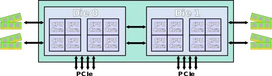
Dual-Zeppelin Configuration, as found in Ryzen Threadripper
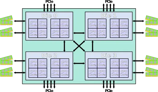
Quad-Zeppelin Configuration, as found in EPYC.


Each module consist of:
- 2 Core Complexes (CCX)
- Scalable Data Fabric (SDF)
- Memory Interface
- 2x Unified Memory Controllers (UMC) - one DRAM channel each; 64-bit data + ECC support, 2 DIMMs, DDR4 1333MT/s-3200MT/s
- PSP (MP0) and SMU (MP1) microcontrollers
- AMD Secure Processor, formerly Platform Security Processor
- System Management Unit
- NBIO
- 2 SYSHUBs, 1 IOHUB with IOMMU v2.x
- 2x8 PCIe Gen1/Gen2/Gen3
- 6 x4 PHYs plus 5 x2 PHYs
- Support PCIe, WAFL, xGMI (Inter-Chip Global Memory Interconnect), SATA, and Ethernet
- Ethernet complex: Up to 4 lanes of 10/100/1000 SGMII, or 10GBASE-KR, or 1000BASE-KX Ethernet operation
- Support PCIe, WAFL, xGMI (Inter-Chip Global Memory Interconnect), SATA, and Ethernet
- Southbridge
- ACPI, eMMC, GPIOs (6 ports), LPC, SMBus (2 ports), SPI/eSPI, UART (4 ports)
- Azalia High Definition Audio
- Up to 8 lanes of SATA Gen1/Gen2/Gen3 + legacy SATA support for SATAe
- SGPIO
- USB3.0 (4 ports of USB3 SuperSpeed)

Memory Modes[edit]
Some Zen-based models such as Ryzen Threadripper which are based on a two-Zeppelin configuration can have large variations in performance depending on how the software was designed to make use of the available memory. Threadripper offers two different memory access modes:
- UMA (Uniform Memory Access) or Distributed Mode
- NUMA (Non-uniform Memory Access) or Local Mode
The difference between the two modes is how access to the four memory controllers is done.

In UMA or Distributed Mode, memory access transactions are distributed uniformly across the four memory channels. Transactions are handled by all four channels simultaneously interleaving the distributed transactions across all channels. UMA allows applications to take advantage of the entire memory bandwidth delivered by the four memory channels. Unfortunately this means that the latency of memory access will vary depending on the path it takes, for example accesses from a channel that is physically located on the second die will be slower than local accesses. This consequently means that the average memory latency will also be slightly higher therefore applications where higher bandwidth is more important than latency will enjoy the benefits of this mode greatly.

In NUMA or Local Mode, the two local memory channels that are connected to the same die as the CPU that is executing the application is prioritized for the memory access. I.e. memory access transactions are done on the two local memory controllers that are physically located on the same die in order to deliver lower latency. In contrast to distributed mode, the total memory bandwidth is effectively halved. However this mode is important for many applications that are more sensitive to memory latency.
Accelerated Processing Units[edit]

- See also: AMD Vega and Codename Raven Ridge
In October 2017, AMD introduced the Zen-based Accelerated Processing Unit (APUs) which incorporate four "Zen" cores along with various number of Vega-based Compute Units (CUs) under the codename Raven Ridge. Zen-based APUs are based on an entirely separate die consisting of a single CCX and a GPU. It's worth noting that on this die, the CCX is configured with half the L3 cache (i.e., 1 MiB/core instead of 2). The cache amount was most likely reduced due to power constraints. The GPU is based on the Vega graphics microarchitecture featuring up to 11 Compute Units (CUs), each with 64 32-bit floating point arithmetic units. Though it's worth noting that it's currently unknown if 16-bit SIMD operations are supported like the discrete GPUs. Operating at 1 GHz, a Zen/Vega-based APU with 11 compute units will have a peak performance of 1.408 TFLOPs, likewise, the lower-end parts with just 8 CUs will have a peak performance of 1.024 TFLOPS.
Up until Zen APUs, AMD had two separate buses: Fusion Compute Link (ONION) - a coherent bus that linked the GPU and CPU together which was used for cache snooping, and a Radeon Memory Bus (GARLIC) - a non-coherent bus that linked the GPU directly to the memory controller. Starting with Zen APUs, everything is now handled by the Infinity Fabric. The desktop Zeppelin die featured a 32-byte wide data fabric, AMD has not stated if that is also the case with Raven Ridge. On Raven Ridge, the Infinity Fabric services 6 clients: CCX, GPU, Multimedia Engine, Display Engine, Memory Controller, and the I/O and System Hub. It's worth noting that unlike previous APUs, on Raven Ridge, both the Multimedia Engine and the Display Engine are now separate from the GPU and are interconnected via the fabric.
Zen-based APUs also introduced Precision Boost 2 and Mobile Extended Frequency Range (mXFR). See #Features for more details.
Power[edit]
- See also: § Power
As with the desktop parts, voltage control is done on a per-core basis with the digital Low Drop-Out (LDO) regulator. Raven Ridge extended this to the GPU as well. The regulator drops the voltage supplied to RVDD from the on-board voltage regulator module based on the highest VID. Historically, the CPU and GPU were supplied their own separate VDD. With Raven Ridge, both the CPU and GPU supply comes from a unified RVDD power rail. Power is supplied to the 4 cores and the GPU, allowing each to have their own independent P-state (i.e., voltage and frequency). Note that all the compute units in the GPU operate at the same frequency and voltage.


Enhanced power gating[edit]

Raven Ridge incorporates an enhanced power gating scheme to lower the average power consumption of the chip. Upon exiting P-State, the CPU enters the CC6 Idle State. When all the CPU cores enter CC6, the CPUOFF state is asserted and the shared L3 cache power is lowered. Likewise, when the GPU enters idle state, up to 95% of the GPU is power gated. A GPUOFF state further power down the GPU uncore. When both CPUOFF and GPUOFF states are asserted, the system VDD regulator is switched off.

Power gating on Raven Ridge is split into two regions:
- Region A - the interface between the CPU, GPU, and I/O Hub
- Region B - the memory controller, multimedia engine, and display interface
The two regions can be independently power gated depending on the workload. For example, during a typical movie playback, Region B is mostly active while Region A is mostly power gates only become briefly active when necessary.
Die[edit]
Core[edit]
There are 4 cores per CCX and 2 CCXs per die for 8 cores.
- 7 mm² area
- L2 512 KiB; 1.5 mm²/core

.png)
CCX[edit]
- 44 mm² area
- L3 8 MiB; 16 mm²
- 1,400,000,000 transistors

.png)
Memory Controller[edit]
- 15 mm²
- Two DDR4 channels
- 72-bits each

.png)
Zeppelin[edit]
- 14 nm process
- 12 metal layers
- 2,000 meters of signals
- 4,800,000,000 transistors
- ~22.058 mm x ~9.655 mm (Estimated)
- 212.97 mm² die size (note that our initial measurement from tech day was off by half a millimeter on each side)

.png)
APU[edit]
- quad-core "Zen" CPUs + "Vega" GPU with 11 CUs
- 14 nm process
- 4,950,000,000 transistors
- ~19.213 mm x ~10.919 mm (Estimated)
- 209.78 mm²

.png)
Sockets/Platform[edit]
All Zen-based mainstream consumer microprocessors utilizes AMD's Socket AM4, a unified socket infrastructure. All those processors are a complete system on a chip integrating the northbridge (memory controller) and the southbridge including 16 PCIe lanes for the GPU, 4 PCIe lanes for the NVMe/SATA controllers as well as USB 3.0. The chipset, however, extends the processor with a number of additional connections beyond that offered by the SoC.
| Socket AM4 Platform [Edit] | ||||||||||
|---|---|---|---|---|---|---|---|---|---|---|
| Segment | Chipset | USB | SATA | SATAe | PCIe | RAID | Dual PCIe | Overclocking | ||
| 3.1 G1 | 3.1 G2 | 2.0 | ||||||||
| 500-series (Zen+, Zen 2, Zen 3) | ||||||||||
| Mainstream | B550 | 2 | 6 | 6 | 8 + 4x NVME | 0 | 16x Gen4 | 0,1,10 | ✔ | ✔ |
| Enthusiast | X570 | 0 | 8 | 4 | 14 + 4x NVME | 0 | 16x Gen4 | 0,1,10 | ||
| 400-series (Zen+) | ||||||||||
| Mainstream | B450 | 2 | 2 | 6 | 6 + 4x NVME | 1 | 6x Gen3 | 0,1,10 | ✘ | ✔ |
| Enthusiast | X470 | 6 | 2 | 6 | 10 + 4x NVME | 2 | 8x Gen3 | 0,1,10 | ✔ | |
| 300-series (Zen) | ||||||||||
| Small Form Factor | A300, B300 | 4 | 0 | 0 | 2 + 2x NVMe | 1 | 4x Gen3 | 0,1 | ✘ | |
| X300 | 4 | 0 | 0 | 2 + 2x NVMe | 1 | 4x Gen3 | 0,1 | ✔ | ||
| Entry-level | A320 | 6 | 1 | 6 | 4 + 2x NVMe | 2 | 4x Gen2 | 0,1,10 | ✘ | ✘ |
| Mainstream | B350 | 6 | 2 | 6 | 4 + 2x NVMe | 2 | 6x Gen2 | 0,1,10 | ✔ | |
| Enthusiast | X370 | 6 | 2 | 6 | 6 + 2x NVMe | 2 | 8x Gen2 | 0,1,10 | ✔ | |

Threadripper uses a different socket called "Socket TR4" (or sTR4 or simply TR4). This socket allows for 4 memory channels, double the number available for Ryzen providing up to 60 PCIe lanes (64 with 4 reserved for the chipset).
| Socket TR4 Platform [Edit] | |||||||||
|---|---|---|---|---|---|---|---|---|---|
| Chipset | USB | SATA | SATAe | PCIe | RAID | Dual PCIe | Overclocking | ||
| 3.1 G1 | 3.1 G2 | 2.0 | |||||||
| X399 | 14 | 2 | 6 | 4 | 2 | 8x Gen2 | 0,1,10 | ✔ | ✔ |
Designers[edit]
- Mike Clark, chief architect
Bibliography[edit]
- IEEE Hot Chips 28 Symposium (HCS) 2016
- AMD x86 Memory Encryption Technologies, Linux Security Summit 2016, David Kaplan, Security Architect, August 25, 2016
- Lisa Su, AMD CEO, AMD: New Horizon Live Event
- Lisa Su, AMD CEO, AMD Annual Meeting of Shareholders Q4 2016
- Meet the AMD Experts - AMD Monthly Partner Training, January 2017
- IEEE ISSCC 2017
- AMD 'Tech Day', February 22, 2017
- AMD Infinity Fabric introduction by Mark Papermaster, April 6, 2017
- AMD Zen at GDC 2017, March 3, 2017
- AMD 2017 Financial Analyst Day, May 16, 2017
- AMD EPYC Tech Day, June 20, 2017
- IEEE Hot Chips 29 Symposium (HCS) 2017
- AMD Ryzen Processor With Radeon Vega Graphics, October, 2017
- IEEE ISSCC 2018
- Processor Programming Reference (PPR) for AMD Family 17h Model 01h, Revision B1 Processors
Documents[edit]
- AMD Ryzen CPU Optimization
- AMD Ryzen processors Master Overclocking User Guide
- AMD Financial Analyst Day 2017 - Datacenter
- AMD EPYC
- AMD EPYC 7000-series Product Brief, June 2017
- AMD EPYC Performance Brief, June 2017
- AMD EPYC Solution Brief, June 2017
- AMD x86 Memory Encryption Technologies, David Kaplan, Security Architect, LSS 2016 August 25, 2016
Manuals[edit]
See also[edit]
|
|
|
|
|
. |
| codename | Zen + |
| core count | 4 +, 6 +, 8 +, 12 +, 16 +, 24 + and 32 + |
| designer | AMD + |
| first launched | March 2, 2017 + |
| full page name | amd/microarchitectures/zen + |
| instance of | microarchitecture + |
| instruction set architecture | x86-64 + |
| manufacturer | GlobalFoundries + |
| microarchitecture type | CPU + |
| name | Zen + |
| pipeline stages | 19 + |
| process | 14 nm (0.014 μm, 1.4e-5 mm) + |