Static random-access memory (Static RAM or SRAM) is a simple semiconductor memory device that implements a random-access memory-based storage that holds data in a static form. That is, static RAM retains its data for as long as the memory device has power. SRAM is the most common type of memory cell found in most VLSI designs.
Contents
Overview[edit]
Static Random Access Memory (SRAM) is a type of semiconductor memory. It is static and volatile, implying data retention persists for as long as the device is powered without any form of a refresh, however, once the power is cut, data will be lost. It is random access, meaning the next memory location that can be read or written to does not depend on the last access location. The static property of SRAM comes from its use of some sort of a feedback mechanism to maintain the stored bit state. This is in contrast to other forms of memory, such as Dynamic RAM, where the stored state of the bit is kept in the form of a charge that leaks over time thereby requiring the data to be refreshed (i.e, read and re-written back).
Large blocks of SRAM memory comprise of arrays of individual SRAM blocks called cells. An SRAM cell is capable of storing a single bit of data for as long as there is power. Likewise, an array of eight SRAM cells can store 1 byte of data. Arrays of SRAM form the foundation for every
Applications[edit]
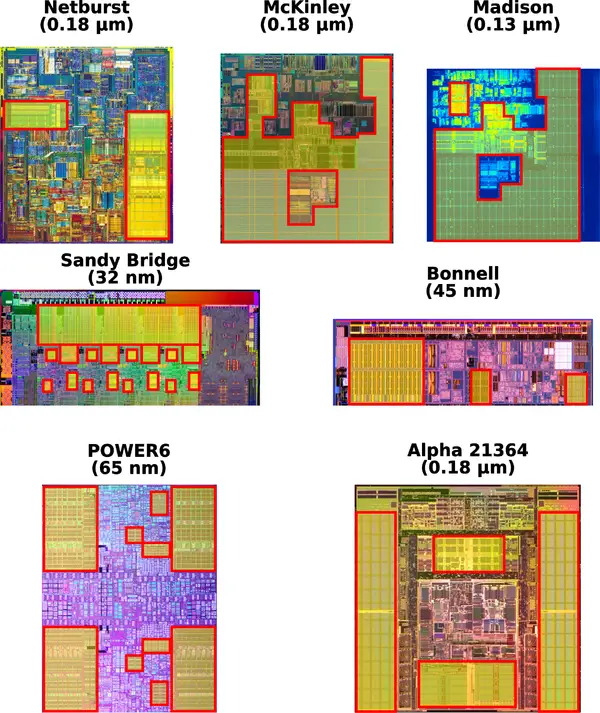
Due to its relative simplicity, SRAM is the most common memory cell found in modern microprocessors. It is used for various large buffers and caches. Current SoCs allocate a large portion of the die to SRAM. For example, in Intel's first-generation Atom processors, codename Bonnell, 30,644,682 out of the 47,212,207 transistors (65%) were dedicated to the level 2 cache. In Intel's Itanium 2, codename Montecito, 90% of the 1.72-billion transistors were occupied by SRAM.
Below are large SRAM blocks highlighted on real-world high-performance microprocessors, showing how much silicon area, SRAM typically occupies. There are many smaller blocks that were not marked.
- Note: Die images NOT to scale.
Operation[edit]
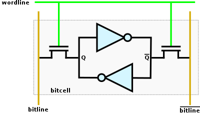
Static RAMs use basic memory cells with built-in feedback mechanisms that retain the stored value for as long as the device is powered. A basic example of a feedback mechanism is a pair of inverters that are cross-coupled such that the output of one inverter becomes the input of the other inverter. As long as there is power, the stored value will be continuously reinforced by the positive feedback loop which also helps correct for leakage and noise.
Writing a new bit value involves driving the desired value and its complement onto the input and output of the cross-coupled inverters. By driving a stronger new value and overpowering the older values, a new bit value may be stored in the cell.
Reading the stored value involves reading the output of the cell. Note that in practice, due to the size of the transistors involved which makes them very weak, driving the output directly from the bitcell is very challenging. Instead, a sense amplifier is used to generate a strong output from the attenuated bit value. This is explained in more detail later in this article.
Bit Cells[edit]
The SRAM bitcell is the basic building block of SRAM memory. A cell holds a single bit value for as long as there is power. The two access points to the cell are known as bitlines (BL). The bitlines comprise of the stored bit value and its complement. Two access transistors sit on the bitlines in order to enable and disable access to the stored data for reading and writing operations. The signal that controls the access transistors is referred to as a wordline (WL).
6T Cell[edit]
The most common implementation of an SRAM bitcell is the 6-transistor bitcell (6T cell). This cell comprises a pair of weak cross-coupled CMOS inverters and a pair of access transistors used for reading and writing the stored state. 6T cells can provide excellent noise margins and low leakage with relatively good density. Because the transistors are very small and thus weak, more complex assist circuits are required for reading and writing the cells.
4T Cell[edit]
A 4-transistor bitcell (4T cell) is a modified version of the 6T cell with the two PMOS pull-up transistors removed. This design sacrifices static power dissipation in favor of higher density. In this configuration, the two PMOS transistors are replaced with denser high resistance resistors.
8T Cell[edit]
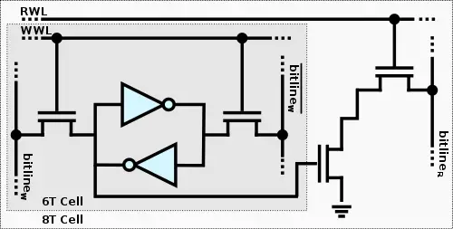
An 8-transistor bitcell (8T cell) is an enhanced version of the 6T cell which decouples the read port from the write port. A new read buffer comprising 2 nMOS transistors is added to the 6T cell.
This has a number of performance advantages. By decoupling the read from write, the read SNM is drastically reduced. Additionally, both the read and write performance can be optimized individually by adjusting the 6T cell part separately from the read buffer size. In other words, the decoupled read buffer permits lower write voltages while enabling higher read currents.
Leading-edge SRAM[edit]
| This section is empty; you can help add the missing info by editing this page. |


