(→Documents) |
(fixed) |
||
| (4 intermediate revisions by 4 users not shown) | |||
| Line 1: | Line 1: | ||
{{Lithography processes}} | {{Lithography processes}} | ||
| − | The '''45 nanometer (45 nm) lithography process''' is a [[technology node|full node]] semiconductor manufacturing process following the [[55 nm lithography process|55 nm process]] stopgap. Commercial [[integrated circuit]] manufacturing using 45 nm process began in 2007. This technology was superseded by the [[40 nm lithography process|40 nm | + | The '''45 nanometer (45 nm) lithography process''' is a [[technology node|full node]] semiconductor manufacturing process following the [[55 nm lithography process|55 nm process]] stopgap. |
| + | :Commercial [[integrated circuit]] manufacturing using [[45 nm]] process began in [[2007]]. | ||
| + | This technology was superseded by the [[40 nm lithography process|40 nm]] (HN) / [[32 nm lithography process|32 nm process]] (FN) in [[2010]]. | ||
== Industry == | == Industry == | ||
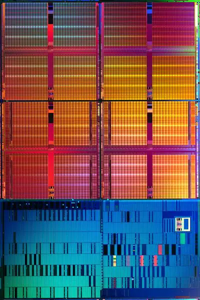
| − | In January of 2006 Intel announced that they've been able to fabricate the first fully functional [[SRAM]] chips on a 45 nm process. As a preview Intel showcased | + | [[File:45nm SRAM photo.JPG|left|400px|Die photo of an [[Intel]] [[45 nm]] shuttle test chip including 153 MiB [[SRAM]] and logic test circuits]] |
| − | {{scrolling table/top|style=text-align: right; | first=Fab | + | In January of [[2006]] [[Intel]] announced that they've been able to fabricate the first fully functional [[SRAM]] chips on a [[45 nm]] process. As a preview Intel showcased 45 nm SRAM chip (shown below) packing more than 1 billion transistors. Intel opened 3 45 nm facilities, their initial {{intel|D1D}} facility in Oregon, {{intel|Fab 32}} in Arizona and {{intel|Fab 28}} in Israel. Intel's 45 nm process is the first time high-k + metal gate transistors was used in high-volume manufacturing process. |
| − | |Process Name | + | |
| + | {| class="wikitable" | ||
| + | |- | ||
| + | ! colspan="4" | [[Intel]] 45 nm Design Rules | ||
| + | |- | ||
| + | ! Layer !! Pitch !! Thick !! Aspect <br>Ratio | ||
| + | |- | ||
| + | | Isolation || 200 nm || 200 nm || - | ||
| + | |- | ||
| + | | Contacted <br>Gate || 180 nm || 60 nm || -- | ||
| + | |- | ||
| + | | Metal 1 || 160 nm || 144 nm || 1.8 | ||
| + | |- | ||
| + | | Metal 2 || 160 nm || 144 nm || 1.8 | ||
| + | |- | ||
| + | | Metal 3 || 160 nm || 144 nm || 1.8 | ||
| + | |- | ||
| + | | Metal 4 || 240 nm || 216 nm || 1.8 | ||
| + | |- | ||
| + | | Metal 5 || 280 nm || 252 nm || 1.8 | ||
| + | |- | ||
| + | | Metal 6 || 360 nm || 324 nm || 1.8 | ||
| + | |- | ||
| + | | Metal 7 || 560 nm || 504 nm || 1.7 | ||
| + | |- | ||
| + | | Metal 8 || 810 nm || 720 nm || 1.8 | ||
| + | |- | ||
| + | | Metal 9 || 30.5 µm || 7 µm || 0.4 | ||
| + | |} | ||
| + | |||
| + | === Specifications === | ||
| + | {{scrolling table/top|style=text-align: right; | first=Fab /<br>Manuf | ||
| + | |Process <br>Name | ||
|1st Production | |1st Production | ||
|Type | |Type | ||
| Line 18: | Line 52: | ||
{{scrolling table/mid}} | {{scrolling table/mid}} | ||
|- | |- | ||
| − | ! colspan="2" | [[Intel]] !! colspan="2" | [[Fujitsu]] !! colspan="2" | [[TI]] !! colspan="2" | [[Toshiba]] / [[Sony]] / [[NEC]] !! colspan="2" | [[Samsung]] !! colspan="2" | [[IBM]] / [[Toshiba]] / [[Sony]] / [[AMD]] | + | ! colspan="2" | [[Intel]] !! colspan="2" | [[Fujitsu]] !! colspan="2" | [[TI]] !! colspan="2" | [[Toshiba]] / <br>[[Sony]] / [[NEC]] !! colspan="2" | [[Samsung]] !! colspan="2" | [[IBM]] / [[Toshiba]] / <br>[[Sony]] / [[AMD]] |
|- style="text-align: center;" | |- style="text-align: center;" | ||
| − | | colspan="2" | P1266 (CPU) / | + | | colspan="2" | P1266 (CPU) / P1269 (SoC) <br>/ P1266.8 (SoC) || colspan="2" | CS-300 || colspan="2" | || colspan="2" | || colspan="2" | 11LP || colspan="2" | |
|- style="text-align: center;" | |- style="text-align: center;" | ||
| colspan="2" | 2006 || colspan="2" | 2008 || colspan="2" | 2008 || colspan="2" | 2006 || colspan="2" | 2007 || colspan="2" | 2007 | | colspan="2" | 2006 || colspan="2" | 2008 || colspan="2" | 2008 || colspan="2" | 2006 || colspan="2" | 2007 || colspan="2" | 2007 | ||
| Line 40: | Line 74: | ||
| || || || || || || || || 0.11 µm² || 0.58x || 0.067 µm² || 0.53x | | || || || || || || || || 0.11 µm² || 0.58x || 0.067 µm² || 0.53x | ||
{{scrolling table/end}} | {{scrolling table/end}} | ||
| + | |||
=== Intel === | === Intel === | ||
<gallery widths=200px heights=300px> | <gallery widths=200px heights=300px> | ||
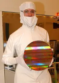
| − | File:45nm | + | File:45nm wafer photo 2.JPG|Intel engineer holding 300 mm wafer with 45 nm shuttle test chips |
| − | |||
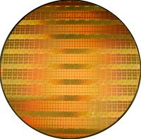
File:45nm wafer photo 1.jpg|300 mm wafer with 45 nm shuttle test chips | File:45nm wafer photo 1.jpg|300 mm wafer with 45 nm shuttle test chips | ||
| − | |||
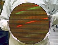
File:45nm-wafer-photo-3.jpg|Intel 300 mm wafer with 45 nm shuttle test chips | File:45nm-wafer-photo-3.jpg|Intel 300 mm wafer with 45 nm shuttle test chips | ||
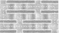
| + | File:45nm SRAM Cell.jpg|6T SRAM Bit-Cell | ||
</gallery> | </gallery> | ||
| − | |||
| − | |||
| − | |||
| − | |||
| − | |||
| − | |||
| − | |||
| − | |||
| − | |||
| − | |||
| − | |||
| − | |||
| − | |||
| − | |||
| − | |||
| − | |||
| − | |||
| − | |||
| − | |||
| − | |||
| − | |||
| − | |||
| − | |||
| − | |||
| − | |||
| − | |||
| − | |||
| − | |||
| − | |||
== 45 nm Microprocessors== | == 45 nm Microprocessors== | ||
| Line 83: | Line 88: | ||
** {{amd|Opteron}} | ** {{amd|Opteron}} | ||
** {{amd|Phenom II}} | ** {{amd|Phenom II}} | ||
| + | * Freescale | ||
| + | ** {{freescale|QorIQ}} | ||
* IBM | * IBM | ||
** {{ibm|Power7}} | ** {{ibm|Power7}} | ||
| Line 105: | Line 112: | ||
== 45 nm Microarchitectures == | == 45 nm Microarchitectures == | ||
| + | * AMD | ||
| + | ** {{amd|K10|l=arch}} | ||
| + | * IBM | ||
| + | ** {{ibm|z196|l=arch}} | ||
* Intel | * Intel | ||
| − | ** {{intel| | + | ** {{intel|Bonnell|l=arch}} |
| − | ** {{intel| | + | ** {{intel|Nehalem|l=arch}} |
| − | ** {{intel| | + | ** {{intel|Penryn|l=arch}} |
| − | * | + | * VIA Technologies |
| − | ** {{ | + | ** {{via|Isaiah|l=arch}} |
{{expand list}} | {{expand list}} | ||
| Line 123: | Line 134: | ||
== References == | == References == | ||
* Mistry, Kaizad, et al. "A 45nm logic technology with high-k+ metal gate transistors, strained silicon, 9 Cu interconnect layers, 193nm dry patterning, and 100% Pb-free packaging." Electron Devices Meeting, 2007. IEDM 2007. IEEE International. IEEE, 2007. | * Mistry, Kaizad, et al. "A 45nm logic technology with high-k+ metal gate transistors, strained silicon, 9 Cu interconnect layers, 193nm dry patterning, and 100% Pb-free packaging." Electron Devices Meeting, 2007. IEDM 2007. IEEE International. IEEE, 2007. | ||
| + | |||
| + | [[category:lithography]] | ||
Latest revision as of 20:39, 19 March 2025
The 45 nanometer (45 nm) lithography process is a full node semiconductor manufacturing process following the 55 nm process stopgap.
- Commercial integrated circuit manufacturing using 45 nm process began in 2007.
This technology was superseded by the 40 nm (HN) / 32 nm process (FN) in 2010.
Contents
Industry[edit]
In January of 2006 Intel announced that they've been able to fabricate the first fully functional SRAM chips on a 45 nm process. As a preview Intel showcased 45 nm SRAM chip (shown below) packing more than 1 billion transistors. Intel opened 3 45 nm facilities, their initial D1D facility in Oregon, Fab 32 in Arizona and Fab 28 in Israel. Intel's 45 nm process is the first time high-k + metal gate transistors was used in high-volume manufacturing process.
| Intel 45 nm Design Rules | |||
|---|---|---|---|
| Layer | Pitch | Thick | Aspect Ratio |
| Isolation | 200 nm | 200 nm | - |
| Contacted Gate |
180 nm | 60 nm | -- |
| Metal 1 | 160 nm | 144 nm | 1.8 |
| Metal 2 | 160 nm | 144 nm | 1.8 |
| Metal 3 | 160 nm | 144 nm | 1.8 |
| Metal 4 | 240 nm | 216 nm | 1.8 |
| Metal 5 | 280 nm | 252 nm | 1.8 |
| Metal 6 | 360 nm | 324 nm | 1.8 |
| Metal 7 | 560 nm | 504 nm | 1.7 |
| Metal 8 | 810 nm | 720 nm | 1.8 |
| Metal 9 | 30.5 µm | 7 µm | 0.4 |
Specifications[edit]
| Fab / Manuf |
|---|
| Process Name |
| 1st Production |
| Type |
| Wafer |
| |
| Contacted Gate Pitch |
| Interconnect Pitch (M1P) |
| SRAM bit cell (HD) |
| SRAM bit cell (LP) |
| DRAM bit cell |
| Intel | Fujitsu | TI | Toshiba / Sony / NEC |
Samsung | IBM / Toshiba / Sony / AMD | ||||||
|---|---|---|---|---|---|---|---|---|---|---|---|
| P1266 (CPU) / P1269 (SoC) / P1266.8 (SoC) |
CS-300 | 11LP | |||||||||
| 2006 | 2008 | 2008 | 2006 | 2007 | 2007 | ||||||
| Bulk | PDSOI | ||||||||||
| 300mm | |||||||||||
| Value | 65 nm Δ | Value | 65 nm Δ | Value | 65 nm Δ | Value | 65 nm Δ | Value | 65 nm Δ | Value | 65 nm Δ |
| 180 nm | 0.82x | 190 nm | ?x | ? nm | ?x | 180 nm | ?x | ? nm | ?x | 190 nm | 0.76x |
| 160 nm | 0.76x | ? nm | ?x | ? nm | ?x | ? nm | ?x | ? nm | ?x | ? nm | ?x |
| 0.346 µm² | 0.61x | 0.225 µm² | ?x | 0.255 µm² | ?x | 0.248 µm² | ?x | 0.29 µm² | 0.54x | 0.370 µm² | 0.57x |
| 0.3816 µm² | 0.56x | 0.359 µm² | 0.53x | ||||||||
| 0.11 µm² | 0.58x | 0.067 µm² | 0.53x | ||||||||
Intel[edit]
45 nm Microprocessors[edit]
- AMD
- Freescale
- IBM
- Intel
This list is incomplete; you can help by expanding it.n Chips== This list is incomplete; you can help by expanding it.
45 nm Microarchitectures[edit]
This list is incomplete; you can help by expanding it.
Documents[edit]
References[edit]
- Mistry, Kaizad, et al. "A 45nm logic technology with high-k+ metal gate transistors, strained silicon, 9 Cu interconnect layers, 193nm dry patterning, and 100% Pb-free packaging." Electron Devices Meeting, 2007. IEDM 2007. IEEE International. IEEE, 2007.
 Semiconductor lithography processes technology
