Semiconductor & Computer Engineering
 Semiconductor lithography processes technology
The 45 nanometer (45 nm) lithography process is a full node semiconductor manufacturing process following the 55 nm process stopgap.
- Commercial integrated circuit manufacturing using 45 nm process began in 2007.
This technology was superseded by the 40 nm (HN) / 32 nm process (FN) in 2010.
Contents
Industry[edit]

In January of 2006 Intel announced that they've been able to fabricate the first fully functional SRAM chips on a 45 nm process. As a preview Intel showcased 45 nm SRAM chip (shown below) packing more than 1 billion transistors. Intel opened 3 45 nm facilities, their initial D1D facility in Oregon, Fab 32 in Arizona and Fab 28 in Israel. Intel's 45 nm process is the first time high-k + metal gate transistors was used in high-volume manufacturing process.
| Intel 45 nm Design Rules | |||
|---|---|---|---|
| Layer | Pitch | Thick | Aspect Ratio |
| Isolation | 200 nm | 200 nm | - |
| Contacted Gate |
180 nm | 60 nm | -- |
| Metal 1 | 160 nm | 144 nm | 1.8 |
| Metal 2 | 160 nm | 144 nm | 1.8 |
| Metal 3 | 160 nm | 144 nm | 1.8 |
| Metal 4 | 240 nm | 216 nm | 1.8 |
| Metal 5 | 280 nm | 252 nm | 1.8 |
| Metal 6 | 360 nm | 324 nm | 1.8 |
| Metal 7 | 560 nm | 504 nm | 1.7 |
| Metal 8 | 810 nm | 720 nm | 1.8 |
| Metal 9 | 30.5 µm | 7 µm | 0.4 |
Specifications[edit]
| Fab / Manuf |
|---|
| Process Name |
| 1st Production |
| Type |
| Wafer |
| |
| Contacted Gate Pitch |
| Interconnect Pitch (M1P) |
| SRAM bit cell (HD) |
| SRAM bit cell (LP) |
| DRAM bit cell |
| Intel | Fujitsu | TI | Toshiba / Sony / NEC |
Samsung | IBM / Toshiba / Sony / AMD | ||||||
|---|---|---|---|---|---|---|---|---|---|---|---|
| P1266 (CPU) / P1269 (SoC) / P1266.8 (SoC) |
CS-300 | 11LP | |||||||||
| 2006 | 2008 | 2008 | 2006 | 2007 | 2007 | ||||||
| Bulk | PDSOI | ||||||||||
| 300mm | |||||||||||
| Value | 65 nm Δ | Value | 65 nm Δ | Value | 65 nm Δ | Value | 65 nm Δ | Value | 65 nm Δ | Value | 65 nm Δ |
| 180 nm | 0.82x | 190 nm | ?x | ? nm | ?x | 180 nm | ?x | ? nm | ?x | 190 nm | 0.76x |
| 160 nm | 0.76x | ? nm | ?x | ? nm | ?x | ? nm | ?x | ? nm | ?x | ? nm | ?x |
| 0.346 µm² | 0.61x | 0.225 µm² | ?x | 0.255 µm² | ?x | 0.248 µm² | ?x | 0.29 µm² | 0.54x | 0.370 µm² | 0.57x |
| 0.3816 µm² | 0.56x | 0.359 µm² | 0.53x | ||||||||
| 0.11 µm² | 0.58x | 0.067 µm² | 0.53x | ||||||||
Intel[edit]
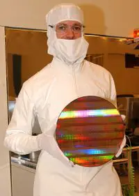
Intel engineer holding 300 mm wafer with 45 nm shuttle test chips
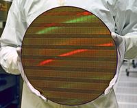
300 mm wafer with 45 nm shuttle test chips
Intel 300 mm wafer with 45 nm shuttle test chips
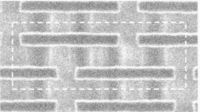
6T SRAM Bit-Cell


45 nm Microprocessors[edit]
- AMD
- Freescale
- IBM
- Intel
This list is incomplete; you can help by expanding it.n Chips== This list is incomplete; you can help by expanding it.
45 nm Microarchitectures[edit]
This list is incomplete; you can help by expanding it.
Documents[edit]
References[edit]
- Mistry, Kaizad, et al. "A 45nm logic technology with high-k+ metal gate transistors, strained silicon, 9 Cu interconnect layers, 193nm dry patterning, and 100% Pb-free packaging." Electron Devices Meeting, 2007. IEDM 2007. IEEE International. IEEE, 2007.