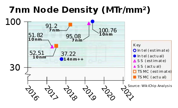
The 7 nanometer (7 nm) lithography process is a technology node semiconductor manufacturing process following the 10 nm process node. Mass production of integrated circuit fabricated using a 7 nm process begun in 2018. The process technology will be phased out by leading-edge foundries by 2020/21 timeframe where it will be replaced by the 5 nm node.
The term "7 nm" is simply a commercial name for a generation of a certain size and its technology, and does not represent any geometry of the transistor.
Contents
Overview
First introduced by the major foundries around the 2018-19 timeframe, the 7-nanometer process technology is characterized by its use of FinFET transistors with fin pitches in the 30s of nanometer and densest metal pitches in the upper 30s or low 40s of nanometers. Due to the small feature sizes, quad patterning had to be utilized for some layers. This process was introduced just as EUV Lithography became ready for mass production, therefore some foundries utilized EUV while others didn't. Note that Intel 10 nm process is comparable to the foundry 7-nanometer node.
Density
In terms of raw cell-level density, the 7-nanometer node features silicon densities between 90-105 million transistors per square millimeter based on WikiChip's own analysis.
Industry
Only three companies are currently planning or developing a 5-nanometer node: Intel, TSMC, and Samsung.
| Intel | TSMC | Samsung | GlobalFoundries | ||||||
|---|---|---|---|---|---|---|---|---|---|
| Process | P1276 (CPU), P1277 (SoC) | N7, N7P, N7+ | 7LPE, 7LPP | ||||||
| Production | 2021 | April 2018 | April 2019 | Cancelled | |||||
| Litho | Lithography | EUV | DUV ⇒ EUV | EUV | DUV ⇒ EUV | ||||
| Immersion Exposure | SADP ⇒ SE (EUV) DP (193i) | SE (EUV) DP (193i) | SADP ⇒ SE (EUV) DP (193i) | ||||||
| Wafer | Type | Bulk | |||||||
| Size | 300 mm | ||||||||
| xTor | Type | FinFET | |||||||
| Voltage | |||||||||
| Value | 10 nm Δ | Value | 10 nm Δ | Value | 10 nm Δ | Value | 14 nm Δ | ||
| Fin | Pitch | 30 nm | 0.83x | 27 nm | 0.64x | 30 nm | 0.625x | ||
| Width | 6 nm | 1.00x | |||||||
| Height | 52 nm | 1.24x | |||||||
| Gate Length (Lg) | 8/10 nm | ||||||||
| Contacted Gate Pitch (CPP) | 64 nm (HP) 57 nm (HD) | 0.82x | 60 nm (HP) 54 nm (HD) | 0.79x | 56 nm | 0.72x | |||
| Minimum Metal Pitch (MMP) | 40 nm | 0.95x | 36 nm | 0.75x | 40 nm | 0.625x | |||
| SRAM | High-Perf (HP) | 0.032 µm² | 0.65x | 0.0353 µm² | 0.44x | ||||
| High-Density (HD) | 0.027 µm² | 0.64x | 0.026 µm² | 0.65x | 0.0269 µm² | 0.42x | |||
| Low-Voltage (LV) | |||||||||
Intel
P1276
Intel's 7-nanometer process, P1276, will enter risk production at the end of 2020 and ramp in 2021. On February 8 2017 Intel announced a $7B investment in Arizona's Fab 42 which will eventually produce chips on a 7 nm process.
Intel has not disclosed the details of the process but the company's current CEO claims it will feature a density that is 2x that of Intel's 10-nanometer node. Intel's prior CEO, Brian Krzanich, mentioned that 7-nanometer will have "2.4x the compaction ratio" of 10 nm. This puts the 7-nanometer node at around 202-250 transistors per square millimeter.
TSMC
N7
N7P
Samsung
7LPE
7LPP
GlobalFoundries
7LP
7HPC
7 nm Microprocessors
- PEZY
- MediaTek
- Apple
- HiSilicon (Huawei)
- Snapdragon (Qualcomm)
This list is incomplete; you can help by expanding it.
7 nm Microarchitectures
- AMD
- Ampere
- Esperanto
- Intel
 Semiconductor lithography processes technology
