From WikiChip
Difference between revisions of "32 nm lithography process"
(→Industry) |
|||
| Line 17: | Line 17: | ||
| process 1 transistor = Planar | | process 1 transistor = Planar | ||
| process 1 volt = | | process 1 volt = | ||
| + | | process 1 layers = 9 | ||
| process 1 delta from = [[45 nm]] Δ | | process 1 delta from = [[45 nm]] Δ | ||
| process 1 gate len = | | process 1 gate len = | ||
Revision as of 19:59, 5 April 2017
The 32 nanometer (32 nm) lithography process is a full node semiconductor manufacturing process following the 40 nm process stopgap. Commercial integrated circuit manufacturing using 32 nm process began in 2010. This technology was superseded by the 28 nm process (HN) / 22 nm process (FN) in 2012.
Contents
Industry
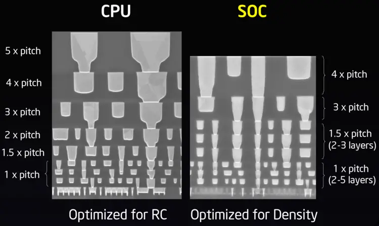
TSMC cancelled its planned 32nm node process. Intel's 32 nm process became the first process to introduce the self-aligned via patterning.
| Process Name | |
|---|---|
| 1st Production | |
| Litho- graphy |
Lithography |
| Immersion | |
| Exposure | |
| Wafer | Type |
| Size | |
| Tran- sistor |
Type |
| Voltage | |
| Metal Layers | |
| Gate Length (Lg) | |
| Contacted Gate Pitch (CPP) | |
| Minimum Metal Pitch (MMP) | |
| SRAM bitcell |
High-Perf (HP) |
| High-Density (HD) | |
| Low-Voltage (LV) | |
| DRAM bitcell |
eDRAM |
| Intel | |
|---|---|
| P1268 (CPU) / P1269 (SoC) | |
| 2009 | |
| 193 nm | |
| Yes | |
| SADP | |
| Bulk | |
| 300 mm | |
| Planar | |
| 9 | |
| Value | 45 nm Δ |
| 112.5 nm | 0.63x |
| 112.5 nm | 0.70x |
| 0.148 µm2 | 0.43x |
| 0.199 µm2 | |
| 0.171 µm2 | 0.45x |
| Fab |
|---|
| Process Name |
| 1st Production |
| Type |
| Wafer |
| |
| Contacted Gate Pitch |
| Interconnect Pitch (M1P) |
| SRAM bit cell (HD) |
| SRAM bit cell (HS) |
| SRAM bit cell (LP) |
| DRAM bit cell |
| Common Platform | TSMC | Samsung | Toshiba / NEC | Common Platform 2 | |||||||
|---|---|---|---|---|---|---|---|---|---|---|---|
| 32LP | |||||||||||
| 2009 | 2009 | 2009 | 2009 | 2010 | |||||||
| PDSOI | Bulk | ||||||||||
| 300mm | |||||||||||
| Value | 45 nm Δ | Value | 40 nm Δ | Value | 40 nm Δ | Value | 40 nm Δ | Value | 45 nm Δ | ||
| 130 nm | 0.68x | 130 nm | 0.80x | 126 nm | 0.98x | 120 nm | 0.71x | 126 nm | 0.66x | ||
| ? nm | ?x | 100 nm | 0.83x | 100 nm | 0.85x | ? nm | ?x | 100 nm | ?x | ||
| 0.15 µm2 | 0.41x | 0.15 µm2 | 0.62x | 0.149 µm2 | ?x | 0.124 µm2 | 0.64x | 0.157 µm2 | 0.42x | ||
| 0.039 µm2 | 0.58x | ||||||||||
Design Rules
Find models
Click to browse all 32 nm MPU models
32 nm Microprocessors
- AMD
- Intel
- UC Davis
- Princeton
This list is incomplete; you can help by expanding it.
32 nm Microarchitectures
- Intel
- AMD
This list is incomplete; you can help by expanding it.
References
- Samsung foundry solution for 32 & 28 nm
- Diaz, C. H., et al. "32nm gate-first high-k/metal-gate technology for high performance low power applications." Electron Devices Meeting, 2008. IEDM 2008. IEEE International. IEEE, 2008.
 Semiconductor lithography processes technology
