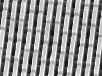
(→10 nm process nodes) |
|||
| (16 intermediate revisions by 13 users not shown) | |||
| Line 8: | Line 8: | ||
At the advanced 10nm process, there are only 3 semiconductor foundries with such manufacturing capabilities: [[Intel]], [[Samsung]], and [[TSMC]]. | At the advanced 10nm process, there are only 3 semiconductor foundries with such manufacturing capabilities: [[Intel]], [[Samsung]], and [[TSMC]]. | ||
| − | Due to marketing names, geometries vary greatly between leading | + | Due to marketing names, geometries vary greatly between leading manufacturers. Although both TSMC and Samsung's 10nm processes are slightly denser than Intel's 14nm in raw logic density, they are far closer to Intel's 14nm than they are to Intel's 10nm (e.g., Samsung's metal pitch just 1 nanometer shorter than Intel's 14nm). |
| + | === Intel === | ||
| + | {{see also|intel/process|l1=Intel's Process Technology History}} | ||
| + | [[File:intel 10nm fin.png|left|200px]] | ||
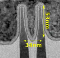
| + | Announced during Intel's Technology and Manufacturing Day 2017, Intel's 10 nm process (P1274) is Intel's first high-volume manufacturing process to employ [[Self-Aligned Quad Patterning]] (SAQP) with production starting in the second half of 2017. Intel detailed {{intel|Hyper-Scaling}}, a marketing term for a suite of techniques used to [[transistor scaling|scale a transistor]], SAQP, a single dummy gate and [[contact over active gate]] (COAG). Intel's initial 10 nm process has up to 60% lower power and 25% better performance than their initial 14 nm but will actually have lower performance than their "14nm++" process. Intel expect their "10nm+" process to surpass that. | ||
| + | |||
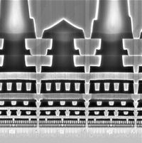
| + | Intel's 10nm process is roughly 1.7x the raw logic density of the next densest 10nm process, albeit due to aggressive pattering techniques they also have the most complex process available to date. The process can support multiple threshold voltages, and features 12-metal interconnect layers with the bottom two made of cobalt. This is the first time cobalt is used in a high volume production node. Because of the ever shrinking geometries the wires get smaller each node. | ||
| + | [[File:intel interconnect 10 nm.jpg|left|200px]] | ||
| + | At 10nm the wires become so small that the barrier layer takes up most of the interconnect, resulting in less space for the copper itself. As the cross section of the wire gets smaller the resistance rises exponentially. Cobalt aims to address this issue, it does not diffuse in the surrounding material, so the barrier layer can be reduced. And even though it has a higher resistance than copper in bulk, it has up to two times lower resistance in very small wires. This can be attributed to the larger wires because of the reduced barrier layer and the larger grain size, which reduces the electron scattering. It also has 10x better resistance to electron-migration. | ||
| + | |||
| + | Intel will leverage their initial 10nm process for their {{intel|Cannon Lake|l=arch}}-based microprocessors which are used exclusively for mobile. They will then utilize their second generation, "10nm+" process, for {{intel|Ice Lake|l=arch}}-based processors which will be used for the mainstream and server platform. | ||
| + | |||
| + | ===== Intel 7 Ultra ===== | ||
| + | [[File:raptor-lake-v-f-curve-improvements.png|thumb|left|New V-F Curve for the Enhanced Intel 7 process.]] | ||
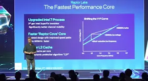
| + | Intel introduced an '''enhanced version of the Intel 7 process''' in late 2022 with the introduction of the company's 13th Generation Core processors based on the {{intel|Raptor Lake|l=arch}} microarchitecture. Nicknamed '''"Intel 7 Ultra"''' internally, the new process is a full PDK update over the one used by Alder Lake, their 3rd generation SuperFin Transistor architecture. Intel says this process brings transistors with significantly better channel mobility. At the very high end of the V-F curve, the company says peak frequency is nearly 1 GHz higher now. The curve itself has been improved, shifting prior-generation frequencies by around 200 MHz at ISO-voltage, or alternatively, reducing the voltage by over 50 mV at ISO-frequency. | ||
| + | |||
| + | * [https://fuse.wikichip.org/news/525/iedm-2017-isscc-2018-intels-10nm-switching-to-cobalt-interconnects/ In-depth analysis for Intel's 10nm process.] | ||
| + | {{clear}} | ||
| + | |||
| + | === Samsung === | ||
| + | [[File:ss 14-10nm.png|right|500px]] | ||
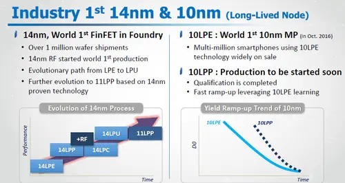
| + | Samsung demonstrated their 128 Megabit [[SRAM]] wafer from their 10nm FinFET process. Samsung, which unlike Intel uses LELELE (litho-etch-litho-etch-litho-etch), ramped up mass production in May of 2017. ChipWorks/TechInsight measured the CPP/MMP which came a little short of the Common Platform Alliance Paper which was presented in 2016, at 68 nm contacted gate pitch, 51 nm metal pitch, dual-depth [[shallow trench isolation]] (STI), and had single dummy gate. | ||
| + | |||
| + | Samsung's initial process was 10LPE (10 Low-Power Early) which was replaced by second generation evolved process 10LPP (10 Low-Power Plus). Samsung intends to introduce a third generational enhanced 10nm process called 8LPP (8 Low Power Plus) which will further improve performance and introduce a small density increase through cell enhancements and a narrower metal pitch. 8LPP improvements over 10LPP is similar to their 11LPP improvements over their 14LPP. It's worth noting that Samsung intends 8LPP to be their last non-[[EUV]] node. All subsequent nodes will use EUV. | ||
| + | |||
| + | [[File:10nm tsmc.jpeg|right|200px]] | ||
| + | |||
| + | {| class="collapsible collapsed wikitable" | ||
| + | |- | ||
| + | ! colspan="2" | Samsung 128 Mib SRAM demo 10 nm wafer | ||
| + | |- | ||
| + | | | ||
| + | <table class="wikitable"> | ||
| + | <tr><th>Technology</th><td>10nm FinFET</td></tr> | ||
| + | <tr><th>Supply voltage</th><td>1.8 V (i/o)</td></tr> | ||
| + | <tr><th>Bit cell size</th><td>0.040 µm²</td></tr> | ||
| + | <tr><th>macro configs</th><td>256x512 Kib</td></tr> | ||
| + | <tr><th>Capacity</th><td>128 Mib</td></tr> | ||
| + | <tr><th>Test Features</th><td>Programmable E-fuse</td></tr> | ||
| + | <tr><th>Die Size</th><td>75.6mm²</td></tr> | ||
| + | </table> | ||
| + | | [[File:samsung 10nm SRAM block.png|400px]] | ||
| + | |} | ||
| + | |||
| + | === TSMC === | ||
| + | TSMC reported a poly pitch of 64 nm with a metal pitch 42 nm. TechInsight measured them at 66 nm and 44 nm respectively. 10FF is the second process to use FinFET, and is the Industry's first use of Quad-Patterning. This allows for a full node shrink, enabling a 2X increase in logic density compared to their 16nm process. The 10FF process will have 15% higher performance while consuming 35% less power. | ||
| + | |||
| + | == Specifications == | ||
{{10 nm comp | {{10 nm comp | ||
<!-- Intel --> | <!-- Intel --> | ||
| process 1 fab = [[Intel]] | | process 1 fab = [[Intel]] | ||
| − | | process 1 name = P1274 (CPU) | + | | process 1 name = P1274<!--(CPU)-->, P1275<!--(SoC)--> |
| process 1 date = 2018 | | process 1 date = 2018 | ||
| process 1 lith = 193 nm | | process 1 lith = 193 nm | ||
| Line 58: | Line 105: | ||
| process 2 fin pitch = 36 nm | | process 2 fin pitch = 36 nm | ||
| process 2 fin pitch Δ = 0.75x | | process 2 fin pitch Δ = 0.75x | ||
| − | | process 2 fin width = | + | | process 2 fin width = 6 nm |
| process 2 fin width Δ = | | process 2 fin width Δ = | ||
| − | | process 2 fin height = | + | | process 2 fin height = 42 nm |
| − | | process 2 fin height Δ = | + | | process 2 fin height Δ = 1.35x |
| process 2 gate len = | | process 2 gate len = | ||
| process 2 gate len Δ = | | process 2 gate len Δ = | ||
| Line 79: | Line 126: | ||
<!-- Samsung --> | <!-- Samsung --> | ||
| process 3 fab = [[Samsung]] | | process 3 fab = [[Samsung]] | ||
| − | | process 3 name = 10LPE<info>1<sup>st</sup> generation; 10 nm Low Power Early</info>, 10LPP<info>2<sup>nd</sup> generation; 10 nm Low Power Plus</info>, 10LPU<info>3<sup>rd</sup> generation; 10 nm Low Power Ultimate</info> | + | | process 3 name = 10LPE<info>1<sup>st</sup> generation; 10 nm Low Power Early</info>,10LPP<info>2<sup>nd</sup> generation; 10 nm Low Power Plus</info>,10LPU<info>3<sup>rd</sup> generation; 10 nm Low Power Ultimate</info> |
| process 3 date = April 2017 | | process 3 date = April 2017 | ||
| process 3 lith = 193 nm | | process 3 lith = 193 nm | ||
| Line 111: | Line 158: | ||
<!-- Common Platform --> | <!-- Common Platform --> | ||
| − | + | | process 4 fab = [[IBM]] Paper<info>[[Common Platform Alliance]] - The '''Common Platform Alliance''' is a joint collaboration between [[IBM]], [[Samsung]], [[GlobalFoundries]], [[STMicroelectronics]], [[UMC]]</info> | |
| − | | process 4 fab = [[Common Platform Alliance]] | ||
| process 4 name = | | process 4 name = | ||
| process 4 date = | | process 4 date = | ||
| Line 130: | Line 176: | ||
| process 4 fin height Δ = | | process 4 fin height Δ = | ||
| process 4 gate len = 20 nm | | process 4 gate len = 20 nm | ||
| − | | process 4 gate len Δ = 1.00x | + | | process 4 gate len Δ = 1.00x |
| process 4 cpp = 64 nm | | process 4 cpp = 64 nm | ||
| process 4 cpp Δ = 0.80x | | process 4 cpp Δ = 0.80x | ||
| Line 142: | Line 188: | ||
| process 4 sram lv Δ = | | process 4 sram lv Δ = | ||
| process 4 dram = | | process 4 dram = | ||
| − | | process 4 dram Δ = | + | | process 4 dram Δ = <br>. |
}} | }} | ||
'''<sup>*</sup>''' - Value reported from IEEE ISSCC/IEDM/VLSI Conference. | '''<sup>*</sup>''' - Value reported from IEEE ISSCC/IEDM/VLSI Conference. | ||
| − | |||
| − | |||
| − | |||
| − | |||
| − | |||
| − | |||
| − | |||
| − | |||
| − | + | ===[[10 nm]] process nodes=== | |
| − | + | {| class="wikitable" cellpadding="3px" style="border: 1px solid black; border-spacing: 0px; width: 100%; text-align:center;" | |
| − | + | ! | |
| − | + | ! colspan="2" | [[ITRS]] <!--Logic Device Ground Rules (2015)--> | |
| − | + | ! colspan="5" | [[Samsung]] | |
| − | + | ! [[TSMC]] | |
| − | === | + | ! colspan="3" | [[Intel]] |
| − | + | |- | |
| − | + | ! Process name | |
| − | + | | [[14 nm]]<br>([[16 nm]]) | |
| − | + | | [[10 nm]]<br>(11 nm) | |
| + | | 10LPE<br>([[10 nm]]) || 10LPP<br>(10 nm) || 8LPP<br>(8 nm) || 8LPU<br>(8 nm) || 8LPA<br>(8 nm) | ||
| + | | 10FF<br>(10 nm) | ||
| + | | P1274/P1275<br>10 nm (7 nm) || 10 nm SF<br>(7 nm) || 10 nm ESF <br>([[Intel 7]]) <!-- For 10 nm ESF renamed ''Intel 7'', see 7 nm --> | ||
| + | |- | ||
| + | ! Transistor density <br>(MTr/mm<sup>2</sup>) | ||
| + | | - | ||
| + | | - | ||
| + | | colspan="2" | 51.82 HD || colspan="2" | 61.18 HD || - | ||
| + | | 52.51 HD <ref>{{cite book |url=https://fuse.wikichip.org/news/2261/tsmc-announces-6-nanometer-process/ |title=TSMC Announces 6-Nanometer Process |last=Schor |first=David |date=2019-04-16 |website=WikiChip Fuse}}</ref> | ||
| + | | colspan="3" | 100.76 HD / 60.41 SHP logic <br>(plus optional 60nm CPP) | ||
| + | |- | ||
| + | ! Transistor <br>gate pitch (nm) | ||
| + | | 70 | ||
| + | | 48 | ||
| + | | colspan="2" | 68 || colspan="2" | 64 || - | ||
| + | | 66 | ||
| + | | colspan="3" | 54 | ||
| + | |- | ||
| + | ! Interconnect <br>pitch (nm) | ||
| + | | 56 | ||
| + | | 36 | ||
| + | | colspan="2" | 51 || colspan="2" | - || - | ||
| + | | 44 | ||
| + | | colspan="3" | 36 | ||
| + | |- | ||
| + | ! Transistor <br>fin pitch (nm) | ||
| + | | 42 | ||
| + | | 36 | ||
| + | | colspan="4" | 42 || - | ||
| + | | 36 | ||
| + | | colspan="3" | 34 | ||
| + | |- | ||
| + | ! Transistor <br>fin height (nm) | ||
| + | | 42 | ||
| + | | 42 | ||
| + | | colspan="2" | 49 || colspan="2" | - || - | ||
| + | | 42 | ||
| + | | colspan="1" | 53 || >53 || >53 | ||
|- | |- | ||
| − | ! | + | ! Production year |
| + | | 2015 <br>release | ||
| + | | 2017 <br>release | ||
| + | | 2016 Q4 <br>production | ||
| + | | 2017 Q4 <br>production | ||
| + | | 2018 <br>production | ||
| + | | 2018 risk <br>production<br>2019 <br>production | ||
| + | | 2021 <br>production | ||
| + | | 2016 risk <br>production <br>2017 <br>production | ||
| + | | 2018 risk <br>production<br>({{intel|Cannon Lake|l=arch}})<br>2019 <br>production<br>({{intel|Ice Lake|l=arch}}) | ||
| + | | 2020 <br>production <br>({{intel|Tiger Lake|l=arch}}) | ||
| + | | 2021 <br>production <br>({{intel|Alder Lake|l=arch}}) | ||
|- | |- | ||
| − | |||
| − | |||
| − | |||
| − | |||
| − | |||
| − | |||
| − | |||
| − | |||
| − | |||
| − | |||
| − | |||
|} | |} | ||
| − | + | == 10 nm Microprocessors== | |
| − | + | {{#ask: [[Category:microprocessor families]] [[process::10 nm]] | |
| − | + | <!-- There are currently multiple designers per family, there should be a "main designer" | |
| − | {{ | + | |?main designer |
| − | [[ | + | --> |
| − | + | |format=ul | |
| − | + | |offset=0 | |
| − | + | |link=all | |
| − | + | |headers=show | |
| − | + | |mainlabel= | |
| − | + | |searchlabel=something like this | |
| − | + | |columns=3 | |
| − | + | }} | |
| − | |||
| − | |||
| − | |||
| − | |||
| − | |||
| − | |||
| − | |||
| − | |||
{{expand list}} | {{expand list}} | ||
| Line 214: | Line 282: | ||
*** {{intel|Ice Lake (client)|l=arch}} | *** {{intel|Ice Lake (client)|l=arch}} | ||
*** {{intel|Tiger Lake|l=arch}} | *** {{intel|Tiger Lake|l=arch}} | ||
| − | ** {{intel|Alder Lake|l=arch}} | + | *** {{intel|Alder Lake|l=arch}} |
*** {{intel|Ice Lake (server)|l=arch}} | *** {{intel|Ice Lake (server)|l=arch}} | ||
*** {{intel|Sapphire Rapids|l=arch}} | *** {{intel|Sapphire Rapids|l=arch}} | ||
| Line 220: | Line 288: | ||
*** <s>{{intel|Knights Hill|l=arch}}</s> | *** <s>{{intel|Knights Hill|l=arch}}</s> | ||
** GPU | ** GPU | ||
| − | *** {{intel| | + | *** {{intel|Arctic Sound|l=arch}} |
*** {{intel|Jupiter Sound|l=arch}} | *** {{intel|Jupiter Sound|l=arch}} | ||
* Qualcomm | * Qualcomm | ||
Latest revision as of 18:35, 27 June 2025
The 10 nanometer (10 nm) lithography process is a semiconductor manufacturing process node serving as shrink from the 14 nm process. The term "10 nm" is simply a commercial name for a generation of a certain size and its technology, as opposed to gate length or half pitch. The 10 nm node is currently being introduced and is set to get replaced by the 7 nm process in 2018/2019.
Contents
Overview[edit]
First introduced between 2017-2019, the 10 nm process technology is characterized by its use of FinFET transistors with a 30-40s nm fin pitches. Those nodes typically have a gate pitch in range of 50-60s nm and a minimum metal pitch in the range of 30-40s nm. Due to the small feature sizes, for the critical dimensions, quad and triple patterning were introduced for the first time in high-volume manufacturing.
Industry[edit]
At the advanced 10nm process, there are only 3 semiconductor foundries with such manufacturing capabilities: Intel, Samsung, and TSMC.
Due to marketing names, geometries vary greatly between leading manufacturers. Although both TSMC and Samsung's 10nm processes are slightly denser than Intel's 14nm in raw logic density, they are far closer to Intel's 14nm than they are to Intel's 10nm (e.g., Samsung's metal pitch just 1 nanometer shorter than Intel's 14nm).
Intel[edit]
- See also: Intel's Process Technology History
Announced during Intel's Technology and Manufacturing Day 2017, Intel's 10 nm process (P1274) is Intel's first high-volume manufacturing process to employ Self-Aligned Quad Patterning (SAQP) with production starting in the second half of 2017. Intel detailed Hyper-Scaling, a marketing term for a suite of techniques used to scale a transistor, SAQP, a single dummy gate and contact over active gate (COAG). Intel's initial 10 nm process has up to 60% lower power and 25% better performance than their initial 14 nm but will actually have lower performance than their "14nm++" process. Intel expect their "10nm+" process to surpass that.
Intel's 10nm process is roughly 1.7x the raw logic density of the next densest 10nm process, albeit due to aggressive pattering techniques they also have the most complex process available to date. The process can support multiple threshold voltages, and features 12-metal interconnect layers with the bottom two made of cobalt. This is the first time cobalt is used in a high volume production node. Because of the ever shrinking geometries the wires get smaller each node.
At 10nm the wires become so small that the barrier layer takes up most of the interconnect, resulting in less space for the copper itself. As the cross section of the wire gets smaller the resistance rises exponentially. Cobalt aims to address this issue, it does not diffuse in the surrounding material, so the barrier layer can be reduced. And even though it has a higher resistance than copper in bulk, it has up to two times lower resistance in very small wires. This can be attributed to the larger wires because of the reduced barrier layer and the larger grain size, which reduces the electron scattering. It also has 10x better resistance to electron-migration.
Intel will leverage their initial 10nm process for their Cannon Lake-based microprocessors which are used exclusively for mobile. They will then utilize their second generation, "10nm+" process, for Ice Lake-based processors which will be used for the mainstream and server platform.
Intel 7 Ultra[edit]
Intel introduced an enhanced version of the Intel 7 process in late 2022 with the introduction of the company's 13th Generation Core processors based on the Raptor Lake microarchitecture. Nicknamed "Intel 7 Ultra" internally, the new process is a full PDK update over the one used by Alder Lake, their 3rd generation SuperFin Transistor architecture. Intel says this process brings transistors with significantly better channel mobility. At the very high end of the V-F curve, the company says peak frequency is nearly 1 GHz higher now. The curve itself has been improved, shifting prior-generation frequencies by around 200 MHz at ISO-voltage, or alternatively, reducing the voltage by over 50 mV at ISO-frequency.
Samsung[edit]
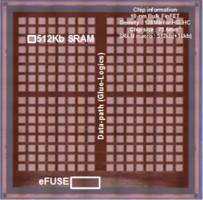
Samsung demonstrated their 128 Megabit SRAM wafer from their 10nm FinFET process. Samsung, which unlike Intel uses LELELE (litho-etch-litho-etch-litho-etch), ramped up mass production in May of 2017. ChipWorks/TechInsight measured the CPP/MMP which came a little short of the Common Platform Alliance Paper which was presented in 2016, at 68 nm contacted gate pitch, 51 nm metal pitch, dual-depth shallow trench isolation (STI), and had single dummy gate.
Samsung's initial process was 10LPE (10 Low-Power Early) which was replaced by second generation evolved process 10LPP (10 Low-Power Plus). Samsung intends to introduce a third generational enhanced 10nm process called 8LPP (8 Low Power Plus) which will further improve performance and introduce a small density increase through cell enhancements and a narrower metal pitch. 8LPP improvements over 10LPP is similar to their 11LPP improvements over their 14LPP. It's worth noting that Samsung intends 8LPP to be their last non-EUV node. All subsequent nodes will use EUV.
| Samsung 128 Mib SRAM demo 10 nm wafer | |||||||||||||||
|---|---|---|---|---|---|---|---|---|---|---|---|---|---|---|---|
|
| ||||||||||||||
TSMC[edit]
TSMC reported a poly pitch of 64 nm with a metal pitch 42 nm. TechInsight measured them at 66 nm and 44 nm respectively. 10FF is the second process to use FinFET, and is the Industry's first use of Quad-Patterning. This allows for a full node shrink, enabling a 2X increase in logic density compared to their 16nm process. The 10FF process will have 15% higher performance while consuming 35% less power.
Specifications[edit]
| Process Name | |
|---|---|
| 1st Production | |
| Litho- graphy |
Lithography |
| Immersion | |
| Exposure | |
| Wafer | Type |
| Size | |
| Tran- sistor |
Type |
| Voltage | |
| Fin | Pitch |
| Width | |
| Height | |
| Gate Length (Lg) | |
| Contacted Gate Pitch (CPP) | |
| Minimum Metal Pitch (MMP) | |
| SRAM bitcell |
High-Perf (HP) |
| High-Density (HD) | |
| Low-Voltage (LV) | |
| DRAM bitcell |
eDRAM |
| Intel | TSMC | Samsung | IBM Paper Common Platform Alliance - The Common Platform Alliance is a joint collaboration between IBM, Samsung, GlobalFoundries, STMicroelectronics, UMC
| ||||
|---|---|---|---|---|---|---|---|
| P1274, P1275 | 10FF | 10LPE 1st generation; 10 nm Low Power Early ,10LPP2nd generation; 10 nm Low Power Plus ,10LPU3rd generation; 10 nm Low Power Ultimate |
|||||
| 2018 | June 2017 | April 2017 | |||||
| 193 nm | 193 nm | 193 nm | 193 nm | ||||
| Yes | Yes | Yes | Yes | ||||
| SAQP | SAQP | LELELE | SADP | ||||
| Bulk | Bulk | Bulk | Bulk/SOI | ||||
| 300 mm | 300 mm | 300 mm | 300 mm | ||||
| FinFET | FinFET | FinFET | FinFET | ||||
| 0.70 V | 0.70 V | 0.75 V | 0.75 V | ||||
| Value | 14 nm Δ | Value | 16 nm Δ | Value | 14 nm Δ | Value | 14 nm Δ |
| 34 nm | 0.81x | 36 nm | 0.75x | 42 nm | 0.88x | ||
| 7 nm | 0.88x | 6 nm | |||||
| 53 nm | 1.26x | 42 nm | 1.35x | ||||
| 20 nm | 1.00x | ||||||
| 54 nm | 0.77x | 66 nm (64 nm*) | 0.73x | 68 nm | 0.87x | 64 nm | 0.80x |
| 36 nm | 0.69x | 44 nm (42 nm*) | 0.69x | 48 nm | 0.75x | 48 nm | 0.75x |
| 0.0441 µm² | 0.62x | 0.049 µm² | 0.61x | ||||
| 0.0312 µm² | 0.62x | 0.042 µm² | 0.57x | 0.040 µm² | 0.63x | 0.053 µm² | 0.65x |
| 0.0367 µm² | 0.62x | ||||||
| . | |||||||
* - Value reported from IEEE ISSCC/IEDM/VLSI Conference.
10 nm process nodes[edit]
| ITRS | Samsung | TSMC | Intel | ||||||||
|---|---|---|---|---|---|---|---|---|---|---|---|
| Process name | 14 nm (16 nm) |
10 nm (11 nm) |
10LPE (10 nm) |
10LPP (10 nm) |
8LPP (8 nm) |
8LPU (8 nm) |
8LPA (8 nm) |
10FF (10 nm) |
P1274/P1275 10 nm (7 nm) |
10 nm SF (7 nm) |
10 nm ESF (Intel 7) |
| Transistor density (MTr/mm2) |
- | - | 51.82 HD | 61.18 HD | - | 52.51 HD [1] | 100.76 HD / 60.41 SHP logic (plus optional 60nm CPP) | ||||
| Transistor gate pitch (nm) |
70 | 48 | 68 | 64 | - | 66 | 54 | ||||
| Interconnect pitch (nm) |
56 | 36 | 51 | - | - | 44 | 36 | ||||
| Transistor fin pitch (nm) |
42 | 36 | 42 | - | 36 | 34 | |||||
| Transistor fin height (nm) |
42 | 42 | 49 | - | - | 42 | 53 | >53 | >53 | ||
| Production year | 2015 release |
2017 release |
2016 Q4 production |
2017 Q4 production |
2018 production |
2018 risk production 2019 production |
2021 production |
2016 risk production 2017 production |
2018 risk production (Cannon Lake) 2019 production (Ice Lake) |
2020 production (Tiger Lake) |
2021 production (Alder Lake) |
10 nm Microprocessors[edit]
This list is incomplete; you can help by expanding it.
10 nm Microarchitectures[edit]
- Intel
- Qualcomm
- Samsung
This list is incomplete; you can help by expanding it.
Documents[edit]
- Intel's 10 nm Technology: Delivering the Highest Logic Transistor Density in the Industry Through the Use of Hyper Scaling
- Intel Technology & Manufacturing Day presentation, 10 nm
- Intel Technology & Manufacturing Day presentation, 10 nm / Moore's Law
References[edit]
- Mark Bohr, Intel. Intel Technology and Manufacturing Day. Mar 28, 2017.
- Samsung uses LELELE based on their press release about their 10nm FinFET Technology on October 17, 2016.
- Seo, K-I., et al. "A 10nm platform technology for low power and high performance application featuring FINFET devices with multi workfunction gate stack on bulk and SOI." VLSI Technology (VLSI-Technology): Digest of Technical Papers, 2014 Symposium on. IEEE, 2014.
- Cho, H-J., et al. "Si FinFET based 10nm technology with multi Vt gate stack for low power and high performance applications." VLSI Technology, 2016 IEEE Symposium on. IEEE, 2016.
- Song, Taejoong, et al. "A 10 nm FinFET 128 Mb SRAM With Assist Adjustment System for Power, Performance, and Area Optimization." IEEE Journal of Solid-State Circuits (2016).
- Clinton, Michael, et al. "12.3 A low-power and high-performance 10nm SRAM architecture for mobile applications." Solid-State Circuits Conference (ISSCC), 2017 IEEE International. IEEE, 2017.
- Samsung's actual transistor size was measured by ChipWorks/TechInsight based on the Qualcomm Snapdragon 835 which is manufactured on Samsung's 10nm process.
- TechInsights TSMC 10 nm Process Analysis
 Semiconductor lithography processes technology
