(Undo revision 66135 by 49.151.20.188 (talk)) |
m (→GlobalFoundries) |
||
| Line 237: | Line 237: | ||
==== GlobalFoundries ==== | ==== GlobalFoundries ==== | ||
| − | Building on top of Samsung's licensed 14nm process, GlobalFoundries announced "12LP" in late 2017 which | + | Building on top of Samsung's licensed 14nm process, GlobalFoundries announced "12LP" in late 2017 which is said to deliver up to 15% increase in density and 10% increase in performance. |
Note that GlobalFoundries "14HP" is just IBM's "14HP". | Note that GlobalFoundries "14HP" is just IBM's "14HP". | ||
Revision as of 14:59, 17 November 2017
The 14 nanometer (14 nm) lithography process is a semiconductor manufacturing process node serving as shrink from the 22 nm process. The term "14 nm" is simply a commercial name for a generation of a certain size and its technology, as opposed to gate length or half pitch. The 14 nm node was introduced in 2014/2015 and is currently getting replaced by the 10 nm process.
Contents
Industry
| Process Name | |
|---|---|
| 1st Production | |
| Litho- graphy |
Lithography |
| Immersion | |
| Exposure | |
| Wafer | Type |
| Size | |
| Tran- sistor |
Type |
| Voltage | |
| Fin | Pitch |
| Width | |
| Height | |
| Gate Length (Lg) | |
| Contacted Gate Pitch (CPP) | |
| Minimum Metal Pitch (MMP) | |
| SRAM bitcell |
High-Perf (HP) |
| High-Density (HD) | |
| Low-Voltage (LV) | |
| DRAM bitcell |
eDRAM |
| Intel | Samsung Alliance Samsung Alliance consists of a process development collaboration between Samsung and GlobalFoundries. GlobalFoundries licenses Samsung's 14nm process at Fab8, New York. |
IBM (Now GlobalFoundries) | UMC | Common Platform Alliance The Common Platform Alliance is a joint collaboration between IBM, STMicroelectronics
| |||||
|---|---|---|---|---|---|---|---|---|---|
| P1272 (CPU) / P1273 (SoC) | 14LPE 1st generation; 14 nm Low Power Early , 14LPP2nd generation; 14 nm Low Power Performance , 14LPC3rd generation; 14 nm Low Power Cost [reduced] , 14LPU4th generation; 14 nm Low Power Ultimate |
14HP 14nm High Performance |
14FDSOI | ||||||
| 2014 | 2015 | 2017 | 2Q 2017 | ||||||
| 193 nm | 193 nm | 193 nm | 193 nm | 193 nm | |||||
| Yes | Yes | Yes | yes | Yes | |||||
| SADP | LELE | SADP | DP | ||||||
| Bulk | Bulk | SOI | bulk | SOI | |||||
| 300 mm | 300 mm | 300 mm | 300 mm | 300 mm | |||||
| FinFET | FinFET | FinFET | FinFET | Planar | |||||
| 0.70 V | 0.80 V | 0.80 V | 0.80 V | ||||||
| Value | 22 nm Δ | Value | 20 nm Δ | Value | 22 nm Δ | Value | 28 nm Δ | Value | 28 nm Δ |
| 42 nm | 0.70x | 48 nm | N/A | 42 nm | N/A | N/A | |||
| 8 nm | 1.00x | 8 nm | 10 nm | ||||||
| 42 nm | 1.24x | ~38 nm | 25 nm | ||||||
| 20 nm | 0.77x | 30 nm | 18-26 nm | 0.72-0.79x | 20 nm | 0.71x | |||
| 70 nm | 0.78x | 78 nm | 1.22x | 80 nm | 0.80x | 90 nm | 0.79x | ||
| 52 nm | 0.65x | 64 nm | 1.00x | 64 nm | 0.80x | 64 nm | 0.71x | ||
| 0.0706 µm² | 0.54x | 0.080 µm² | 0.78x | 0.0900 µm² | 0.63x | 0.090 µm² | 0.59x | ||
| 0.0499 µm² | 0.54x | 0.064 µm² | 0.79x | 0.0810 µm² | 0.81x | 0.081 µm² | 0.68x | ||
| 0.0588 µm² | 0.54x | ||||||||
| 0.0174 µm² | 0.67x | ||||||||
Composition
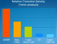
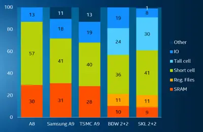
It's important tot note that not all processes compete with each other. The process should cater to the products that will make use of the underlying technology. The composition of the actual integrated circuit also varies by manufacturer and by design due to different goals. For example, the cache on Apple's 14 nm A9 (manufactured by Samsung) accounts almost 1/3 of the entire chip whereas Intel's Broadwell cache accounts for only 10% of the entire chip. Likewise, Intel's Broadwell and Skylake target high-performance and incorporate a large amount of higher-speed elements which are inherently sparse. Tall cells account for almost 30% Skylake's composition and less than 1% on Apple's A8 or A9. Those numbers are somewhat expected given tall logic cells are generally optimized for performance and high frequency (e.g., high-switching circuitry in the CPU) whereas short cells are optimized for density (e.g., GPU shader arrays).
It should be noted that SRAM is the most dense component of the process in a chip, with sometimes up to three or four times the density of logic cells that are used in the same process. It should be noted that in recent years, SRAM hasn't scaled as well as logic and I/O have either.
Intel
- See also: Intel's Process Technology History
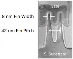
Intel got off to a bumpy start with major yield problems initially, but by Skylake yield has reached very healthy numbers. 14 nm became Intel's 2nd generation FinFET transistors. Intel uses TiN pMOS / TiAlN nMOS as work function metals. Intel makes use of 193 nm immersion lithography with Self-Aligned Double Patterning (SADP) at the critical patterning layers. Compared to all other "14 nm nodes", Intel's process is the densest and considerably so, with >1.5x raw logic density.
Intel's 14 nm process has gone through multiple refinements optimizing higher clock speed, higher drive current, and lower power dissipation. The original "14nm" was used for their Broadwell and mainstream Skylake processors. They improved on their original process with a second process, "14nm+", offering 12% higher drive current at lower power. That process has been used for both Kaby Lake and Server/HEDT Skylake SP/X processors.
A third improved process, "14nm++", is set to begin in late 2017 and will further allow for +23-24% higher drive current for 52% less power vs the original 14nm process. The 14nm++ process also appear to have slightly relaxed poly pitch of 84 nm (from 70 nm). It's unknown what impact, if any, this will have on the density.
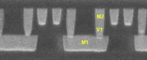
| Intel 14nm Design Rules | ||
|---|---|---|
| Layer | Pitch | Scale Factor |
| Fin | 42 nm | 0.70 |
| Contacted Gate Pitch | 70 nm | 0.78 |
| Metal 0 | 56 | - |
| Metal 1 | 70 | 0.78 |
| Metal 2 | 52 | 0.65 |
IBM
IBM developed their own "14HP" (14nm High-Performance) process at their East Fishkill, NY plant. Note that the plant AND the process, along with numerous semiconductor technology IPs, were sold to GlobalFoundries in late 2014. GF still operates the plant (also by ex-IBM semiconductor engineers) and the process which is used by IBM for their various processors. This process was designed by IBM for their very large chips with effective power supply and clock distribution capable of producing dies as large as 700 mm² and larger with a hierarchical BEOL of 17 levels of copper interconnect for high performance wire-ability. It should be noted that GlobalFoundries had no such capabilities prior to their acquisition of IBM's plant, semiconductor manufacturing group, and IP portfolio.
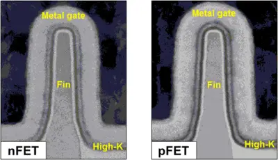
IBM's HP 14nm CMOS process features a FinFET architecture on an SOI substrate. The use of SOI with FinFET gives IBM a number of unique advantages such as lower parasitic capacitance at the base of the fin as well as simplifies patterning of the active fins and minimizes their variability such as height and thickness. The architecture also includes high-density deep-trench embedded DRAM cells with a reported size of 0.0174 µm². The process features an Lgate of 20nm and smaller (18nm to 27nm) which IBM reported to result in over 35% performance gain verses their HP 22nm process (for identical Vdd = 0.80 V).
| IBM 14nm Design Rules | ||
|---|---|---|
| Layer | Pitch | |
| Fin | 42 nm | |
| Contacted Gate Pitch | 80 nm | |
| Metal 1 | 64 nm | |
| Metal 2 | 80 nm | |
| Metal 3 | 128 nm | |
| Metal 4 | 256 nm | |
| Metal 5 | 512 nm | |
| Metal 6 | 2.56 µm | |
Samsung
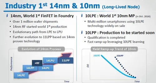
This process became Samsung's and GlobalFoundries first generation of FinFET-based transistors. Samsung uses TiN pMOS / TiAIC nMOS as work function metals. Samsung node has gone through a number of refinements from 14LPE (14 Low-Power Early) to 14LPP (14 Low-Power Performance) and further.
In late 2017, Samsung announced "11LPP" (11 Low-Power Plus) which is a further enhancement of 14LPP. 11LPP is reported to deliver up to 15% higher performance with enhanced design rules that allow for up to 10% reduction in area. Samsung expects 11LPP to enter mass production in late 2017 or early 2018.
GlobalFoundries
Building on top of Samsung's licensed 14nm process, GlobalFoundries announced "12LP" in late 2017 which is said to deliver up to 15% increase in density and 10% increase in performance.
Note that GlobalFoundries "14HP" is just IBM's "14HP".
UMC
UMC announced the start of 14nm process mass production in February 2017. The 14nm process is their first process to use FinFET, and provides up to 55% higher performance and twice the gate density compared to their 28nm process.
Find models
Click to browse all 14 nm MPU models
14 nm Microprocessors
- AMD
- Apple
- Intel
- Samsung
This list is incomplete; you can help by expanding it.
14 nm Microarchitectures
- Intel
- AMD
- IBM
This list is incomplete; you can help by expanding it.
Documents
- Intel's 14 nm Technology: Delivering Ultrafast, Energy-Sipping Products
- Intel's 14nm, Advancing Moore's Law, investor meeting
References
- Natarajan, S., et al. "A 14nm logic technology featuring 2 nd-generation FinFET, air-gapped interconnects, self-aligned double patterning and a 0.0588 µm 2 SRAM cell size." Electron Devices Meeting (IEDM), 2014 IEEE International. IEEE, 2014.
- Lin, C. H., et al. "High performance 14nm SOI FinFET CMOS technology with 0.0174 µm 2 embedded DRAM and 15 levels of Cu metallization." Electron Devices Meeting (IEDM), 2014 IEEE International. IEEE, 2014.
- Jan, C-H., et al. "A 14 nm SoC platform technology featuring 2 nd generation Tri-Gate transistors, 70 nm gate pitch, 52 nm metal pitch, and 0.0499 um 2 SRAM cells, optimized for low power, high performance and high density SoC products." VLSI Technology (VLSI Technology), 2015 Symposium on. IEEE, 2015.
- Song, Taejoong, et al. "A 14 nm FinFET 128 Mb SRAM With VMIN Enhancement Techniques for Low-Power Applications." IEEE Journal of Solid-State Circuits 50.1 (2015): 158-169.
- Weber, Olivier, et al. "14nm FDSOI technology for high speed and energy efficient applications." VLSI Technology (VLSI-Technology): Digest of Technical Papers, 2014 Symposium on. IEEE, 2014.
- Chen, Shyng-Tsong, et al. "64 nm pitch Cu dual-damascene interconnects using pitch split double exposure patterning scheme." Interconnect Technology Conference and 2011 Materials for Advanced Metallization (IITC/MAM), 2011 IEEE International. IEEE, 2011.
 Semiconductor lithography processes technology
