Semiconductor & Computer Engineering
| Edit Values | |
| z14 µarch | |
| General Info | |
| Arch Type | CPU |
| Designer | IBM |
| Manufacturer | GlobalFoundries |
| Introduction | July 17, 2017 |
| Process | 14 nm |
| Core Configs | 7, 8, 9, 10 |
| Pipeline | |
| Type | Superscalar, Pipelined |
| OoOE | Yes |
| Speculative | Yes |
| Reg Renaming | Yes |
| Instructions | |
| ISA | z/Architecture |
| Cache | |
| L1I Cache | 128 KiB |
| L1D Cache | 128 KiB |
| Succession | |
z14 is the successor to z13, a 14 nm z/Architecture mainframe microarchitecture designed by IBM and introduced in 2017.
Contents
Process Technology[edit]
z14-based microprocessors are manufactured on GlobalFoundries's 14 nm (14HP) FinFET Silicon-On-Insulator (SOI) process featuring highly-dense deep trench structures used for high-density eDRAM.
Release Dates[edit]
IBM z14 was announced on July 17, 2017. General availability started on September 13, 2017.
Architecture[edit]

Key changes from z13[edit]
- 14 nm process (from 22 nm)
- 6.1B transistors (from 3.99B; 53% increase)
- Higher clock frequency (5.2 GHz from 5 GHz; 4% increase)
- Higher scalability
- Up to 170-way multiprocessing (from 141-way)
- Core
- Improved Operand Store Compare (OSC) prediction
- Faster branch wakeup
- Improved instruction delivery
- Reduced execution latency
- Cache
- New directory design
- Power efficient
- L1I$ increased to 128 KiB/core (from 96 KiB/core; 33% increase)
- L2D$ increased to 4 MiB/core (from 2 MiB/core; 100% increase)
- L3$ increased to 128 MiB/CP (from 64 MiB/CP; 100% increase)
- New 672 MiB/drawer of shared L4
- New directory design
- TLB
- BTB
- 1.33x larger BTB1
- 1.33x larger BTB2
- New Hashed Perceptron Predictor
- New Simple Call Return Stack
- Central Processor Assist for Cryptographic Function (CPACF)
- Dedicated co-processor for each core
- Claims 6x faster encryption functions (vs. z13)
- 4x Advanced Encryption Standard (AES) speedup
- Support for True Random Number Generator
- New support for SHA-3 standard
This list is incomplete; you can help by expanding it.
New instructions[edit]
Overview[edit]
Mainframe[edit]
The IBM z14 mainframe comes in a number of slightly different flavors. In order to reach the highest clock speed of 5.2 GHz, the water cooled system is required, otherwise the air cooled is sufficient.
.png)
.png)
Each mainframe has two frames that are bolted together. Frames are built to Electronic Industries Alliance (EIA) standards and are 42U EIA frames. Viewed from the front, the right side is called Frame A while the left side is called Frame Z.
Z Frame[edit]
| At the top of the frame is an optional overhead power cabling solution. There are top exit options for fiber optic cables and other ethernet solutions such as FICON, OSA, 12x InfiniBand, 1x InfiniBand, ICA, zHyperLink Express, Coupling Express LR, and RoCE. | |

|
There are two to four optional integrated battery features (IBFs) which serves as a local uninterrupted power source. Additionally, the IBFs provide additional power robustness functionalities such as increases power line disturbance immunity and noise reduction. The number of installed IBFs depends on the number of power regulators that are installed and is always installed in pairs. |

|
A configurable set of Bulk power regulators (BPRs). |

|
The entire bottom part of the rack consists of up to four PCIe I/O drawers, installed top-down. |
A Frame[edit]

|
Two support elements (SE) 1U servers. |

|
One optional PCIe I/O drawer. |
| |
Two System Control Hubs (SCHs). |

|
Up to four CPC drawers with a minimum of at least one must be installed. |

|
Two radiator pumps or two Water Conditioning Units (WCUs) in the case of water cooling. |
System[edit]

The IBM z14 mainframe is the successor to z13, offering a large set of enhancements over the prior generation in all key areas such as scalability, security, and performance.
Drawer[edit]
The IBM z14 mainframe consists of a number of drawers. A drawer is simply a cluster of processors and chipsets. Each drawer consists of two clusters of three central processors (CPs) each and a single system controller (SC) chip. A full drawer can thus have a total of six processors and a single system controller. The X-bus interconnect links each CP chip to every other CP chip in the cluster and each CP chip to the SC chip.

The SC chip can links one drawer to another for up to four drawers in the max z14 mainframe system. In a max configuration, the z14 can have a total of 24 processors. With up to 10 cores per processor, in theory, a maximum-configured system can have a total of 240 cores. Note that some chips are reserved for redundancy, so a max drawer has 41 active cores for a maximum of 164 cores with four drawers. Drawers are linked together by linking each SC to every other SC in the other drawers over the A-bus. This is done through SMP connectors and cables. All four drawers are then fully connected to all other drawers.

Central Processor[edit]
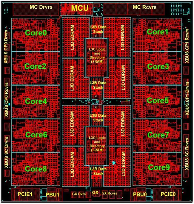
Fabricated on a 14 nm process, the central processor is largely an evolutionary designed based on the previous z13 architecture featuring a very long out-of-order pipeline for high frequency design. Running at up to 5.2 GHz for a 0.192 ns cycle time, chips come with either 7, 8, 9, or 10 active cores enabled.
Die[edit]
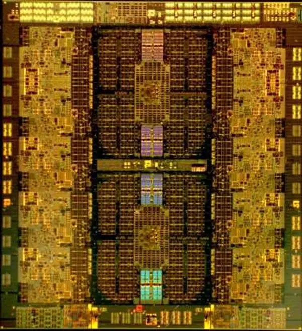
Central Processor (CP) Chip[edit]

- GlobalFoundries 14HP Process
- CMOS FinFET SOI
- 17 Metal Layers
- deca-core (10 Processor Units (PUs))
- 5.2 GHz (192 ps cycle time)
- 6,100,000,000 transistors
- 14.4 miles of copper wire
- 26.5 x 27.8 mm † OR 25.3 mm x 27.5 mm‡ die
- 736.7 mm²† OR 695.75 mm²‡ die size
- 18,581 power pins
- 1,505 signal pins
(† - size provided by IBM in their presentations; ‡ - size provided by the IBM RedBook)
- Floor Plan:
-

- Die:

Core[edit]
Below is a layout of a single physical core:

- L2 - L2I$ + L2D$
- PC + TP - Core pervasive unit (instrumentation/error collection) + Trap
- LSU - Load-store unit (+ L1D$)
- XU - Translation unit (TLB + DAT)
- ICM - Instruction cache & merge
- COP - Dedicated Co-Processor
- FXU - Fixed-point unit
- VFU - Vector and Floating point Unit
- ISU - Instruction sequence unit
- RU - Recovery unit
- IDU - Instruction decode unit
- IFB - Instruction fetch and branch prediction
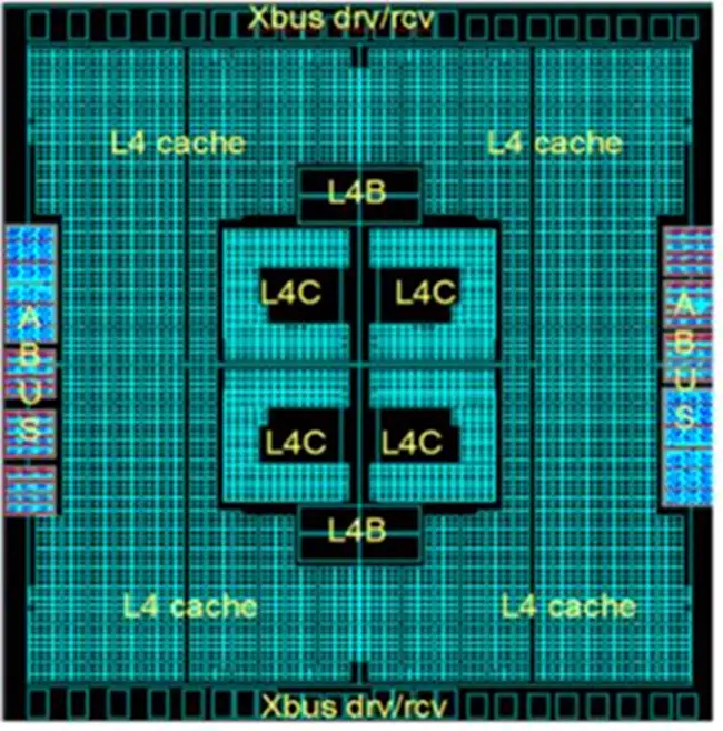
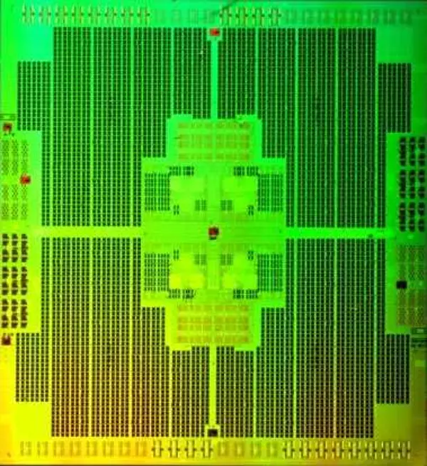
System Controller (SC) Chip[edit]

- GlobalFoundries 14HP Process
- CMOS FinFET SOI
- 17 Metal Layers
- 25.3 x 27.5 mm die
- 695.75 mm² die size
- 7,100,000,000 transistors
- + 2,100,000,000 cells of eDRAM (~2.1B xTors + 2.1B capacitors)
- 672 MiB shared eDRAM L4 Cache
- Floor Plan:
-

- Die:
-

| codename | z14 + |
| core count | 7 +, 8 +, 9 + and 10 + |
| designer | IBM + |
| first launched | July 17, 2017 + |
| full page name | ibm/microarchitectures/z14 + |
| instance of | microarchitecture + |
| instruction set architecture | z/Architecture + |
| manufacturer | GlobalFoundries + |
| microarchitecture type | CPU + |
| name | z14 + |
| process | 14 nm (0.014 μm, 1.4e-5 mm) + |