From WikiChip
Difference between revisions of "16 nm lithography process"
(→Industry) |
(→16 nm Microarchitectures) |
||
| Line 67: | Line 67: | ||
== 16 nm Microarchitectures== | == 16 nm Microarchitectures== | ||
| + | * ARM | ||
| + | ** {{armh|Cortex-A55|l=arch}} | ||
{{expand list}} | {{expand list}} | ||
Revision as of 08:43, 29 May 2017
The 16 nanometer (16 nm) lithography process is a full node semiconductor manufacturing process following the 20 nm process stopgap. Commercial integrated circuit manufacturing using 16 nm process began in 2014. The term "16 nm" is simply a commercial name for a generation of a certain size and its technology, as opposed to gate length or half pitch. This technology is set to be replaced with 10 nm process in 2017.
Industry
An enhanced version of TSMC's 16nm process was introduced in late 2016 called "12nm".
| Process Name | |
|---|---|
| 1st Production | |
| Litho- graphy |
Lithography |
| Immersion | |
| Exposure | |
| Wafer | Type |
| Size | |
| Tran- sistor |
Type |
| Voltage | |
| Fin | Pitch |
| Width | |
| Height | |
| Gate Length (Lg) | |
| Contacted Gate Pitch (CPP) | |
| Minimum Metal Pitch (MMP) | |
| SRAM bitcell |
High-Perf (HP) |
| High-Density (HD) | |
| Low-Voltage (LV) | |
| DRAM bitcell |
eDRAM |
| TSMC | |
|---|---|
| 16FF, 16FF+, 12FFN | |
| 2016 | |
| 193 nm | |
| Yes | |
| Bulk | |
| 300 mm | |
| FinFET | |
| 0.75 V | |
| Value | 20 nm Δ |
| 48 nm | N/A |
| 37 nm | |
| 34 nm | |
| 90 nm | 1x |
| 64 nm | 1x |
| 0.074 µm² | 0.86x |
TSMC
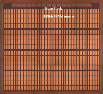
TSMC demonstrated their 128 Mebibit SRAM wafer from their 16 nm HKMG FinFET process at the 2014 IEEE ISSCC.
16 nm Microprocessors
This list is incomplete; you can help by expanding it.
16 nm Microarchitectures
- ARM
This list is incomplete; you can help by expanding it.
References
- Chen, Yen-Huei, et al. "A 16 nm 128 Mb SRAM in High-κ Metal-Gate FinFET Technology With Write-Assist Circuitry for Low-VMIN Applications." IEEE Journal of Solid-State Circuits 50.1 (2015): 170-177.
- Wu, Shien-Yang, et al. "A 16nm FinFET CMOS technology for mobile SoC and computing applications." Electron Devices Meeting (IEDM), 2013 IEEE International. IEEE, 2013.
- TechInsights/Chipworks, Kevin Gibb, The ConFab 2016
 Semiconductor lithography processes technology
