(→TSMC) |
m |
||
| Line 146: | Line 146: | ||
=== Intel === | === Intel === | ||
{{see also|intel/process|l1=Intel's Process Technology History}} | {{see also|intel/process|l1=Intel's Process Technology History}} | ||
| + | [[File:intel 10nm fin.png|right|200px]] | ||
Announced during Intel's Technology and Manufacturing Day 2017, Intel's 10 nm process (P1274) is Intel's frist high-volume manufacturing process to employ [[Self-Aligned Quad Patterning]] (SAQP) with production starting in the second half of 2017. Intel detailed {{intel|Hyper-Scaling}}, a marketing term for a suite of techniques used to [[transistor scaling|scale a transistor]], SAQP, a single dummy gate and [[contact over active gate]] (COAG). Intel's initial 10 nm process has up to 60% lower power and 25% better performance than their initial 14 nm but will actually have lower performance than their "14nm++" process. Intel expect their "10nm+" process to surpass that. | Announced during Intel's Technology and Manufacturing Day 2017, Intel's 10 nm process (P1274) is Intel's frist high-volume manufacturing process to employ [[Self-Aligned Quad Patterning]] (SAQP) with production starting in the second half of 2017. Intel detailed {{intel|Hyper-Scaling}}, a marketing term for a suite of techniques used to [[transistor scaling|scale a transistor]], SAQP, a single dummy gate and [[contact over active gate]] (COAG). Intel's initial 10 nm process has up to 60% lower power and 25% better performance than their initial 14 nm but will actually have lower performance than their "14nm++" process. Intel expect their "10nm+" process to surpass that. | ||
Intel's 10nm process is roughly 1.7x the raw logic density of the next densest 10nm process, albeit due to aggressive pattering techniques they also have the most complex process available to date. | Intel's 10nm process is roughly 1.7x the raw logic density of the next densest 10nm process, albeit due to aggressive pattering techniques they also have the most complex process available to date. | ||
| − | + | {{clear}} | |
| − | |||
=== Samsung === | === Samsung === | ||
| Line 174: | Line 174: | ||
=== TSMC === | === TSMC === | ||
| − | |||
TSMC reported a poly pitch of 64 nm with a metal pitch 42 nm. TechInsight measured them at 66 nm and 44 nm respectively. 10FF is the second process to use FinFET, and is the Industry's first use of Quad-Patterning. This allows for a full node shrink, enabling a 2X increase in logic density compared to their 16nm process. TSMC claims the 10FF process will have 15% higher performance while consuming 35% less power. | TSMC reported a poly pitch of 64 nm with a metal pitch 42 nm. TechInsight measured them at 66 nm and 44 nm respectively. 10FF is the second process to use FinFET, and is the Industry's first use of Quad-Patterning. This allows for a full node shrink, enabling a 2X increase in logic density compared to their 16nm process. TSMC claims the 10FF process will have 15% higher performance while consuming 35% less power. | ||
| + | {{clear}} | ||
| + | [[File:10nm tsmc.jpeg|200px]] | ||
== 10 nm Microprocessors== | == 10 nm Microprocessors== | ||
Revision as of 15:47, 12 August 2017
The 10 nanometer (10 nm) lithography process is a semiconductor manufacturing process node serving as shrink from the 14 nm process. The term "10 nm" is simply a commercial name for a generation of a certain size and its technology, as opposed to gate length or half pitch. The 10 nm node is currently being introduced and is set to get replaced by the 7 nm process in 2019.
Contents
Industry
At the advanced 10nm process, there are only 3 semiconductor foundries with such manufacturing capabilities: Intel, Samsung, and TSMC.
Due to marketing names, geometries vary greatly between leading manufactures. Although both TSMC and Samsung's 10nm processes are slightly denser than Intel's 14nm in raw logic density, they are far closer to Intel's 14nm than they are to Intel's 10nm (e.g., Samsung's metal pitch just 1 nanometer shorter than Intel's 14nm).
| Process Name | |
|---|---|
| 1st Production | |
| Lithography | Lithography |
| Immersion | |
| Exposure | |
| Wafer | Type |
| Size | |
| Transistor | Type |
| Voltage | |
| Fin | Pitch |
| Width | |
| Height | |
| Gate Length (Lg) | |
| Contacted Gate Pitch (CPP) | |
| Minimum Metal Pitch (MMP) | |
| SRAM bitcell | High-Perf (HP) |
| High-Density (HD) | |
| Low-Voltage (LV) | |
| DRAM bitcell | eDRAM |
| Intel | TSMC | Samsung | Common Platform Alliance The Common Platform Alliance is a joint collaboration between IBM, Samsung, GlobalFoundries, STMicroelectronics, UMC Paper
| ||||
|---|---|---|---|---|---|---|---|
| P1274 (CPU) / P1275 (SoC) | 10FF | 10LPE 1st generation; 10 nm Low Power Early , 10LPP2nd generation; 10 nm Low Power Performance , 10LPU3rd generation; 10 nm Low Power Ultimate |
|||||
| 2017 | June 2017 | April 2017 | |||||
| 193 nm | 193 nm | 193 nm | 193 nm | ||||
| Yes | Yes | Yes | Yes | ||||
| SAQP | SAQP | LELELE | SADP | ||||
| Bulk | Bulk | Bulk | Bulk/SOI | ||||
| 300 mm | 300 mm | 300 mm | 300 mm | ||||
| FinFET | FinFET | FinFET | FinFET | ||||
| 0.70 V | 0.70 V | 0.75 V | 0.75 V | ||||
| Value | 14 nm Δ | Value | 16 nm Δ | Value | 14 nm Δ | Value | 14 nm Δ |
| 34 nm | 0.81x | ||||||
| 53 nm | 1.26x | ||||||
| 20 nm | 1.00x; | ||||||
| 54 nm | 0.77x | 66 nm (64 nm*) | 0.73x | 68 nm | 0.87x | 64 nm | 0.80x |
| 36 nm | 0.69x | 44 nm (42 nm*) | 0.69x | 51 nm | 0.80x | 48 nm | 0.75x |
| 0.0441 µm² | 0.62x | 0.049 µm² | 0.61x | ||||
| 0.0312 µm² | 0.62x | 0.042 µm² | 0.57x | 0.040 µm² | 0.63x | 0.053 µm² | 0.65x |
| 0.0367 µm² | 0.62x | ||||||
* - Value reported from IEEE ISSCC/IEDM/VLSI Conference.
Intel
- See also: Intel's Process Technology History
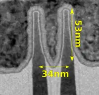
Announced during Intel's Technology and Manufacturing Day 2017, Intel's 10 nm process (P1274) is Intel's frist high-volume manufacturing process to employ Self-Aligned Quad Patterning (SAQP) with production starting in the second half of 2017. Intel detailed Hyper-Scaling, a marketing term for a suite of techniques used to scale a transistor, SAQP, a single dummy gate and contact over active gate (COAG). Intel's initial 10 nm process has up to 60% lower power and 25% better performance than their initial 14 nm but will actually have lower performance than their "14nm++" process. Intel expect their "10nm+" process to surpass that.
Intel's 10nm process is roughly 1.7x the raw logic density of the next densest 10nm process, albeit due to aggressive pattering techniques they also have the most complex process available to date.
Samsung
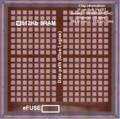
Samsung demonstrated their 128 Mebibit SRAM wafer from their 10nm FinFET process. Samsung, which unlike Intel uses LELELE (litho-etch-litho-etch-litho-etch), ramped up mass production in May of 2017. ChipWorks/TechInsight measured the CPP/MMP which came a little short of the Common Platform Alliance Paper which was presented in 2016, at 68 mm contacted gate pitch, 51 nm metal pitch, dual-depth shallow trench isolation (STI), and had single dummy gate.
| Samsung 128 Mib SRAM demo 10 nm wafer | |||||||||||||||
|---|---|---|---|---|---|---|---|---|---|---|---|---|---|---|---|
|

| ||||||||||||||
TSMC
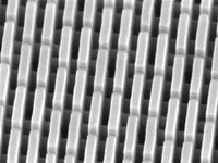
TSMC reported a poly pitch of 64 nm with a metal pitch 42 nm. TechInsight measured them at 66 nm and 44 nm respectively. 10FF is the second process to use FinFET, and is the Industry's first use of Quad-Patterning. This allows for a full node shrink, enabling a 2X increase in logic density compared to their 16nm process. TSMC claims the 10FF process will have 15% higher performance while consuming 35% less power.
10 nm Microprocessors
- Apple
- MediaTek
- Qualcomm
- Xiaomi
This list is incomplete; you can help by expanding it.
10 nm Microarchitectures
- Intel
- Qualcomm
This list is incomplete; you can help by expanding it.
Documents
- Intel's 10 nm Technology: Delivering the Highest Logic Transistor Density in the Industry Through the Use of Hyper Scaling
- Intel Technoogy & Manufacturing Day presentation, 10 nm
- Intel Technoogy & Manufacturing Day presentation, 10 nm / Moore's Law
References
- Mark Bohr, Intel. Intel Technology and Manufacturing Day. Mar 28, 2017.
- Samsung uses LELELE based on their press release about their 10nm FinFET Technology on October 17, 2016.
- Seo, K-I., et al. "A 10nm platform technology for low power and high performance application featuring FINFET devices with multi workfunction gate stack on bulk and SOI." VLSI Technology (VLSI-Technology): Digest of Technical Papers, 2014 Symposium on. IEEE, 2014.
- Cho, H-J., et al. "Si FinFET based 10nm technology with multi Vt gate stack for low power and high performance applications." VLSI Technology, 2016 IEEE Symposium on. IEEE, 2016.
- Song, Taejoong, et al. "A 10 nm FinFET 128 Mb SRAM With Assist Adjustment System for Power, Performance, and Area Optimization." IEEE Journal of Solid-State Circuits (2016).
- Clinton, Michael, et al. "12.3 A low-power and high-performance 10nm SRAM architecture for mobile applications." Solid-State Circuits Conference (ISSCC), 2017 IEEE International. IEEE, 2017.
- Samsung's actual transitor size was measured by ChipWorks/TechInsight based on the Qualcomm Snapdragon 835 which is manufactured on Samsung's 10nm process.
- TechInsights TSMC 10 nm Process Analysis
 Semiconductor lithography processes technology

