(some more minor changes) |
(→Industry) |
||
| (65 intermediate revisions by 31 users not shown) | |||
| Line 1: | Line 1: | ||
{{lithography processes}} | {{lithography processes}} | ||
| − | The '''7 nanometer (7 nm) lithography process''' is a [[technology node]] semiconductor manufacturing process following the [[10 nm lithography process|10 nm process]] node. | + | The '''7 nanometer (7 nm) lithography process''' is a [[technology node]] semiconductor manufacturing process following the [[10 nm lithography process|10 nm process]] node. Mass production of [[integrated circuit]] fabricated using a 7 nm process began in 2018. The process technology will be phased out by leading-edge foundries by 2020/21 timeframe where it will be replaced by the [[5 nm node]]. |
| − | == | + | The term "7 nm" is simply a commercial name for a generation of a certain size and its technology, and '''does not''' represent any geometry of the transistor. |
| − | + | ||
| + | == Overview == | ||
| + | First introduced by the major foundries around the [[2018]]-19 timeframe, the 7-nanometer [[process technology]] is characterized by its use of [[FinFET]] transistors with fin pitches in the 30s of nanometer and densest metal pitches in the upper 30s or low 50s of nanometers. Due to the small feature sizes, [[quad patterning]] had to be utilized for some layers. This process was introduced just as [[EUV Lithography]] became ready for mass production, therefore some foundries utilized EUV while others didn't. | ||
| + | |||
| + | === Density === | ||
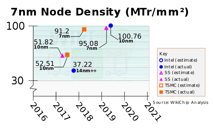
| + | In terms of raw cell-level density, the 7-nanometer node features silicon densities between 90-102 million [[transistors per square millimeter]] based on WikiChip's own analysis. | ||
| − | + | :[[File:7nm densities.svg|700px]] | |
| + | == Industry == | ||
| + | now four companies are currently planning or developing a 7-nanometer node: [[Intel]], [[TSMC]], [[Samsung]] and [[SMIC]]. | ||
| − | {{ | + | {{node comp|node=7 nm}} |
| − | |||
| − | |||
| − | |||
| − | |||
| − | |||
| − | |||
| − | |||
| − | |||
| − | |||
| − | |||
| − | |||
| − | |||
| − | |||
| − | |||
| − | |||
| − | |||
| − | |||
| − | |||
| − | |||
| − | |||
| − | |||
| − | |||
| − | |||
| − | |||
| − | |||
| − | |||
| − | |||
| − | |||
| − | |||
| − | |||
| − | |||
| − | |||
| − | |||
| − | |||
| − | |||
| − | |||
| − | |||
| − | |||
| − | |||
| − | |||
| − | |||
| − | |||
| − | |||
| − | |||
| − | |||
| − | |||
| − | |||
| − | |||
| − | |||
| − | |||
| − | |||
| − | |||
| − | |||
| − | |||
| − | |||
| − | |||
| − | |||
| − | |||
| − | |||
| − | |||
| − | |||
| − | |||
| − | |||
| − | |||
| − | |||
| − | |||
| − | |||
| − | |||
| − | |||
| − | |||
| − | |||
| − | |||
| − | |||
| − | |||
| − | |||
| − | |||
| − | |||
| − | |||
| − | |||
| − | |||
| − | |||
| − | |||
| − | |||
| − | |||
| − | |||
| − | |||
| − | |||
| − | |||
| − | |||
| − | |||
| − | |||
| − | |||
| − | |||
| − | |||
| − | |||
| − | |||
| − | |||
| − | |||
| − | |||
| − | |||
| − | |||
| − | |||
| − | |||
| − | |||
| − | |||
| − | |||
| − | |||
| − | |||
| − | |||
| − | |||
| − | |||
| − | |||
| − | |||
| − | |||
| − | |||
| − | |||
| − | |||
| − | |||
| − | |||
| − | |||
| − | |||
| − | |||
| − | |||
| − | |||
| − | |||
| − | |||
| − | |||
| − | |||
| − | |||
| − | |||
| − | |||
| − | |||
| − | |||
| − | |||
| − | |||
| − | |||
| − | |||
| − | |||
| − | |||
| − | |||
| − | |||
| − | |||
| − | |||
| − | |||
| − | |||
| − | |||
| − | |||
| − | |||
| − | |||
| − | |||
| − | |||
| − | |||
| − | |||
| − | |||
| − | |||
| − | |||
| − | |||
| − | |||
| − | |||
| − | |||
| − | }} | ||
=== Intel === | === Intel === | ||
| − | + | ==== Intel 7 ==== | |
| − | + | ===== Intel 7 Ultra ===== | |
| − | + | [[File:raptor-lake-v-f-curve-improvements.png|thumb|right|New V-F Curve for the Enhanced Intel 7 process.]] | |
| + | Intel introduced an '''enhanced version of the Intel 7 process''' in late 2022 with the introduction of the company's 13th Generation Core processors based on the {{intel|Raptor Lake|l=arch}} microarchitecture. Nicknamed '''"Intel 7 Ultra"''' internally, the new process is a full PDK update over the one used by Alder Lake, their 3rd generation SuperFin Transistor architecture. Intel says this process brings transistors with significantly better channel mobility. At the very high end of the V-F curve, the company says peak frequency is nearly 1 GHz higher now. The curve itself has been improved, shifting prior-generation frequencies by around 200 MHz at ISO-voltage, or alternatively, reducing the voltage by over 50 mV at ISO-frequency. | ||
| − | === | + | === TSMC === |
| − | + | TSMC started mass production of its '''7-nanometer N7 node''' in April 2018. TSMC considers its 7-nanometer node a full node shrink over its 16-nanometer. Although TSMC has released a 10-nanometer node the year prior, the company considered its 10 nm to be a short-lived node and was intended to serve as a learning node on its way to 7. In early 2019 TSMC introduced the second version of its N7 process called '''N7P''' which provides additional performance enhancements. With the availability of [[asml/nxe|high-throughput EUV machines]] ready for mass production, TSMC introduced a third variant called '''N7+''' which uses EUV. | |
| − | |||
| − | |||
| − | + | ==== N7 ==== | |
| + | [[File:n7_overview_slide.jpg|right|thumb|N7 Overview]] | ||
| + | TSMC original '''7-nanometer N7 process''' was introduced in April 2018. Compared to its own [[16-nanometer technology]], TSMC claims its 7 nm node provides around 35-40% speed improvement or 65% lower power. Compared to the half-node [[N10|10 nm node]], N7 is said to provide ~20% speed improvement or ~40% power reduction. In terms of density, N7 is said to deliver 1.6x and 3.3x improvement compared to [[N10]] and [[N16]] respectively. N7 largely builds on all prior FinFET processes the company has had previously. To that end, this is a fourth-generation [[FinFET]], fifth-generation [[HKMG]], gate-last, dual gate oxide process. | ||
| − | === | + | {| class="wikitable" style="text-align: center;" |
| − | [[ | + | |- |
| − | + | ! colspan="3" | N7 [[PPA]] vs. [[N16]] | |
| + | |- | ||
| + | ! Speed @ iso-power !! Power @ iso-speed !! Density | ||
| + | |- | ||
| + | | ~30% || ~55% || ~3.3x | ||
| + | |- | ||
| + | ! colspan="3" | N7 PPA vs. [[N10]] | ||
| + | |- | ||
| + | ! Speed @ iso-power !! Power @ iso-speed !! Density | ||
| + | |- | ||
| + | | ~20% || ~40% || ~1.6x | ||
| + | |} | ||
| − | + | [[File:tsmc-weff-16-10-7.svg|thumb|right|W<sub>eff</sub> for TSMC [[N16|16]], [[N10|10]], and 7 nm.]] | |
| − | TSMC | + | For N7, TSMC continued to use [[deep ultraviolet]] (DUV) 193 nm ArF Immersion lithography. The limitations of i193 dictated some of the design rules for the process. For the transistor, the gate pitch has been further scaled down to 57 nm, however, the interconnect pitch halted at the 40 nm point in order to keep patterning at the [[SADP]] point. Design rules were carefully made to stay within double patterning. Single patterning was pushed slightly further to the 76 nanometers point. The design rules for N7 are shown below. |
| − | {| class=" | + | {| class="wikitable" style="text-align: center;" |
| + | ! colspan="4" | TSMC N7 Design Rules | ||
| + | |- | ||
| + | ! Layer !! Pitch (nm) !! Patterning !! Notes | ||
| + | |- | ||
| + | | Fin || 30 || SAQP || | ||
| + | |- | ||
| + | | Poly || 57 || SADP || | ||
| + | |- | ||
| + | | M0 || 40 || SADP || Mx | ||
| + | |- | ||
| + | | M1 || 40 || SADP || 1x | ||
| + | |- | ||
| + | | M2 || 40 || SADP || 1x | ||
| + | |- | ||
| + | | M3 || 40 || SADP || 1x | ||
| + | |- | ||
| + | | M4 || 40 || SADP || 1x | ||
| + | |- | ||
| + | | M5 || 76 || Single || 1.9x | ||
| + | |- | ||
| + | | M6 || 76 || Single || 1.9x | ||
| + | |- | ||
| + | | M7 || 76 || Single || 1.9x | ||
| + | |- | ||
| + | | M8 || 76 || Single || 1.9x | ||
| + | |- | ||
| + | | M9 || 76 || Single || 1.9x | ||
|- | |- | ||
| − | + | | M10 || 124 || Single || 3.1x | |
|- | |- | ||
| − | | | + | | M11, M12 || 720 || Single || 18x |
| − | <table class="wikitable"> | + | |} |
| − | <tr><th> | + | |
| − | <tr><th> | + | It's worth pointing out that the aggressive [[fin pitch]] scaling have resulted in a fairly dense [[SRAM bitcells]]. The N7 high-density [[SRAM bitcell]] is 0.027 µm². |
| − | <tr><th> | + | |
| − | <tr><th> | + | [[File:mss-n7-a12.jpg|right|thumb|Elements distribution of Apple's A12 SoC (MSS Corp). Cobalt contacts can be seen.]] |
| − | <tr><th> | + | The transistor profile has been enhanced as well. Like [[Intel's 10 nm process]], TSMC introduced cobalt fill at the [[trench contacts]], replacing the tungsten contact. This has the effect of reducing the resistance in that area by 50%. Some of the area scaling and cost benefits were achieved through [[fin pitch]]/[[fin height|height]] [[scaling]]. Continuing to scale the fin width gives you a narrower channel while increasing the height to maintain a good effective width is done in order to improve the short channel characteristics and [[subthreshold slope]] (i.e., improved Ieff / Ceff) but it also degrades the overall parasitics. Keep in mind that overall, the CV/I [[device delay]] is still better because the [[intrinsic capacitance]] like the [[Cgate]] and [[Cov]] still scale with [[Ieff]]. |
| − | <tr><th> | + | |
| − | < | + | Another way to visualize the effect of the width and height scaling is through the effective width. In the graph shown on the left, we plotted the effective width from TSMC 16 nanometer to the current 7-nanometer node. Compared to [[N16]], N7 has over twice the effective channel width. |
| − | <tr><th> | + | |
| + | Different multi-Vt devices were developed for this process with a Vt range of around 200 mV. | ||
| + | |||
| + | ===== Std Cells ===== | ||
| + | TSMC 7-nanometer (N7 and N7P are the same with this regard) comes in two variations - high density and high performance. Those [[standard cell|cells]] are 240 nm and 300 nm tall respectively. Prior to full production ramp, TSMC originally had a 9T HP variant that relied on a 57-nm CPP. That library was eventually obsoleted in favor of a 64-nm CPP 7.5T library which is now used in mass production by various companies. Note that the 7.5T and 9T are similar in power and performance. Some early designs that started out with a 9T library continued to use it regardless. | ||
| + | |||
| + | <table class="wikitable" style="text-align: center;"> | ||
| + | <tr><th>Type</th><th>High Density</th><th colspan="2">High Performance</th></tr> | ||
| + | <tr><th>Name</th><td>H240 HD</td><td>H300 HP</td><td style="text-decoration:line-through">H360 HP</td></tr> | ||
| + | <tr><th>Fin Pitch</th><td colspan="3">30 nm</td></tr> | ||
| + | <tr><th>Metal</th><td colspan="3">40 nm (smallest pitch used with DP)<br>76 nm (smallest pitch used with SP)</td></tr> | ||
| + | <tr><th>Gate Pitch</th><td>57 nm</td><td>64 nm</td><td style="text-decoration:line-through">57 nm</td></tr> | ||
| + | <tr><th>Height</th><td>240 nm<br>8-fin x 30 nm</td><td>300 nm<br>10-fin x 30 nm</td><td style="text-decoration:line-through">360 nm<br>12-fin x 30 nm</td></tr> | ||
| + | <tr><th>Tracks</th><td>6 T</td><td>7.5 T</td><td style="text-decoration:line-through">9 T</td></tr> | ||
</table> | </table> | ||
| − | | [[File: | + | |
| + | [[File:n7_cell_height.svg|500px]] | ||
| + | [[File:sdm855-n7-hd-hp-ieff.png|thumb|right|Qualcomm's [[Snapdragon 855]] [[Ieff]] difference between the HD and HP cells. (VLSI 2019)]] | ||
| + | Qualcomm reported that on its own SoC ([[Snapdragon 855]]), the high-performance cells deliver around 10-13% higher effective drive current ([[Ieff]]), albeit at the cost of being slightly leakier transistors. Based on WikiChip's own analysis, the dense cells come at around 91.2 [[MTr/mm²]] while the less dense, high-performance cells, are calculated at around 65 MTr/mm². | ||
| + | |||
| + | {{clear}} | ||
| + | |||
| + | ==== N7P ==== | ||
| + | [[File:vlsi-2019-n7p-2nd-gen-perf.png|200px|thumb|right|N7P (2nd Gen) vs N7 (1st Gen) improvements. (VLSI 2019)]] | ||
| + | In 2019 TSMC introduced a 2nd-generation N7 process called '''N7 Performance-enhanced''' ('''N7P'''). N7P is an optimized version of TSMC [[#N7|N7]] process. to that end, it remains a [[DUV]]-based process, keeping the same design rules and is fully IP-compatible with N7. N7P introduces [[FEOL]] and [[MOL]] optimizations which are said to translate to either 7% performance improvement at iso-power or up to 10% lower power at iso-speed. | ||
| + | |||
| + | {| class="wikitable" style="text-align: center;" | ||
| + | |- | ||
| + | ! colspan="3" | N7 [[PPA]] vs. N7P | ||
| + | |- | ||
| + | ! Speed @ iso-power !! Power @ iso-speed | ||
| + | |- | ||
| + | | ~7% || ~10% | ||
|} | |} | ||
| − | === Samsung=== | + | For their second generation process, TSMC made some additional optimizations, including fin profile optimizations, [[epitaxial|epi]] optimizations, MOL resistance optimizations, FEOL capacitance reduction, and metal gate optimizations. Additionally, at the same leakage, at high frequencies, the second-generation 7nm process has improved the Vmin by 50 mV. |
| + | |||
| + | {{clear}} | ||
| + | |||
| + | ==== N7+ ==== | ||
| + | The '''N7+ node''' is TSMC's first process technology to adopt [[EUV lithography]]. It is unrelated to both the N7 and N7P processes, and is not IP-compatible with either, requiring re-implementation (new physical layout and validation). N7+ entered mass production in the second quarter of 2019 and uses EUV for four critical layers. Compared to TSMC N7 process, N7+ is said to deliver around 1.2x density improvement. N7+ is also said to deliver 10% higher performance at iso-power or, alternatively, up to 15% lower power at iso-performance. On paper, N7+ appears to be marginally better than N7P, albeit that comes at the cost of re-implementing the design. | ||
| + | |||
| + | {| class="wikitable" style="text-align: center;" | ||
| + | |- | ||
| + | ! colspan="3" | N7 [[PPA]] vs. N7+ | ||
| + | |- | ||
| + | ! Speed @ iso-power !! Power @ iso-speed !! Density | ||
| + | |- | ||
| + | | ~10% || ~15% || 1.2x | ||
| + | |} | ||
| + | |||
| + | {{clear}} | ||
| + | |||
| + | === Samsung === | ||
Samsung will use EUVL for their 7nm node and thus will be the first to introduce this new technology after more than a decade of development. | Samsung will use EUVL for their 7nm node and thus will be the first to introduce this new technology after more than a decade of development. | ||
On May 24 2017, Samsung released a press release of their updated roadmap. Due to delays in the introduction of EUVL, Samsung will introduce a new process called 8nm LPP, to bridge the gap between 10nm and 7nm. The process will be manufactured without the use of EUVL and will feature a slightly relaxed transistor size. | On May 24 2017, Samsung released a press release of their updated roadmap. Due to delays in the introduction of EUVL, Samsung will introduce a new process called 8nm LPP, to bridge the gap between 10nm and 7nm. The process will be manufactured without the use of EUVL and will feature a slightly relaxed transistor size. | ||
| + | ==== 7LPE ==== | ||
| + | ==== 7LPP ==== | ||
| + | === GlobalFoundries === | ||
| + | |||
| + | * '''Note:''' As of august 2018 GlobalFoundries has announced they will suspend further development of their 7nm, 5nm and 3nm process. | ||
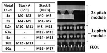
| + | [[File:globalfoundries interconnect 7nm.jpg|right|350px]] | ||
| + | On May 30 2017, GlobalFoundries Senior Vice President and head of CMOS Business Unit, Gregg Bartlett, announced their updated roadmap. Instead of [[EUV]], the company will use multiple patterning 193i for their 7 nm node. The company is planning on first tape-out in the 2nd half of 2018 with mass production to begin in 2019. Bartlett noted that GF will switch to EUVL when it's ready. | ||
| + | |||
| + | The 7nm process features SAQP for the FEOL, and double patterning for the BEOL. GlobalFoundries claims a 2.8 times density improvement compared to their 14nm process, and a performance improvement of 40% or a 55% reduction in power consumption. Two versions of the process will be developed: a low power version for mobile applications. And a high performance version for desktop and server chips. | ||
| + | ==== 7LP ==== | ||
| + | ==== 7HPC ==== | ||
== 7 nm Microprocessors== | == 7 nm Microprocessors== | ||
| Line 216: | Line 160: | ||
** {{pezy|PEZY-SC3}} | ** {{pezy|PEZY-SC3}} | ||
* MediaTek | * MediaTek | ||
| − | ** {{mediatek|Helio M70}} | + | ** {{mediatek|helio|Helio M70}} |
| + | **DImensity 1000 | ||
| + | **Dimensity 800U | ||
| + | **Dimensity 1000+ | ||
| + | **Dimensity 800 | ||
* Apple | * Apple | ||
** {{apple|A12}} | ** {{apple|A12}} | ||
| + | ** {{apple|A12X}} | ||
| + | ** {{apple|A13}} | ||
* HiSilicon (Huawei) | * HiSilicon (Huawei) | ||
| − | ** {{ | + | ** {{hisilicon|kirin|990 4G/5G}} |
| − | * Qualcomm | + | ** {{hisilicon|kirin|980}} |
| − | ** {{Snapdragon | + | ** {{hisilicon|kirin|810}} |
| + | * Snapdragon (Qualcomm) | ||
| + | **Snapdragon 765G | ||
| + | ** {{qualcomm|snapdragon 855|855}} | ||
| + | ** {{qualcomm|snapdragon 865|865}} | ||
| + | ** {{qualcomm|snapdragon 870|870}} | ||
| + | ** {{qualcomm|Snapdragon 865+}} | ||
| + | * Exynos (Samsung) | ||
| + | ** {{samsung|exynos 990|990}} | ||
| + | ** {{samsung|exynos 9825|9825}} | ||
{{expand list}} | {{expand list}} | ||
== 7 nm Microarchitectures== | == 7 nm Microarchitectures== | ||
* AMD | * AMD | ||
| + | ** {{amd|Vega 20|l=arch}} | ||
** {{amd|Navi|l=arch}} | ** {{amd|Navi|l=arch}} | ||
** {{amd|Zen 2|l=arch}} | ** {{amd|Zen 2|l=arch}} | ||
| Line 241: | Line 201: | ||
== See also == | == See also == | ||
| + | * {{intel|process|Intel process technology history}} | ||
| − | * {{ | + | == Bibliography == |
| − | + | * {{bib|iitc|2016|IBM, GlobalFoundries}} | |
| − | + | * {{bib|iedm|2016|Samsung}} | |
| − | * | + | * {{bib|isscc|2017|TSMC}} |
| − | * | + | * {{bib|vlsi|2019|Qualcomm, TSMC}} |
| − | |||
| − | |||
Latest revision as of 01:40, 5 November 2022
The 7 nanometer (7 nm) lithography process is a technology node semiconductor manufacturing process following the 10 nm process node. Mass production of integrated circuit fabricated using a 7 nm process began in 2018. The process technology will be phased out by leading-edge foundries by 2020/21 timeframe where it will be replaced by the 5 nm node.
The term "7 nm" is simply a commercial name for a generation of a certain size and its technology, and does not represent any geometry of the transistor.
Contents
Overview[edit]
First introduced by the major foundries around the 2018-19 timeframe, the 7-nanometer process technology is characterized by its use of FinFET transistors with fin pitches in the 30s of nanometer and densest metal pitches in the upper 30s or low 50s of nanometers. Due to the small feature sizes, quad patterning had to be utilized for some layers. This process was introduced just as EUV Lithography became ready for mass production, therefore some foundries utilized EUV while others didn't.
Density[edit]
In terms of raw cell-level density, the 7-nanometer node features silicon densities between 90-102 million transistors per square millimeter based on WikiChip's own analysis.
Industry[edit]
now four companies are currently planning or developing a 7-nanometer node: Intel, TSMC, Samsung and SMIC.
| Intel | TSMC | Samsung | GlobalFoundries | ||||||
|---|---|---|---|---|---|---|---|---|---|
| Process | P1276 (CPU), P1277 (SoC) | N7, N7P, N7+ | 7LPE, 7LPP | ||||||
| Production | 2021 | April 2018 | April 2019 | Cancelled | |||||
| Litho | Lithography | EUV | DUV ⇒ EUV | EUV | DUV ⇒ EUV | ||||
| Immersion Exposure | SADP ⇒ SE (EUV) DP (193i) | SE (EUV) DP (193i) | SADP ⇒ SE (EUV) DP (193i) | ||||||
| Wafer | Type | Bulk | |||||||
| Size | 300 mm | ||||||||
| xTor | Type | FinFET | |||||||
| Voltage | |||||||||
| Value | 10 nm Δ | Value | 10 nm Δ | Value | 10 nm Δ | Value | 14 nm Δ | ||
| Fin | Pitch | 30 nm | 0.83x | 27 nm | 0.64x | 30 nm | 0.625x | ||
| Width | 6 nm | 1.00x | |||||||
| Height | 52 nm | 1.24x | |||||||
| Gate Length (Lg) | 8/10 nm | ||||||||
| Contacted Gate Pitch (CPP) | 64 nm (HP) 57 nm (HD) | 0.82x | 60 nm (HP) 54 nm (HD) | 0.79x | 56 nm | 0.72x | |||
| Minimum Metal Pitch (MMP) | 40 nm | 0.95x | 36 nm | 0.75x | 40 nm | 0.625x | |||
| SRAM | High-Perf (HP) | 0.032 µm² | 0.65x | 0.0353 µm² | 0.44x | ||||
| High-Density (HD) | 0.027 µm² | 0.64x | 0.026 µm² | 0.65x | 0.0269 µm² | 0.42x | |||
| Low-Voltage (LV) | |||||||||
Intel[edit]
Intel 7[edit]
Intel 7 Ultra[edit]
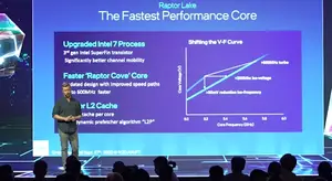
Intel introduced an enhanced version of the Intel 7 process in late 2022 with the introduction of the company's 13th Generation Core processors based on the Raptor Lake microarchitecture. Nicknamed "Intel 7 Ultra" internally, the new process is a full PDK update over the one used by Alder Lake, their 3rd generation SuperFin Transistor architecture. Intel says this process brings transistors with significantly better channel mobility. At the very high end of the V-F curve, the company says peak frequency is nearly 1 GHz higher now. The curve itself has been improved, shifting prior-generation frequencies by around 200 MHz at ISO-voltage, or alternatively, reducing the voltage by over 50 mV at ISO-frequency.
TSMC[edit]
TSMC started mass production of its 7-nanometer N7 node in April 2018. TSMC considers its 7-nanometer node a full node shrink over its 16-nanometer. Although TSMC has released a 10-nanometer node the year prior, the company considered its 10 nm to be a short-lived node and was intended to serve as a learning node on its way to 7. In early 2019 TSMC introduced the second version of its N7 process called N7P which provides additional performance enhancements. With the availability of high-throughput EUV machines ready for mass production, TSMC introduced a third variant called N7+ which uses EUV.
N7[edit]
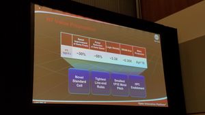
TSMC original 7-nanometer N7 process was introduced in April 2018. Compared to its own 16-nanometer technology, TSMC claims its 7 nm node provides around 35-40% speed improvement or 65% lower power. Compared to the half-node 10 nm node, N7 is said to provide ~20% speed improvement or ~40% power reduction. In terms of density, N7 is said to deliver 1.6x and 3.3x improvement compared to N10 and N16 respectively. N7 largely builds on all prior FinFET processes the company has had previously. To that end, this is a fourth-generation FinFET, fifth-generation HKMG, gate-last, dual gate oxide process.
| N7 PPA vs. N16 | ||
|---|---|---|
| Speed @ iso-power | Power @ iso-speed | Density |
| ~30% | ~55% | ~3.3x |
| N7 PPA vs. N10 | ||
| Speed @ iso-power | Power @ iso-speed | Density |
| ~20% | ~40% | ~1.6x |
For N7, TSMC continued to use deep ultraviolet (DUV) 193 nm ArF Immersion lithography. The limitations of i193 dictated some of the design rules for the process. For the transistor, the gate pitch has been further scaled down to 57 nm, however, the interconnect pitch halted at the 40 nm point in order to keep patterning at the SADP point. Design rules were carefully made to stay within double patterning. Single patterning was pushed slightly further to the 76 nanometers point. The design rules for N7 are shown below.
| TSMC N7 Design Rules | |||
|---|---|---|---|
| Layer | Pitch (nm) | Patterning | Notes |
| Fin | 30 | SAQP | |
| Poly | 57 | SADP | |
| M0 | 40 | SADP | Mx |
| M1 | 40 | SADP | 1x |
| M2 | 40 | SADP | 1x |
| M3 | 40 | SADP | 1x |
| M4 | 40 | SADP | 1x |
| M5 | 76 | Single | 1.9x |
| M6 | 76 | Single | 1.9x |
| M7 | 76 | Single | 1.9x |
| M8 | 76 | Single | 1.9x |
| M9 | 76 | Single | 1.9x |
| M10 | 124 | Single | 3.1x |
| M11, M12 | 720 | Single | 18x |
It's worth pointing out that the aggressive fin pitch scaling have resulted in a fairly dense SRAM bitcells. The N7 high-density SRAM bitcell is 0.027 µm².
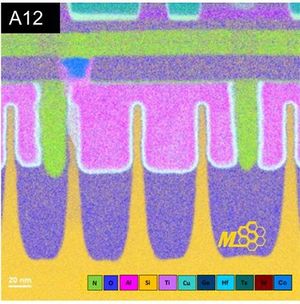
The transistor profile has been enhanced as well. Like Intel's 10 nm process, TSMC introduced cobalt fill at the trench contacts, replacing the tungsten contact. This has the effect of reducing the resistance in that area by 50%. Some of the area scaling and cost benefits were achieved through fin pitch/height scaling. Continuing to scale the fin width gives you a narrower channel while increasing the height to maintain a good effective width is done in order to improve the short channel characteristics and subthreshold slope (i.e., improved Ieff / Ceff) but it also degrades the overall parasitics. Keep in mind that overall, the CV/I device delay is still better because the intrinsic capacitance like the Cgate and Cov still scale with Ieff.
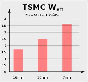
Another way to visualize the effect of the width and height scaling is through the effective width. In the graph shown on the left, we plotted the effective width from TSMC 16 nanometer to the current 7-nanometer node. Compared to N16, N7 has over twice the effective channel width.
Different multi-Vt devices were developed for this process with a Vt range of around 200 mV.
Std Cells[edit]
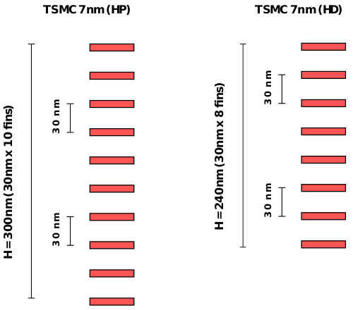
TSMC 7-nanometer (N7 and N7P are the same with this regard) comes in two variations - high density and high performance. Those cells are 240 nm and 300 nm tall respectively. Prior to full production ramp, TSMC originally had a 9T HP variant that relied on a 57-nm CPP. That library was eventually obsoleted in favor of a 64-nm CPP 7.5T library which is now used in mass production by various companies. Note that the 7.5T and 9T are similar in power and performance. Some early designs that started out with a 9T library continued to use it regardless.
| Type | High Density | High Performance | |
|---|---|---|---|
| Name | H240 HD | H300 HP | H360 HP |
| Fin Pitch | 30 nm | ||
| Metal | 40 nm (smallest pitch used with DP) 76 nm (smallest pitch used with SP) | ||
| Gate Pitch | 57 nm | 64 nm | 57 nm |
| Height | 240 nm 8-fin x 30 nm | 300 nm 10-fin x 30 nm | 360 nm 12-fin x 30 nm |
| Tracks | 6 T | 7.5 T | 9 T |
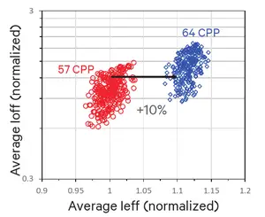
Qualcomm reported that on its own SoC (Snapdragon 855), the high-performance cells deliver around 10-13% higher effective drive current (Ieff), albeit at the cost of being slightly leakier transistors. Based on WikiChip's own analysis, the dense cells come at around 91.2 MTr/mm² while the less dense, high-performance cells, are calculated at around 65 MTr/mm².
N7P[edit]
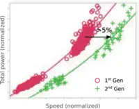
In 2019 TSMC introduced a 2nd-generation N7 process called N7 Performance-enhanced (N7P). N7P is an optimized version of TSMC N7 process. to that end, it remains a DUV-based process, keeping the same design rules and is fully IP-compatible with N7. N7P introduces FEOL and MOL optimizations which are said to translate to either 7% performance improvement at iso-power or up to 10% lower power at iso-speed.
| N7 PPA vs. N7P | ||
|---|---|---|
| Speed @ iso-power | Power @ iso-speed | |
| ~7% | ~10% | |
For their second generation process, TSMC made some additional optimizations, including fin profile optimizations, epi optimizations, MOL resistance optimizations, FEOL capacitance reduction, and metal gate optimizations. Additionally, at the same leakage, at high frequencies, the second-generation 7nm process has improved the Vmin by 50 mV.
N7+[edit]
The N7+ node is TSMC's first process technology to adopt EUV lithography. It is unrelated to both the N7 and N7P processes, and is not IP-compatible with either, requiring re-implementation (new physical layout and validation). N7+ entered mass production in the second quarter of 2019 and uses EUV for four critical layers. Compared to TSMC N7 process, N7+ is said to deliver around 1.2x density improvement. N7+ is also said to deliver 10% higher performance at iso-power or, alternatively, up to 15% lower power at iso-performance. On paper, N7+ appears to be marginally better than N7P, albeit that comes at the cost of re-implementing the design.
| N7 PPA vs. N7+ | ||
|---|---|---|
| Speed @ iso-power | Power @ iso-speed | Density |
| ~10% | ~15% | 1.2x |
Samsung[edit]
Samsung will use EUVL for their 7nm node and thus will be the first to introduce this new technology after more than a decade of development. On May 24 2017, Samsung released a press release of their updated roadmap. Due to delays in the introduction of EUVL, Samsung will introduce a new process called 8nm LPP, to bridge the gap between 10nm and 7nm. The process will be manufactured without the use of EUVL and will feature a slightly relaxed transistor size.
7LPE[edit]
7LPP[edit]
GlobalFoundries[edit]
- Note: As of august 2018 GlobalFoundries has announced they will suspend further development of their 7nm, 5nm and 3nm process.
On May 30 2017, GlobalFoundries Senior Vice President and head of CMOS Business Unit, Gregg Bartlett, announced their updated roadmap. Instead of EUV, the company will use multiple patterning 193i for their 7 nm node. The company is planning on first tape-out in the 2nd half of 2018 with mass production to begin in 2019. Bartlett noted that GF will switch to EUVL when it's ready.
The 7nm process features SAQP for the FEOL, and double patterning for the BEOL. GlobalFoundries claims a 2.8 times density improvement compared to their 14nm process, and a performance improvement of 40% or a 55% reduction in power consumption. Two versions of the process will be developed: a low power version for mobile applications. And a high performance version for desktop and server chips.
7LP[edit]
7HPC[edit]
7 nm Microprocessors[edit]
- PEZY
- MediaTek
- Helio M70
- DImensity 1000
- Dimensity 800U
- Dimensity 1000+
- Dimensity 800
- Apple
- HiSilicon (Huawei)
- Snapdragon (Qualcomm)
- Snapdragon 765G
- 855
- 865
- 870
- Snapdragon 865+
- Exynos (Samsung)
This list is incomplete; you can help by expanding it.
7 nm Microarchitectures[edit]
- AMD
- Ampere
- Esperanto
- Intel
See also[edit]
Bibliography[edit]
- IBM, GlobalFoundries, 2016 IEEE International Interconnect Technology Conference / Advanced Metallization Conference (IITC/AMC).
- Samsung, 2016 IEEE 62nd International Electron Devices Meeting (IEDM).
- TSMC, 2017 IEEE International Solid- State Circuits Conference (ISSCC).
- Qualcomm, TSMC, 2019 Symposia on VLSI Technology and Circuits (VLSI 2019).
 Semiconductor lithography processes technology
