From WikiChip
14 nm lithography process
The 14 nm lithography process is a half-node semiconductor manufacturing process used as a stopgap between the 16 nm and 10 nm processes. As is the case with all recent process nodes, while the term "14 nm" is used by a number of companies, the exact feature sizes various wildly from one manufacturer to another. Commercial integrated circuit manufacturing using 14 nm process began in 2014. This technology is set to be replaced with 10 nm process in 2017.
Contents
Industry
Intel
- 2nd generation finFET transistors
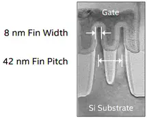
- They are now much more vertical and slimmer, down to 8 nm width.
- TiN pMOS / TiAlN nMOS
- ~22 nm minimum gate length
| Measurement | Scaling from 22 nm | 
| |
| Fin Pitch | 42 nm | 0.70x | |
| Contacted Gate Pitch | 70 nm | 0.78x | |
| Interconnect Pitch (M1P) | 52 nm | 0.65x | |
| SRAM bit cell | 0.0588 µm2 | 0.54x |
Global Foundries / Samsung
- 1st generation finFET transistors
- 2nd generation RMG process
- TiN pMOS WF material / TiAIC nMOS WF material
- Fin height of ~38 nm, width ~8 nm
- ~27 nm minimum gate length
| Measurement | Scaling from 20 nm | Notes | |
| Fin Pitch | 48 nm | ||
| Contacted Gate Pitch | 78 nm | 1.22x | |
| Interconnect Pitch (M1P) | 64 nm | 1.0x | |
| SRAM bit cell | 0.08 µm2 | ?x | High Performance |
| SRAM bit cell | 0.064 µm2 | ?x | High Density |
14 nm Microprocessors
- Intel
This list is incomplete; you can help by expanding it.
14 nm System on Chips
This list is incomplete; you can help by expanding it.
14 nm Microarchitectures
This list is incomplete; you can help by expanding it.
 Semiconductor lithography processes technology