(→5 nm Microprocessors: add Nvidia Grace Hopper CPU) |
|||
| Line 189: | Line 189: | ||
** Dimensity 8100 | ** Dimensity 8100 | ||
** Dimensity 9000 | ** Dimensity 9000 | ||
| + | |||
| + | *Nvidia | ||
| + | ** Grace Hopper | ||
*SAMSUNG | *SAMSUNG | ||
Revision as of 13:29, 26 March 2022
The 5 nanometer (5 nm) lithography process is a technology node semiconductor manufacturing process following the 7 nm process node. Commercial integrated circuit manufacturing using 5 nm process is set to begin sometime around 2020.
The term "5 nm" is simply a commercial name for a generation of a certain size and its technology, and does not represent any geometry of the transistor.
Contents
Overview
First introduced by the major foundries around the 2020 timeframe, the 5-nanometer process technology is characterized by its use of FinFET transistors with fin pitches in the 20s of nanometer and densest metal pitches in the 30s of nanometers. Due to the small feature sizes, these processes make extensive use of EUV for the critical dimensions, along with quad patterning for the fins and double patterning for the rest of the metal stack. Note that Intel 7 nm process is comparable to the foundry 5-nanometer node.
Density
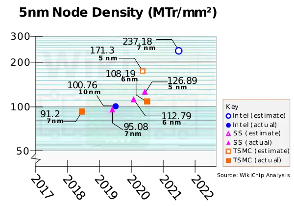
In terms of raw cell-level density, the 5-nanometer node features silicon densities between 130-230 million transistors per square millimeter based on WikiChip's own analysis.
Industry
Only three companies are currently planning or developing a 5-nanometer node: Intel, TSMC, and Samsung.
| Intel | TSMC | Samsung | |||||
|---|---|---|---|---|---|---|---|
| Process | P1278 (CPU), P1279 (SoC) | N5, N5P | 5LPP | ||||
| Production | 2023 | Q1'2020 | 2020 | ||||
| Litho | Lithography | EUV | |||||
| Immersion Exposure | SE (EUV) DP (193i) | SE (EUV) DP (193i) | |||||
| Wafer | Type | Bulk | |||||
| Size | 300 mm | ||||||
| xTor | Type | FinFET | FinFET | ||||
| Voltage | |||||||
| Value | 7 nm Δ | Value | 7 nm Δ | Value | 7 nm Δ | ||
| Fin | Pitch | 27 nm | 1.0x | ||||
| Width | |||||||
| Height | |||||||
| Gate Length (Lg) | 8/10 nm | 1.0x | |||||
| Contacted Gate Pitch (CPP) | 60 nm (HP) 54 nm (HD) | 1.0x 1.0x | |||||
| Minimum Metal Pitch (MMP) | 36 nm | 1.0x | |||||
| SRAM | High-Perf (HP) | 0.032 µm² | 1.0x | ||||
| High-Density (HD) | 0.021 µm² | 0.78x | 0.026 µm² | 1.0x | |||
| Low-Voltage (LV) | |||||||
Intel
P1278
Intel's 5-nanometer (renamed as Intel 20A) process node is expected to ramp around the 2H2024/2025 timeframe.
TSMC
TSMC started mass production of its 5-nanometer N5 node in April 2020. TSMC considers its 5-nanometer node a full node shrink over its 7-nanometer process. In early 2021 TSMC plans on introducing a second version of its N5 process called N5P which provides additional performance enhancements.
N5
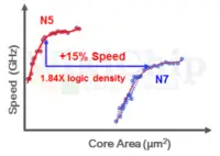
TSMC started its risk production of the 5-nanometer, N5, node in March 2019. The process ramped in April 2020. The N5 process is a full node successor to the company's N7 node, featuring 1.84x improvement in logic density.
The N5 node continues to use bulk silicon FinFET transistors. Leveraging their experience from 7+, 5 nm makes extensive use of EUV for more critical layers in order to reduce the multi-patterning complexity. It is believed that TSMC N5 process uses 11-13 EUV masks in order to replace about 35 immersion layers that would otherwise be required to produce the same pattern without EUV. In other words for TSMC to go from its N7 node to its N5 node would entail going from roughly 87 masks to 115 masks. The introduction of EUV reduced this number back down to around 81 masks.
At a high level, TSMC N5 is a high-density high-performance FinFET process designed for mobile SoCs and HPC applications. Fabrication makes extensive use of EUV at Fab 18, the company’s new 12-inch GigaFab located at the Southern Taiwan Science Park. TSMC says that its 5-nanometer process is 1.84x denser than its 7-nanometer node. TSMC also optimized analog devices where roughly 1.2x scaling has been achieved. TSMC reported the density for a typical mobile SoC which consists of 60% logic, 30% SRAM, and 10% analog/IO, their 5 nm technology scaling was projected to reduce chip size by 35%-40%.
| N5 PPA vs. N7 | ||
|---|---|---|
| Speed @ iso-power | Power @ iso-speed | Max speed improvement @ Vdd (eLVT) |
| ~15% | ~30% | ~25% |
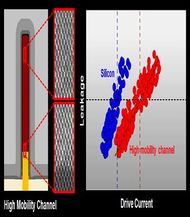
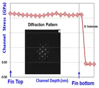
In order to improve the drive current, TSMC introduced a high-mobility channel (HMC) for its 5-nanometer FinFET devices. We believe TSMC is employing a SiGe channel for the pMOS devices. It has been suggested that the channel has 37% Ge composition. TSMC says that the HMC delivers 18% performance gain versus equivalent Si finFETs.
Despite aggressively tighter pitches, TSMC says metal lines RC and via resistance have been kept relatively similar to N7. TSMC says this was achieved by "using EUV patterning, innovative scaled barrier/liner, ESL/ELK dielectrics, and Cu reflow." The improvements meant the interconnect RC did not worsen relative to N7 as N7 did relative to N16.
The 5 nm node is expected to deliver a 15% improvement in performance at constant power or a 20% reduction in power at constant performance. In addition to the ultra-LVT (uLVT) that was offered with N7, there is a new extreme-LVT (eLVT) which can push that 15% up to 25% higher speed at Vdd. Additionally, compared to the standard N5 cells, the HP cell variants can push that performance by another 10% at the cost of density.
The N5 node makes use of a number of density boosters under a marketing term called "smart hyper-scaling features" (similar to Intel). N5 introduces single diffusion breaks in order to reduce cell spacing. Additionally, TSMC added the ability to drop the gate contact over the active region (COAG). Although originally experimented with at the N7 node, via pillars are also used extensively in the N5 node. TSMC makes extensive use of via pillars in N5 due to the three-fold increase of Mx resistance.
SRAM
Two 6T SRAM bitcells were disclosed by TSMC. The high-performance cell is 0.025 µm² while the high-density cell is 0.021 µm². Assuming a ballpark assist circuit overhead of around 30%, the high-density cells yields an estimate of ~32 Mib/mm² of cache. This an increase of 30% from N7 which is around 24.7 Mib/mm². At ISSCC 2020, TSMC presented a test shuttle with 135 Mib of HD SRAM and additional IPs. Their reported density for the HD cells is similar to our estimates.
| N5 Shuttle Test Chip | |
|---|---|
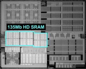
| |
| Technology | 5nm HK-MG FinFET |
| Supply voltage | Core: 0.75V IO: 1.2V |
| Bit cell size | 0.021 μm² |
| SRAM macro configuration | 1024x144 MUX4 256 bits/BL, 288 bits/WL |
| SRAM capacity | 135Mb |
| Test Features | Column Redundancy Programmable E-fuse |
| Die size | 10mm x 7.98mm = 79.8mm2 |
N5P
As with their 7-nanometer process, TSMC will offer an optimized version of their N5 process called N5 Performance-enhanced version (N5P). This process uses the same design rules and is fully IP-compatible with N5. Through FEOL and MOL optimizations, N5P will offer 7% higher performance over N5 at iso-power or 15% lower power at iso-performance. Risk production for N5P is expected to start around the fourth quarter of 2020 with volume production starting sometimes in 2021.
| N5P PPA vs. N5 | ||
|---|---|---|
| Speed @ iso-power | Power @ iso-speed | |
| ~7% | ~15 | |
Samsung
5LPE
Samsung 5-Nanometer Low-Power Early (5LPE) design development completed in early 2019. Unlike TSMC's 5-nanometer node, 5LPE is considered to be only a quarter node successor to the company's 7-nanometer 7LPP process, delivering 1.3x density improvement through a new standard cell library as well as new scaling boosters. Samsung 5LPE process provides different benefits depending on the migration path selected from 7LPP. Moving to a similar 7.5T library will provide 11% performance improvement through various transistor optimizations (Low-k spacer, DC enhancement, etc.). Alternatively, moving to the new 6T library provides around 33% higher density.
| 5LPE PPA vs. 7LPP | ||
|---|---|---|
| Speed @ iso-power | Power @ iso-speed | |
| ~11% | ~20% | |
The area benefits come from a single track reduction in the cell height, contact over the active region edge, and the use of a single diffusion break.
| Samsung 5-nanometer 5LPE Design Rules | ||
|---|---|---|
| Layer | Pitch | Scale Factor |
| Fin | 27 nm | 1.0x |
| Gate Pitch | 54/60 nm | 1.0x |
| Metal 1 | 40 nm | 1.0x |
| Metal 2 | 36 nm | 0.75x |
| Metal 3 | 36 nm | 1.0x |
| Metal 4 | 44 nm | 1.0x |
Samsung 5LPE provides two main libraries - 7.5T library (HD) for performance and a 6T library (UHD) for the area and power optimizations. The 7.5T library utilizes a relaxed 60 nm poly pitch with 10 diffusion lines for a cell height of 270 nanometers. This is identical to the 7LPP library. In the 7LPP process, Samsung also offered a high-density 6.75T cell library with a tighter 54 nm CPP that had 9 diffusion lines. In 5LPP, the new 6T library also utilizes the 54 nm CPP but reduces the diffusion lines to 8 for an even shorter cell height of 216 nm.
| Samsung 5-nanometer 5LPE Standard Libraries | ||
|---|---|---|
| Library | 7.5T HD | 6T UHD |
| Cell Height | 270 nm | 216 nm |
| Config | 3p+3n | 2p+2n |
| Signal Tracks | 6 | 5 |
| CPP | 60 nm | 54 nm |
| M1 | 40 (Bi) | 40 (Uni) |
| M2 | 60 nm | 36 nm |
| DB | MDB | SDB |
| CB | CB on STI | CB on RXN/RXP edge |
With the new 6T library, Samsung is also providing single-fin devices for ultra-low power and always-on circuits.
4LPE
The 4-nanometer Low-Power Early (4LPE) process is a continuation of Samsung's 7LPP and 5LPE, inheriting the transistor and most of the ground rules from 7LPP. This is Samsung's last FinFET-based process. 4LPE features similar pitches to 5LPE but introduces slightly tighter metal pitches.
| Samsung 4-nanometer 4LPE Design Rules | ||
|---|---|---|
| Layer | Pitch | Scale Factor |
| Fin | 27(?) nm | 1.0x(?) |
| Gate Pitch | 54/60 nm | 1.0x |
| Metal 1 | 28 nm | 0.70x |
| Metal 2 | 36 nm | 0.75x |
| Metal 3 | 32 nm | 0.88x |
| Metal 4 | 44 nm | 1.0x |
5 nm Microprocessors
- PEZY
- Apple
- A14 Bionic
- A15 Bionic
- M1
- AMD
- Zen 4
- Navi 3
- MediaTek
- Dimensity 8000
- Dimensity 8100
- Dimensity 9000
- Nvidia
- Grace Hopper
- SAMSUNG
- Exynos 2100
- Exynos 1080
- Exynos W920
- Qualcomm
- Snapdragon 888
- Snapdragon 888+
- Snapdragon 780 5g
- Snapdragon 4000
- Snapdragon 8 Gen 1
- HiSilicon
- Kirin 9000
- Kirin 9000E
This list is incomplete; you can help by expanding it.
5 nm Microarchitectures
This list is incomplete; you can help by expanding it.
Bibliography
- WikiChip Own Research
- TSMC Technology Symposium, 2017
- TSMC Technology Symposium, 2018
- TSMC Technology Symposium, 2019
- Samsung Foundry Forum, 2019
- Samsung, Arm TechCon, 2019
- TSMC, Arm TechCon, 2019
- TSMC, 2019 IEEE 65th International Electron Devices Meeting (IEDM).
 Semiconductor lithography processes technology
