From WikiChip
Difference between revisions of "16 nm lithography process"
(→Industry) |
|||
| Line 31: | Line 31: | ||
| 70 nm || 1.09x | | 70 nm || 1.09x | ||
|- | |- | ||
| − | | 0.07 | + | | 0.07 µm²<ref name="tsmc">Chen, Yen-Huei, et al. "A 16 nm 128 Mb SRAM in High-κ Metal-Gate FinFET Technology With Write-Assist Circuitry for Low-VMIN Applications." IEEE Journal of Solid-State Circuits 50.1 (2015): 170-177.</ref> || 0.55x |
{{scrolling table/end}} | {{scrolling table/end}} | ||
| + | |||
| + | === TSMC === | ||
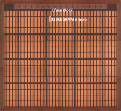
| + | TSMC demonstrated their 256 Mebibit [[SRAM]] wafer from their 7nm HKMG FinFET process. Their chip makes use of 34% of the area of their [[16 nm process]] demo chip counterpart. | ||
| + | {| class="collapsible collapsed wikitable" | ||
| + | |- | ||
| + | ! colspan="2" | TSMC 256Mb SRAM demo wafer<ref name="tsmc" /> | ||
| + | |- | ||
| + | | | ||
| + | <table class="wikitable"> | ||
| + | <tr><th>Technology</th><td>16 nm HK-MG FinFET</td></tr> | ||
| + | <tr><th>Metal scheme</th><td>1P7M</td></tr> | ||
| + | <tr><th>Supply voltage</th><td>0.85 V (core)<br>1.8 V (i/o)</td></tr> | ||
| + | <tr><th>Bit cell size</th><td>0.07 µm²</td></tr> | ||
| + | <tr><th>macro configs</th><td>4096x32 MUX16<br>258 bits/BL<br>272 bits/WL</td></tr> | ||
| + | <tr><th>Capacity</th><td>256 Mib</td></tr> | ||
| + | <tr><th>Test Features</th><td>Row/Column Redundancy<br>Programmable E-fuse</td></tr> | ||
| + | <tr><th>Die Size</th><td>42.6 mm²</td></tr> | ||
| + | </table> | ||
| + | | [[File:tsmc 16nm SRAM block.png|400px]] | ||
| + | |} | ||
== 16 nm Microprocessors== | == 16 nm Microprocessors== | ||
Revision as of 17:08, 10 March 2017
The 16 nanometer (16 nm) lithography process is a full node semiconductor manufacturing process following the 20 nm process stopgap. Commercial integrated circuit manufacturing using 16 nm process began in 2014. The term "16 nm" is simply a commercial name for a generation of a certain size and its technology, as opposed to gate length or half pitch. This technology is set to be replaced with 10 nm process in 2017.
Industry
| Fab |
|---|
| Wafer |
| |
| Fin Pitch |
| Fin Width |
| Fin Height |
| Contacted Gate Pitch |
| Interconnect Pitch (M1P) |
| SRAM bit cell |
TSMC
TSMC demonstrated their 256 Mebibit SRAM wafer from their 7nm HKMG FinFET process. Their chip makes use of 34% of the area of their 16 nm process demo chip counterpart.
| TSMC 256Mb SRAM demo wafer[2] | |||||||||||||||||
|---|---|---|---|---|---|---|---|---|---|---|---|---|---|---|---|---|---|
|

| ||||||||||||||||
16 nm Microprocessors
This list is incomplete; you can help by expanding it.
16 nm Microarchitectures
This list is incomplete; you can help by expanding it.
 Semiconductor lithography processes technology