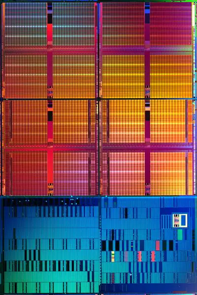
From WikiChip
90 nm lithography process
The 90 nanometer (90 nm) lithography process is a full node semiconductor manufacturing process following the 110 nm process stopgap.
- Commercial integrated circuit manufacturing using 90 nm process began in 2003.
This technology was superseded by the 80 nm (HN) / 65 nm process (FN) in 2006.
Contents
Industry[edit]
Introduced in late 2002, Intel's 90 nm process became the first volume production to introduce strained silicon transistors.
Specifications[edit]
| Fab / Manuf |
|---|
| Process Name |
| 1st Production |
| Type |
| Wafer |
| Metal Layers |
| |
| Contacted Gate Pitch |
| Interconnect Pitch (M1P) |
| SRAM bit cell |
| DRAM bit cell |
| Intel | TSMC | Samsung | Fujitsu | IBM / Toshiba / Sony / AMD |
Motorola | TI | |||||||
|---|---|---|---|---|---|---|---|---|---|---|---|---|---|
| P1262 | CS-100 / CS-101 | HiPerMOS 8 | |||||||||||
| 2002 | 2003 | 2003 | 2004 | 2003 | 2004 | 2005 | |||||||
| Bulk | PDSOI | Bulk | |||||||||||
| 300mm | |||||||||||||
| 7 | 10 | 9 | |||||||||||
| Value | 130 nm Δ | Value | 130 nm Δ | Value | 130 nm Δ | Value | 130 nm Δ | Value | 130 nm Δ | Value | 130 nm Δ | Value | 130 nm Δ |
| 260 nm | 0.82x | 240 nm | 0.77x | 245 nm | 0.70x | ? nm | ?x | ? nm | ?x | ? nm | ?x | ? nm | ?x . |
| 220 nm | 0.63x | 240 nm | 0.71x | 245 nm | 0.70x | ? nm | ?x | ? nm | ?x | ? nm | ?x | ? nm | ?x . |
| 1.0 µm² | 0.50x | 0.999 µm² |
0.47x | 0.999 µm² |
?x | 1.07 µm² | 0.54x | 0.999 µm² |
?x | ? µm² | ?x | ? µm² | ?x |
| 0.275 µm² |
0.19 µm² | ?x | |||||||||||
90 nm Microprocessors[edit]
- AMD
- Cavium
- HAL (Fujitsu)
- IBM
- Loongson
- Qualcomm
- Sun
- Intel
- STMicroelectronics
- STM32 F4
- STM32 F7
- STM32 G0
- STM32 G4
This list is incomplete; you can help by expanding it.
90 nm Microarchitectures[edit]
This list is incomplete; you can help by expanding it.
 Semiconductor lithography processes technology
