From WikiChip
20 nm lithography process
The 20 nanometer (20 nm) lithography process is a half-node semiconductor manufacturing process used as a stopgap between the 22 nm and 16 nm processes. The term "20 nm" is simply a commercial name for a generation of a certain size and its technology, as opposed to gate length or half pitch. Commercial integrated circuit manufacturing using 20 nm process began in 2014. This technology superseded by commercial 16 nm process.
Industry
| Fab |
|---|
| Wafer |
| |
| Contacted Gate Pitch |
| Interconnect Pitch (M1P) |
| SRAM bit cell |
| Samsung | TSMC | ||
|---|---|---|---|
| 300mm | |||
| Value | 28 nm Δ | Value | 28 nm Δ |
| 64 nm | 0.71x | 87 nm | 0.71x |
| 64 nm | 0.67x | 67 nm | 0.70x |
| ? µm² | ?x | 0.081 µm²[1] | 0.64x |
TSMC
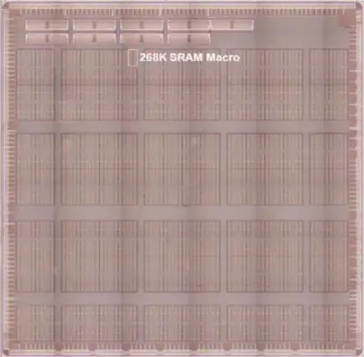
TSMC demonstrated their 112 Mebibit SRAM wafer from their 20 nm HKMG process at the 2013 IEEE ISSCC.
| TSMC 112 Mib SRAM demo 20 nm wafer[1] | |||||||||||||||||
|---|---|---|---|---|---|---|---|---|---|---|---|---|---|---|---|---|---|
|

| ||||||||||||||||
20 nm Microprocessors
- MediaTek
This list is incomplete; you can help by expanding it.
20 nm Microarchitectures
This list is incomplete; you can help by expanding it.
 Semiconductor lithography processes technology