The 7 nanometer (7 nm) lithography process is a full node semiconductor manufacturing process following the 10 nm process node. The term "7 nm" is simply a commercial name for a generation of a certain size and its technology, as opposed to gate length or half pitch. Commercial mass production of integrated circuit using 7 nm process is set to begin sometimes in 2019 or 2020. This technology will be replaced by 5 nm process around 2022.
Industry
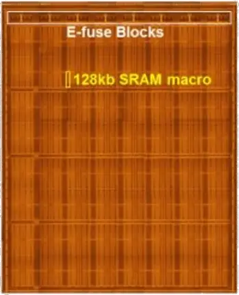
In ISSCC 2017, the memory group at TSMC detailed their test 128 MiB SRAM chip which featured a 42.64 mm² die. The chip is manufactured on TSMC's 7nm HK-MG FinFET process using 4P4E LELELELE patterning technique. The over die is 0.34x smaller than their 16 nm process version. At the same conference, Samsung detailed limited use for EUV in their 7nm node, though not much more is known. On February 8 2017 Intel announced a $7B investment in Arizona's Fab 42 which will eventually produce chips on a 7 nm process.
| Process Name | |
|---|---|
| 1st Production | |
| Lithography | Lithography |
| Immersion | |
| Exposure | |
| Wafer | Type |
| Size | |
| Transistor | Type |
| Voltage | |
| Fin | Pitch |
| Width | |
| Height | |
| Gate Length (Lg) | |
| Contacted Gate Pitch (CPP) | |
| Minimum Metal Pitch (MMP) | |
| SRAM bitcell | High-Perf (HP) |
| High-Density (HD) | |
| Low-Voltage (LV) | |
| DRAM bitcell | eDRAM |
| Intel | TSMC | Common Platform | |||
|---|---|---|---|---|---|
| P1276 (CPU), P1277 (SoC) | |||||
| 193 nm | 193 nm | EUV | |||
| Yes | Yes | ||||
| SAQP | LELELELE | SE | |||
| Bulk | Bulk | Bulk | |||
| 300 nm | 300 nm | 300 nm | |||
| FinFET | FinFET | FinFet | |||
| Value | 10 nm Δ | Value | 10 nm Δ | Value | 10 nm Δ |
| 54 | 0.84x | 48 nm | 0.75x | ||
| 38 | 0.90x | 36 nm | 0.75x | ||
| 0.027 µm² | 0.64x | ||||
TSMC
TSMC demonstrated their 256 Mebibit SRAM wafer from their 7nm HKMG FinFET process. Their chip makes use of 34% of the area of their 16 nm process demo chip counterpart.
7 nm Microprocessors
- MediaTek
This list is incomplete; you can help by expanding it.
7 nm Microarchitectures
This list is incomplete; you can help by expanding it.
References
- Chang, Jonathan, et al. "12.1 A 7nm 256Mb SRAM in high-k metal-gate FinFET technology with write-assist circuitry for low-V MIN applications." Solid-State Circuits Conference (ISSCC), 2017 IEEE International. IEEE, 2017.
- Standaert, T., et al. "BEOL process integration for the 7 nm technology node." Interconnect Technology Conference/Advanced Metallization Conference (IITC/AMC), 2016 IEEE International. IEEE, 2016.
- Samsung/GlobalFoundries, IEEE International Electron Devices Meeting (IEDM) 2016
 Semiconductor lithography processes technology
