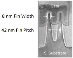
The 14 nanometer (14 nm) lithography process is a semiconductor manufacturing process node serving as shrink from the 22 nm process. The term "14 nm" is simply a commercial name for a generation of a certain size and its technology, as opposed to gate length or half pitch. The 14 nm node was introduced in 2014/2015 and is currently getting replaced by the 10 nm process.
Contents
Industry
| Process Name | |
|---|---|
| 1st Production | |
| Lithography | Lithography |
| Immersion | |
| Exposure | |
| Wafer | Type |
| Size | |
| Transistor | Type |
| Voltage | |
| Fin | Pitch |
| Width | |
| Height | |
| Gate Length (Lg) | |
| Contacted Gate Pitch (CPP) | |
| Minimum Metal Pitch (MMP) | |
| SRAM bitcell | High-Perf (HP) |
| High-Density (HD) | |
| Low-Voltage (LV) | |
| DRAM bitcell | eDRAM |
| Intel | Samsung Alliance Samsung Alliance consists of a process development collaboration between Samsung and GlobalFoundries. GlobalFoundries licenses Samsung's 14nm process at Fab8, New York. |
IBM | UMC | Common Platform Alliance The Common Platform Alliance is a joint collaboration between IBM, STMicroelectronics
| |||||
|---|---|---|---|---|---|---|---|---|---|
| P1272 (CPU) / P1273 (SoC) | 14LPE 1st generation; 14 nm Low Power Early , 14LPP2nd generation; 14 nm Low Power Performance , 14LPC3rd generation; 14 nm Low Power Cost [reduced] , 14LPU4th generation; 14 nm Low Power Ultimate |
14FDSOI | |||||||
| 2014 | 2015 | ||||||||
| 193 nm | 193 nm | 193 nm | 193 nm | 193 nm | |||||
| Yes | Yes | ||||||||
| DP | |||||||||
| Bulk | Bulk | SOI | SOI | ||||||
| 300 mm | 300 mm | 300 mm | 300 mm | 300 mm | |||||
| FinFET | FinFET | FinFET | FinFET | Planar | |||||
| 0.7 V | 0.7 V | 0.8 V | |||||||
| Value | 22 nm Δ | Value | 20 nm Δ | Value | 22 nm Δ | Value | 28 nm Δ | Value | 28 nm Δ |
| 42 nm | 0.70x | 48 nm | N/A | 42 nm | N/A | N/A | |||
| 8 nm | 1.00x | 8 nm | 10 nm | ||||||
| 42 nm | 1.24x | ~38 nm | 25 nm | ||||||
| 20 nm | 0.77x | 30 nm | 20 nm | 0.71x | |||||
| 70 nm | 0.78x | 78 nm | 1.22x | 80 nm | 0.80x | 90 nm | 0.79x | ||
| 52 nm | 0.65x | 64 nm | 1.00x | 64 nm | 0.80x | 64 nm | 0.71x | ||
| 0.0706 µm² | 0.54x | 0.080 µm² | 0.78x | 0.0900 µm² | 0.63x | 0.090 µm² | 0.59x | ||
| 0.0499 µm² | 0.54x | 0.064 µm² | 0.79x | 0.0810 µm² | 0.81x | 0.081 µm² | 0.68x | ||
| 0.0588 µm² | 0.54x | ||||||||
| 0.0174 µm² | 0.67x | ||||||||
Intel
14 nm became Intel's 2nd generation FinFET transistors. Intel uses TiN pMOS / TiAlN nMOS as work function metals. Intel makes use of Self-Aligned Double Patterning (SADP) with 193 nm immersion lithography at critical patterning layers. Compared to all other "14 nm nodes", Intel's process is the densest and considerably so, with >1.5x raw logic density.
Intel improved on their original process with the "14nm+" offering 12% higher drive current. They later improved on that with the "14nm++" process which allows for +23-24% higher drive current for 52% less power. The 14nm++ process also appear to have slightly relaxed the CPP from 70 to 84 nm.
| Intel 14nm Design Rules | ||
|---|---|---|
| Layer | Pitch | Scale Factor |
| Fin | 42 nm | 0.70 |
| Contacted Gate Pitch | 70 nm | 0.78 |
| Metal 0 | 56 | - |
| Metal 1 | 70 | 0.78 |
| Metal 2 | 52 | 0.65 |
Samsung
This process became Samsungs' and GlobalFoundries first generation of FinFET-based transistors. Samsung uses TiN pMOS / TiAIC nMOS as work function metals.
Find models
Click to browse all 14 nm MPU models
14 nm Microprocessors
- Intel
- AMD
- Samsung
This list is incomplete; you can help by expanding it.
14 nm Microarchitectures
This list is incomplete; you can help by expanding it.
Documents
References
- Natarajan, S., et al. "A 14nm logic technology featuring 2 nd-generation FinFET, air-gapped interconnects, self-aligned double patterning and a 0.0588 µm 2 SRAM cell size." Electron Devices Meeting (IEDM), 2014 IEEE International. IEEE, 2014.
- Lin, C. H., et al. "High performance 14nm SOI FinFET CMOS technology with 0.0174 µm 2 embedded DRAM and 15 levels of Cu metallization." Electron Devices Meeting (IEDM), 2014 IEEE International. IEEE, 2014.
- Jan, C-H., et al. "A 14 nm SoC platform technology featuring 2 nd generation Tri-Gate transistors, 70 nm gate pitch, 52 nm metal pitch, and 0.0499 um 2 SRAM cells, optimized for low power, high performance and high density SoC products." VLSI Technology (VLSI Technology), 2015 Symposium on. IEEE, 2015.
- Song, Taejoong, et al. "A 14 nm FinFET 128 Mb SRAM With VMIN Enhancement Techniques for Low-Power Applications." IEEE Journal of Solid-State Circuits 50.1 (2015): 158-169.
- Weber, Olivier, et al. "14nm FDSOI technology for high speed and energy efficient applications." VLSI Technology (VLSI-Technology): Digest of Technical Papers, 2014 Symposium on. IEEE, 2014.
 Semiconductor lithography processes technology
