(→14 nm Microprocessors) |
(→14 nm Microprocessors) |
||
| Line 235: | Line 235: | ||
* {{amd|Ryzen 7}} | * {{amd|Ryzen 7}} | ||
}} | }} | ||
| + | * Samsung | ||
| + | ** {{samsung|Exynos}} | ||
{{expand list}} | {{expand list}} | ||
Revision as of 16:28, 13 May 2017
The 14 nanometer (14 nm) lithography process is a semiconductor manufacturing process node serving as shrink from the 22 nm process. The term "14 nm" is simply a commercial name for a generation of a certain size and its technology, as opposed to gate length or half pitch. The 14 nm node was introduced in 2014/2015 and is currently getting replaced by the 10 nm process.
Contents
Industry
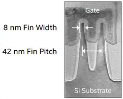
14 nm became Intel's 2nd generation finFET transistors. This process became Samsungs' and GlobalFoundries first generation of finFet-based transistors. Intel uses TiN pMOS / TiAlN nMOS while Samsung uses TiN pMOS / TiAIC nMOS as work function metals. Intel makes use of Self-Aligned Double Patterning (SADP) with 193 nm immersion lithography at critical patterning layers.
| Process Name | |
|---|---|
| 1st Production | |
| Lithography | Lithography |
| Immersion | |
| Exposure | |
| Wafer | Type |
| Size | |
| Transistor | Type |
| Voltage | |
| Fin | Pitch |
| Width | |
| Height | |
| Gate Length (Lg) | |
| Contacted Gate Pitch (CPP) | |
| Minimum Metal Pitch (MMP) | |
| SRAM bitcell | High-Perf (HP) |
| High-Density (HD) | |
| Low-Voltage (LV) | |
| DRAM bitcell | eDRAM |
| Intel | Samsung Alliance Samsung Alliance consists of a process development collaboration between Samsung and GlobalFoundries. GlobalFoundries licenses Samsung's 14nm process at Fab8, New York. |
IBM | UMC | Common Platform Alliance The Common Platform Alliance is a joint collaboration between IBM, STMicroelectronics
| |||||
|---|---|---|---|---|---|---|---|---|---|
| P1272 (CPU) / P1273 (SoC) | 14LPE 1st generation; 14 nm Low Power Early , 14LPP2nd generation; 14 nm Low Power Performance , 14LPC3rd generation; 14 nm Low Power Cost [reduced] , 14LPU4th generation; 14 nm Low Power Ultimate |
14FDSOI | |||||||
| 2014 | 2015 | ||||||||
| 193 nm | 193 nm | 193 nm | 193 nm | 193 nm | |||||
| Yes | Yes | ||||||||
| DP | |||||||||
| Bulk | Bulk | SOI | SOI | ||||||
| 300 mm | 300 mm | 300 mm | 300 mm | 300 mm | |||||
| FinFET | FinFET | FinFET | FinFET | Planar | |||||
| 0.7 V | 0.7 V | 0.8 V | |||||||
| Value | 22 nm Δ | Value | 20 nm Δ | Value | 22 nm Δ | Value | 28 nm Δ | Value | 28 nm Δ |
| 42 nm | 0.70x | 48 nm | N/A | 42 nm | N/A | N/A | |||
| 8 nm | 1.00x | 8 nm | 10 nm | ||||||
| 42 nm | 1.24x | ~38 nm | 25 nm | ||||||
| 20 nm | 0.77x | 30 nm | 20 nm | 0.71x | |||||
| 70 nm | 0.78x | 78 nm | 1.22x | 80 nm | 0.80x | 90 nm | 0.79x | ||
| 52 nm | 0.65x | 64 nm | 1.00x | 64 nm | 0.80x | 64 nm | 0.71x | ||
| 0.0706 µm² | 0.54x | 0.080 µm² | 0.78x | 0.0900 µm² | 0.63x | 0.090 µm² | 0.59x | ||
| 0.0499 µm² | 0.54x | 0.064 µm² | 0.79x | 0.0810 µm² | 0.81x | 0.081 µm² | 0.68x | ||
| 0.0588 µm² | 0.54x | ||||||||
| 0.0174 µm² | 0.67x | ||||||||
Intel
| Intel 14nm Design Rules | ||
|---|---|---|
| Layer | Pitch | Scale Factor |
| Fin | 42 nm | 0.70 |
| Contacted Gate Pitch | 70 nm | 0.78 |
| Metal 0 | 56 | - |
| Metal 1 | 70 | 0.78 |
| Metal 2 | 52 | 0.65 |
Find models
Click to browse all 14 nm MPU models
14 nm Microprocessors
- Intel
- AMD
- Samsung
This list is incomplete; you can help by expanding it.
14 nm Microarchitectures
This list is incomplete; you can help by expanding it.
Documents
References
- Natarajan, S., et al. "A 14nm logic technology featuring 2 nd-generation FinFET, air-gapped interconnects, self-aligned double patterning and a 0.0588 µm 2 SRAM cell size." Electron Devices Meeting (IEDM), 2014 IEEE International. IEEE, 2014.
- Lin, C. H., et al. "High performance 14nm SOI FinFET CMOS technology with 0.0174 µm 2 embedded DRAM and 15 levels of Cu metallization." Electron Devices Meeting (IEDM), 2014 IEEE International. IEEE, 2014.
- Jan, C-H., et al. "A 14 nm SoC platform technology featuring 2 nd generation Tri-Gate transistors, 70 nm gate pitch, 52 nm metal pitch, and 0.0499 um 2 SRAM cells, optimized for low power, high performance and high density SoC products." VLSI Technology (VLSI Technology), 2015 Symposium on. IEEE, 2015.
- Song, Taejoong, et al. "A 14 nm FinFET 128 Mb SRAM With VMIN Enhancement Techniques for Low-Power Applications." IEEE Journal of Solid-State Circuits 50.1 (2015): 158-169.
- Weber, Olivier, et al. "14nm FDSOI technology for high speed and energy efficient applications." VLSI Technology (VLSI-Technology): Digest of Technical Papers, 2014 Symposium on. IEEE, 2014.
 Semiconductor lithography processes technology
