| Line 1: | Line 1: | ||
{{title|Technology Node}}{{lithography processes}} | {{title|Technology Node}}{{lithography processes}} | ||
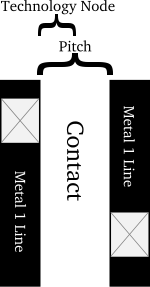
| − | The '''technology node''' (also '''process node''', '''process technology''' or simply '''node''') is traditionally defined as the smallest half-pitch of contacted metal 1 lines allowed in the fabrication process. It is a common metric used to describe and differentiate the technologies used in [[fabricating]] [[integrated circuit]]s. Different nodes often imply different circuit generations and architectures. Generally, the smaller the technology node means the smaller the feature size, producing smaller transistors which are both faster and use less power. Most recently, due to various marketing and discrepancies among foundries, the number itself has lost the exact meaning it once held. | + | The '''technology node''' (also '''process node''', '''process technology''' or simply '''node''') is traditionally defined as the smallest half-pitch of contacted metal 1 lines allowed in the fabrication process. It is a common metric used to describe and differentiate the technologies used in [[fabricating]] [[integrated circuit]]s. Different nodes often imply different circuit generations and architectures. Generally, the smaller the technology node means the smaller the feature size, producing smaller transistors which are both faster and use less power. Most recently, due to various marketing and discrepancies among foundries, the number itself has lost the exact meaning it once held. Recent technology nodes such as [[22 nm]], [[16 nm]], [[14 nm]], and [[10 nm]] refer purely to a specific generation of chips made in a particular technology. It does not correspond to any gate length or half pitch. |
| + | |||
<div style="display:inline-block; float: right;">[[File:tech node.svg|left|150px]]</div> | <div style="display:inline-block; float: right;">[[File:tech node.svg|left|150px]]</div> | ||
The term itself dates back to the 1990s where microprocessors development was driven by higher frequency while [[DRAM]] development was dominated by the evergrowing demand for higher capacities. Since higher capacities were achieved through higher density, it was DRAM that became the driver of [[technology scaling]]. This continued to be the case well into the 2000s. The [[International Technology Roadmap for Semiconductors]] (ITRS) provides the semiconductor industry with guidance and assistance with various technology nodes. By 2006, as microprocessors started dominating the technology scaling, ITRS replaced the term with a number of separate indicators for [[Flash]], [[DRAM]], and [[MPU]]/[[ASCI]]. | The term itself dates back to the 1990s where microprocessors development was driven by higher frequency while [[DRAM]] development was dominated by the evergrowing demand for higher capacities. Since higher capacities were achieved through higher density, it was DRAM that became the driver of [[technology scaling]]. This continued to be the case well into the 2000s. The [[International Technology Roadmap for Semiconductors]] (ITRS) provides the semiconductor industry with guidance and assistance with various technology nodes. By 2006, as microprocessors started dominating the technology scaling, ITRS replaced the term with a number of separate indicators for [[Flash]], [[DRAM]], and [[MPU]]/[[ASCI]]. | ||
Revision as of 19:23, 26 April 2016
The technology node (also process node, process technology or simply node) is traditionally defined as the smallest half-pitch of contacted metal 1 lines allowed in the fabrication process. It is a common metric used to describe and differentiate the technologies used in fabricating integrated circuits. Different nodes often imply different circuit generations and architectures. Generally, the smaller the technology node means the smaller the feature size, producing smaller transistors which are both faster and use less power. Most recently, due to various marketing and discrepancies among foundries, the number itself has lost the exact meaning it once held. Recent technology nodes such as 22 nm, 16 nm, 14 nm, and 10 nm refer purely to a specific generation of chips made in a particular technology. It does not correspond to any gate length or half pitch.
The term itself dates back to the 1990s where microprocessors development was driven by higher frequency while DRAM development was dominated by the evergrowing demand for higher capacities. Since higher capacities were achieved through higher density, it was DRAM that became the driver of technology scaling. This continued to be the case well into the 2000s. The International Technology Roadmap for Semiconductors (ITRS) provides the semiconductor industry with guidance and assistance with various technology nodes. By 2006, as microprocessors started dominating the technology scaling, ITRS replaced the term with a number of separate indicators for Flash, DRAM, and MPU/ASCI.
Half node
Half node, much like the process term also dates to the 1990s when incremental shrinkage was readily achievable. A full technology node was expected to have a linear scaling shrink of 0.7x (e.g. 130 nm after a full shrink yields 90 nm). Similarly, the associated half node was then expected to have a 0.9x linear shrink. The premise of this idea is that when a new technology node was being considered for a new full node, foundries design rules (e.g. standard cells) were carefully designed with the expectation that a half node shrink was to follow after 18 months. When a half shrink finally took place, it was a just matter of various readjustments. Proper planning and proactive considerations during circuit design stages could allow seamless transition to the new process without encountering design rule violations, timing, or otherwise any reliability issues. Note that some steps such as packaging do need to be redesigned.
| This article is still a stub and needs your attention. You can help improve this article by editing this page and adding the missing information. |
 Semiconductor lithography processes technology
