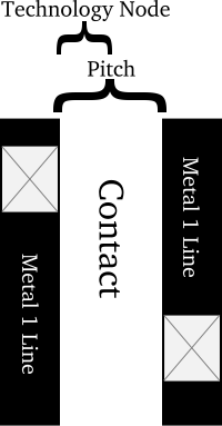
The technology node (also process node, process technology or simply node) is traditionally defined as the smallest half-pitch of contacted metal 1 lines allowed in the fabrication process. It is a common metric used to describe and differentiate the technologies used in fabricating integrated circuits. Different nodes often imply different circuit generations and architectures. Generally, the smaller the technology node means the smaller the feature size, producing smaller transistors which are both faster and use less power. Most recently, due to various marketing and discrepancies among foundries, the number itself has lost the exact meaning it once held.
The term itself dates back to the 1990s where microprocessors development was driven by higher frequency while DRAM development was dominated by the evergrowing demand for higher capacities. Since higher capacities were achieved through higher density, it was DRAM that became the driver of technology scaling. This continued to be the case well into the 2000s.
The International Technology Roadmap for Semiconductors (ITRS) provides the semiconductor industry with guidance and assistance with various technology nodes. By 2006, as microprocessors started dominating the technology scaling, ITRS replaced the term with a number of separate indicators for Flash, DRAM, and MPU/ASCI.
| This article is still a stub and needs your attention. You can help improve this article by editing this page and adding the missing information. |
 Semiconductor lithography processes technology
