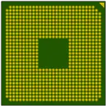
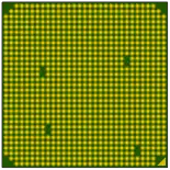
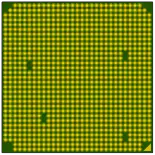
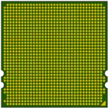
From WikiChip
List of AMD CPU sockets
Contents
Overview
| Year | Desktop | Desktop APU | Server | Mobile | Tablet | Embedded |
|---|---|---|---|---|---|---|
| 1998 | Super 7 | Super 7 | ||||
| 1999 | Slot A | |||||
| 2000 | Socket A | Socket A | ||||
| 2003 | 754, 940 | 940 | 563, 754 | |||
| 2004 | 939 | |||||
| 2006 | AM2, Fr3 | F | S1g1 | |||
| 2007 | AM2+ | Fr2 | ||||
| 2008 | Fr5 | S1g2 | ||||
| 2009 | AM3 | Fr6 | S1g3 | ASB1 | ||
| 2010 | C32, G34 | S1g4 | ASB2 | |||
| 2011 | FM1 | FS1 | FT1 | FT1 | ||
| 2012 | AM3+ | FM2 | FS1r2, FP2 | FP2 | ||
| 2013 | FT3 | FT3 | ||||
| 2014 | FM2+, AM1 | FP3 | FT3b | FP3, FT3b, SP1 | ||
| 2015 | FP4 | FP4 | ||||
| 2016 | AM4 | AM4 | FT4 | |||
| 2017 | TR4 | SP3 | ||||
| 2018 | FP5 | FP5, SP4, SP4r2 | ||||
| 2019 | sTRX4 | |||||
| 2020 | sWRX8 | FP6 | FT5 | FP6 | ||
| 2022 | AM5 | AM5 | SP5 |
Desktop/HEDT/Workstation Sockets
| Name (a.k.a.) | Year | Type[1] | Contacts | x86 CPU Family | MC[2] | I/O lanes[3] | APU[4] | FCH[5] | Notes | Package[6] |
|---|---|---|---|---|---|---|---|---|---|---|
| Super Socket 7 | 1998 | PGA | 321 | 5 | - | FSB | ✘ | - | 
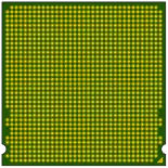
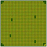
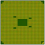
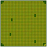
| |
| Slot A | 1999 | SEC | 242 | 6 | - | FSB | ✘ | - | ||
| Socket A | 2000 | PGA | 462 | 6 | - | FSB | ✘ | - | 
| |
| Socket 563 | 2003 | PGA | 563 | 6 | - | FSB | ✘ | - | 
| |
| Socket 754 | 2003 | PGA | 754 | 0Fh | 72 bit DDR | 16 HT1 | ✘ | - | 
| |
| Socket 940 | 2003 | PGA | 940 | 0Fh | 144 bit DDR | 3 × 16 HT1 | ✘ | - |  
| |
| Socket 939 | 2004 | PGA | 939 | 0Fh | 144 bit DDR | 16 HT1 | ✘ | - | 
| |
| Socket AM2 | 2006 | PGA | 940 | NPT 0Fh | 144 bit DDR2 | 16 HT1 | ✘ | - | 
| |
| Socket Fr3 | 2006 | LGA | 1207 | NPT 0Fh | 2 × 72 bit DDR2 | 3 × 16 HT1 | ✘ | - | 
| |
| Socket AM2+ (AM2r2) | 2007 | PGA | 940 | 10h | 2 × 72 bit DDR2 | 16 HT3 | ✘ | - | 
| |
| Socket AM3 | 2009 | PGA | 938 | 10h | 2 × 72 bit DDR2/3 | 16 HT3 | ✘ | - |  
| |
| Socket FM1 | 2011 | PGA | 905 | 12h | 2 × 72 bit DDR3 | 16 + 4 PCIe2 | ✔ | 4 PCIe2 | 
| |
| Socket AM3+ (AM3b) | 2012 | PGA | 941 | 15h | 2 × 72 bit DDR3 | 16 HT3 | ✘ | - | 
| |
| Socket FM2 | 2012 | PGA | 904 | 15h | 2 × 64 bit DDR3 | 16 + 4 PCIe2 | ✔ | 4 PCIe2 | 
| |
| Socket AM1 (FS1b) | 2014 | PGA | 721 | 16h | 72 bit DDR3 | 4 + 4 PCIe2 | ✔ | integrated | 
| |
| Socket FM2+ (FM2b, FM2r2) | 2014 | PGA | 906 | 15h | 2 × 64 bit DDR3 | 16 + 4 PCIe2/3 | ✔ | 4 PCIe2 | 
| |
| Socket AM4 | 2016 | PGA | 1331 | 15h, 17h, 19h | 2 × 72 bit DDR3/4 | 16 + 4 PCIe3/4 | ✔ | 4 PCIe3/4 | 
| |
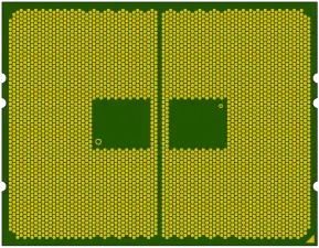
| Socket TR4 (SP3r2) | 2017 | LGA | 4094 | 17h | 4 × 72 bit DDR4 | 4 × 16 PCIe3 | ✘ | 
| ||
| Socket sTRX4 | 2019 | LGA | 4094 | 17h | 4 × 72 bit DDR4 | 4 × 16 PCIe4 | ✘ | 
| ||
| Socket sWRX8 | 2020 | LGA | 4094 | 17h, 19h | 8 × 72 bit DDR4 | 8 × 16 PCIe4 | ✘ | 
| ||
| Socket AM5 | 2022 | LGA | 1718 | 19h | 2 × 72 bit DDR5 | 16 + 4 + 4 PCIe4/5 | ✔ | 4 PCIe4/5 | 
|
- ↑ PGA = Pin Grid Array, BGA = Ball Grid Array (CPU package soldered directly to the motherboard), LGA = Land Grid Array, SEC = Single Edge Cartridge (printed circuit board with an edge connector similar to graphics cards).
- ↑ If processors for this socket integrate a Memory Controller, the number of independent channels times the maximum channel width in bits, including ECC lanes. Not all processors for this socket may support ECC.
- ↑ FSB = Front Side Bus (memory and I/O interfaces provided by the chipset), HTx = HyperTransport generation x link (I/O interfaces provided by the chipset), PCIex = Peripheral Component Interconnect Express generation x link. Note HT and PCIe links support bifurcation, e.g. 1x16 into 2x8 links. The table lists the maximum number of lanes and interfaces. Some processors may support fewer, and some motherboards may use alternative functions of these pins.
- ↑ This socket has graphics interfaces (DisplayPort, HDMI, VGA, etc.) to accommodate Accelerated Processing Units i.e. processors with integrated graphics. Not all processors for this socket may integrate a graphics processor.
- ↑ The number of dedicated I/O lanes to the Fusion Controller Hub a.k.a. chipset, equivalent to Intel's Platform Controller Hub. The FCH mainly serves as an I/O expander. A controller hub may be integrated on the processor, in this case the CPU package and socket has suitable I/O interfaces (USB, SATA, LPC, SMBus, etc.), sometimes in addition to the FCH interface.
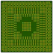
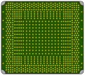
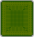
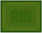
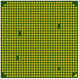
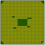
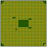
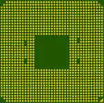
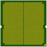
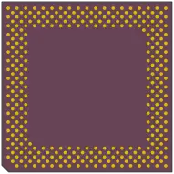
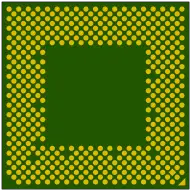
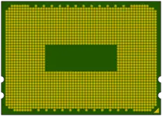
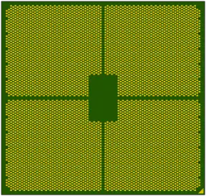
- ↑ CPU package bottom view, not to scale.
Server Sockets
| Name | Year | Type | Contacts | Fam. | MC | I/O lanes | APU | SCH | Notes | Package |
|---|---|---|---|---|---|---|---|---|---|---|
| Socket 940 | 2003 | PGA | 940 | 0Fh | 144 bit DDR | 3 × 16 HT1 | ✘ | - |  
| |
| Socket F | 2006 | LGA | 1207 | NPT 0Fh | 2 × 72 bit DDR2 | 3 × 16 HT1 | ✘ | - | 
| |
| Socket Fr2 | 2007 | LGA | 1207 | NPT 0Fh, 10h | 2 × 72 bit DDR2 | 3 × 16 HT1 | ✘ | - | 
| |
| Socket Fr5 | 2008 | LGA | 1207 | NPT 0Fh, 10h | 2 × 72 bit DDR2 | 3 × 16 HT1/3 | ✘ | - | 
| |
| Socket Fr6 | 2009 | LGA | 1207 | 10h | 2 × 72 bit DDR2 | 3 × 16 HT3 | ✘ | - | 
| |
| Socket C32 | 2010 | LGA | 1207 | 10h, 15h | 2 × 72 bit DDR3 | 3 × 16 HT3 | ✘ | - | 
| |
| Socket G34 | 2010 | LGA | 1944 | 10h, 15h | 4 × 72 bit DDR3 | 3 × 16 + 2 × 8 HT3 | ✘ | - | 
| |
| Socket SP3 | 2017 | LGA | 4094 | 17h, 19h | 8 × 72 bit DDR4 | 8 × 16 PCIe3/4 | ✘ | integrated | 
| |
| Socket SP5 | 2022 | LGA | 6096 | 19h | 12 × 80 bit DDR5 | 8 × 16 PCIe5 | ✘ | integrated | 
|
Mobile Sockets (mainstream)
| Name | Year | Type | Pins | Fam. | MC | I/O lanes | APU | FCH | Notes | Package |
|---|---|---|---|---|---|---|---|---|---|---|
| Super Socket 7 | 1998 | PGA | 321 | 5 | - | FSB | ✘ | - | 
| |
| Socket A | 2000 | PGA | 462 | 6 | - | FSB | ✘ | - | 
| |
| Socket 563 | 2003 | PGA | 563 | 6 | - | FSB | ✘ | - | 
| |
| Socket 754 | 2003 | PGA | 754 | 0Fh | 72 bit DDR | 16 HT1 | ✘ | - | 
| |
| Socket S1g1 | 2006 | PGA | 638 | NPT 0Fh | 144 bit DDR2 | 16 HT1 | ✘ | - | 
| |
| Socket S1g2 | 2008 | PGA | 638 | 11h | 2 × 64 bit DDR2 | 16 HT3 | ✘ | - | 
| |
| Socket S1g3 | 2009 | PGA | 638 | 10h | 2 × 64 bit DDR2 | 16 HT3 | ✘ | - | 
| |
| Package ASB1 | 2009 | BGA | 812 | NPT 0Fh | 144 bit DDR2 | 16 HT1 | ✘ | - | 
| |
| Socket S1g4 | 2010 | PGA | 638 | 10h | 2 × 64 bit DDR3 | 16 HT3 | ✘ | - | 
| |
| Package ASB2 | 2010 | BGA | 812 | 10h | 2 × 72 bit DDR3 | 16 HT3 | ✘ | - | 
| |
| Socket FS1 | 2011 | PGA | 722 | 12h | 2 × 64 bit DDR3 | 16 + 4 PCIe2 | ✔ | 4 PCIe2 | 
| |
| Socket FS1r2 | 2012 | PGA | 722 | 15h | 2 × 64 bit DDR3 | 16 + 4 PCIe2 | ✔ | 4 PCIe2 | 
| |
| Package FP2 | 2012 | BGA | 827 | 15h | 2 × 64 bit DDR3 | 16 + 4 PCIe2 | ✔ | 4 PCIe2 | 
| |
| Package FP3 | 2014 | BGA | 854 | 15h | 2 × 72 bit DDR3 | 16 + 8 PCIe2/3 | ✔ | 4 PCIe2 | ||
| Package FP4 | 2015 | BGA | 968 | 15h, 16h | 2 × 72 bit DDR3/4 | 8 + 4 PCIe3 | ✔ | integrated | 
| |
| Package FP5 | 2018 | BGA | 1140 | 17h | 2 × 72 bit DDR4 | 8 + 8 PCIe3 | ✔ | integrated | 
| |
| Package FP6 | 2020 | BGA | 1140 | 17h | 2 × 72 bit DDR4 4 × 32 bit LPDDR4x |
8 + 12 PCIe3 | ✔ | integrated | 
|
Mobile Sockets (ultrathin, tablet)
| Name | Year | Type | Pins | Fam. | MC | I/O lanes | APU | FCH | Notes | Package |
|---|---|---|---|---|---|---|---|---|---|---|
| Package FT1 | 2011 | BGA | 413 | 14h | 64 bit DDR3 | 4 PCIe2 | ✔ | 4 PCIe2 | 
| |
| Package FT3 | 2013 | BGA | 769 | 16h | 72 bit DDR3 | 4 PCIe2 | ✔ | 4 PCIe2 | 
| |
| Package FT3b | 2014 | BGA | 769 | 16h | 72 bit DDR3 | 4 PCIe2 | ✔ | 4 PCIe2 | 
| |
| Package FT4 | 2016 | BGA | 769 | 15h | 64 bit DDR3/4 | 8 PCIe3 | ✔ | integrated | 
| |
| Package FT5 | 2020 | BGA | 17h | 2 × ?? bit DDR4 | 8 PCIe3 | ✔ | integrated |
Embedded Sockets
| Name | Year | Type | Pins | Fam. | MC | I/O lanes | APU | FCH | Notes | Package |
|---|---|---|---|---|---|---|---|---|---|---|
| Package ASB1 | 2009 | BGA | 812 | NPT 0Fh | 144 bit DDR2 | 16 HT1 | ✘ | - | 
| |
| Package ASB2 | 2010 | BGA | 812 | 10h | 2 × 72 bit DDR3 | 16 HT3 | ✘ | - | 
| |
| Package FT1 | 2011 | BGA | 413 | 14h | 64 bit DDR3 | 4 PCIe2 | ✔ | 4 PCIe2 | 
| |
| Package FP2 | 2012 | BGA | 827 | 15h | 2 × 64 bit DDR3 | 16 + 4 PCIe2 | ✔ | 4 PCIe2 | 
| |
| Package FT3 | 2013 | BGA | 769 | 16h | 72 bit DDR3 | 4 PCIe2 | ✔ | 4 PCIe2 | 
| |
| Package FP3 | 2014 | BGA | 854 | 15h | 2 × 72 bit DDR3 | 16 + 8 PCIe2/3 | ✔ | 4 PCIe2 | ||
| Package SP1 | 2014 | BGA | 1021 | 2 × 72 bit DDR3/4 | 8 PCIe3 | ✘ | integrated | |||
| Package FT3b | 2014 | BGA | 769 | 16h | 72 bit DDR3 | 4 PCIe2 | ✔ | 4 PCIe2 | 
| |
| Package FP4 | 2015 | BGA | 968 | 15h, 16h | 2 × 72 bit DDR3/4 | 8 + 4 PCIe3 | ✔ | integrated | 
| |
| Package FP5 | 2018 | BGA | 1140 | 17h | 2 × 72 bit DDR4 | 8 + 8 PCIe3 | ✔ | integrated | 
| |
| Socket SP3 | 2017 | LGA | 4094 | 17h | 8 × 72 bit DDR4 | 8 × 16 PCIe3 | ✘ | integrated | [1] | 
|
| Package SP4 | 2018 | BGA | 17h | 4 × 72 bit DDR4 | 4 × 16 PCIe3 | ✘ | integrated | |||
| Package SP4r2 | 2018 | BGA | 17h | 2 × 72 bit DDR4 | 2 × 16 PCIe3 | ✘ | integrated | |||
| Package FP6 | 2020 | BGA | 1140 | 17h | 2 × 72 bit DDR4 4 × 32 bit LPDDR4x |
8 + 12 PCIe3 | ✔ | integrated | 
|
- ↑ Embedded versions of EPYC 7001 & 7002 processors, hence Family 17h only.
Game Consoles
| Name | Year | Type | Pins | Fam. | MC | I/O | APU | FCH | Notes |
|---|---|---|---|---|---|---|---|---|---|
| Xbox One X | 2017 | BGA | 2409 | 16h | 12 × 32 bit GDDR5 | 8 PCIe3 | ✔ | integrated | Lidless package with stiffener frame, 50 mm × 50 mm, 0.8+ mm multi-pitch[1] |
| Xbox Series X/S | 2020 | BGA | 2963 | 17h | 20 × 16 bit GDDR6 | 8 PCIe4 | ✔ | integrated | Lidless package with stiffener frame, 52.5 mm × 52.5 mm, 0.8+ mm multi-pitch[1] |
- ↑ 1.0 1.1 Paternoster, Paul et al. (2021). XBOX Series X: A Next-Generation Gaming Console SoC. Proceedings of IEEE ISSCC 2021. pp. 46-48. doi:10.1109/ISSCC42613.2021.9366057


