| Edit Values | |
| Socket AM2 | |
| General Info | |
| Designer | AMD |
| Introduction | May 23, 2006 (launched) |
| Market | Desktop |
| Microarchitecture | K8 |
| TDP | 125 W 125,000 mW 0.168 hp 0.125 kW |
| Package | |
| Name | OPGA-940 AM2 |
| Type | Organic Micro Pin Grid Array |
| Contacts | 940 |
| Dimension | 40.0 mm 4 cm × 40.0 mm1.575 in 4 cm 1.575 in |
| Pitch | 1.27 mm 0.05 in |
| Socket | |
| Name | Socket AM2 |
| Type | PGA |
Socket AM2 was the socket for OPGA-940 and OPGA-938-packaged AMD microprocessors with an integrated DDR2 memory controller and the successor to Socket 939. Socket AM2 targets the performance, mainstream, and value desktop segment. Its contemporaries are Socket S1 for mobile processors and Socket F for the server and workstation market. For the small form factor desktop, mobile and embedded market AMD developed package ASB1. Socket AM2 was superseded by Socket AM2+.
The OPGA-940 package for Socket AM2 is compatible with Socket AM2+. The package has the same dimensions but is mechanically, due to keying, and electrically incompatible with Socket 939 for processors with a DDR memory controller, Socket 940 for first generation Opteron processors, and Socket AM3 and AM3+ for processors with a DDR3 memory controller.
Socket AM2+ processors in the OPGA-940 package and Socket AM3 processors in the OPGA-938 package are compatible with Socket AM2, subject to the motherboard recognizing the CPU and the limitations of Socket AM2.
All processors for Socket AM2 belong to AMD's NPT Family 0Fh and use the K8 microarchitecture.
Contents
Features[edit]
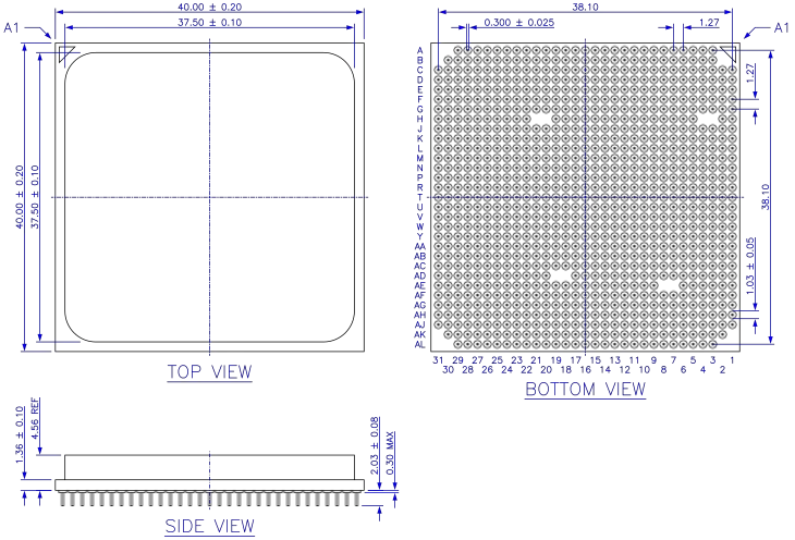
- 940-pin lidded micro pin grid array package, 1.27 mm pitch, 31 × 31 pins, 40 × 40 mm, organic substrate
- 16 bit HyperTransport 1.0 interface up to 1 GHz, 2000 MT/s, 4 Gbyte/s in each direction
- 128/144 bit DDR2 SDRAM interface up to 400 MHz, PC-6400 (DDR2-800), 12.8 Gbyte/s
- Up to 4 UDIMMs (2 per channel), up to 4 Gbyte per UDIMM, SEC-DED ECC
- JEDEC SSTL_1.8
- P-States, ACPI C1, C1E (NPT Family 0Fh Rev. G and later processors), C2, S3, S5
- Thermal diode, overtemperature protection
Chipsets[edit]
- AMD 580, 690, 700 series
- Nvidia nForce3, nForce4, nForce 400 series, nForce 500 series, nForce 630a, GeForce 8000 series
- SiS 761GX, 771
- VIA K8T890, K8M890, K8T900
Processors using Socket AM2[edit]
- AMD Opteron codename "Santa Ana", "Budapest"
- AMD Athlon 64 FX "Windsor"
- AMD Athlon 64 X2 "Windsor", "Brisbane"
- AMD Athlon "Orleans", "Lima"
- AMD Sempron X2 "Brisbane"
- AMD Sempron "Manila", "Sparta"
- AMD Athlon Neo X2
| List of all Socket AM2-based Processors | |||||||||||||||||||
|---|---|---|---|---|---|---|---|---|---|---|---|---|---|---|---|---|---|---|---|
| Model | Price | Process | Launched | µarch | Family | Core | C | T | Freq | Turbo | TDP | ||||||||
| Count: 0 | |||||||||||||||||||
Package Diagram[edit]
OPGA-940 package for Socket AM2/AM2+. All dimensions in millimeters.
Socket Outline[edit]
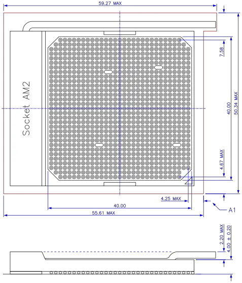
All dimensions in millimeters.
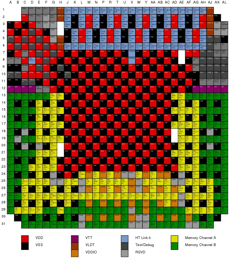
Pin Map[edit]
Pin Description[edit]
| Signal | Description |
|---|---|
| CLKIN_H/L | 200 MHz Differential PLL Reference Clock |
| CPU_PRESENT_L | Processor is present |
| DBREQ_L, DBRDY | Debug Request/Ready |
| HTREF0, HTREF1 | HyperTransport Compensation Resistor to VSS, VLDT |
| L0_CADIN/OUT_H/L[15:0] | HT Link 0 Differential Command/Address/Data Input/Output |
| L0_CLKIN/OUT_H/L[1:0] | HT Link 0 Differential Clock Input/Output |
| L0_CTLIN_H/L[1:0] | HT Link 0 Differential Control Input/Output |
| LDTSTOP_L | HT Stop Control Input for power management and link width and frequency change |
| MA0/MA1/MB0/MB1_CLK_H/L[2:0] | DRAM Differential Clock |
| MA0/MA1/MB0/MB1_CS_L[1:0] | DRAM Chip Select |
| MA0/MA1/MB0/MB1_ODT[0] | DRAM Enable Pin for On Die Termination |
| MA/MB_ADD[15:0] | DRAM Column/Row Address |
| MA/MB_BANK[2:0] | DRAM Bank Address |
| MA/MB_CAS_L | DRAM Column Address Strobe |
| MA/MB_CHECK[7:0] | DRAM ECC Bits |
| MA/MB_CKE[1:0] | DRAM Clock Enable |
| MA/MB_DATA[63:0] | DRAM Data Bus |
| MA/MB_DM[8:0] | DRAM Data Mask |
| MA/MB_DQS_H/L[8:0] | DRAM Differential Data Strobe |
| MA/MB_RAS_L | DRAM Row Address Strobe |
| MA/MB_WE_L | DRAM Write Enable |
| M_VREF | DRAM Interface Voltage Reference |
| M_ZP, M_ZN | Compensation Resistor to VSS, VDDIO |
| PROCHOT_L | Processor in HTC-active state input/output |
| PSI_L | Power Status Indicator (low power state) for VDD regulator |
| PWROK | Voltages and CLKIN have reached specified operation |
| RESET_L | Processor Reset |
| RSVD | Reserved |
| SIC, SID | Sideband (APML/SBI/SMBus) Temperature Sensor Interface Clock, Data |
| TCK, TDI, TDO, TMS, TRST_L | JTAG interface |
| TEST* | Test signal |
| THERMDA, THERMDC | Thermal Diode Anode, Cathode |
| THERMTRIP_L | Thermal Sensor Trip output |
| VDD | Core power supply |
| VDD_FB_H/L | Differential feedback to VDD regulator |
| VDDA | Filtered PLL supply voltage |
| VDDIO | DRAM I/O ring power supply |
| VDDIO_FB_H/L | Differential feedback to VDDIO regulator |
| VID[5:0] | Voltage ID for VDD regulator |
| VLDT_A/B | HyperTransport I/O ring power supply |
| VSS | Ground |
| VTT | DRAM Termination voltage |
| VTT_SENSE | VTT monitor pin |
References[edit]
- "Socket AM2 Design Specification", AMD Publ. #31875, Rev. 3.00, May 2008
- "BIOS and Kernel Developer’s Guide for AMD NPT Family 0Fh Processors", AMD Publ. #32559, Rev. 3.16, November 2009
- "AMD Opteron™ Processor Product Data Sheet", AMD Publ. #23932, Rev. 3.23, March 2007
- "AMD Athlon™ 64 Processor Product Data Sheet", AMD Publ. #24659, Rev. 3.18, September 2006
- "AMD Athlon™ 64 FX Product Data Sheet", AMD Publ. #30431, Rev. 3.16, September 2006
- "AMD Sempron™ Processor Product Data Sheet", AMD Publ. #31805, Rev. 3.05, September 2006
- "AMD Athlon™ 64 X2 Dual-Core Processor Product Data Sheet", AMD Publ. #33425, Rev. 3.10, January 2007
- "Revision Guide for AMD NPT Family 0Fh Processors", AMD Publ. #33610, Rev. 3.48, December 2011
See also[edit]
| designer | AMD + |
| first launched | May 23, 2006 + |
| instance of | package + |
| market segment | Desktop + |
| microarchitecture | K8 + |
| name | Socket AM2 + |
| package | OPGA-940 AM2 + |
| package contacts | 940 + |
| package length | 40 mm (4 cm, 1.575 in) + |
| package pitch | 1.27 mm (0.05 in) + |
| package type | Organic Micro Pin Grid Array + |
| package width | 40 mm (4 cm, 1.575 in) + |
| socket | Socket AM2 + |
| tdp | 125 W (125,000 mW, 0.168 hp, 0.125 kW) + |


