| Edit Values | |
| Socket SP5 | |
| General Info | |
| Designer | AMD |
| Introduction | November 10, 2022 (launched) |
| Market | Server |
| Microarchitecture | Zen 4 |
| TDP | 400 W 400,000 mW 0.536 hp 0.4 kW |
| Package | |
| Name | SP5, FCLGA-6096 |
| Type | FC-OLGA |
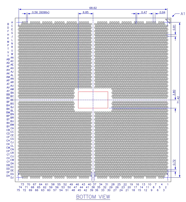
| Contacts | 6096 |
| Dimension | 75.4 mm 7.54 cm × 72 mm2.969 in 7.2 cm 2.835 in |
| Pitch | 0.81 mm 0.0319 in × 0.94 mm0.037 in |
| Socket | |
| Name | Socket SP5 |
| Type | SM-LGA |
| Succession | |
Socket SP5 is a microprocessor socket designed by AMD for the fourth generation of their EPYC family of high performance server processors, succeeding Socket SP3. Its counterpart for desktop processors is Socket AM5.
Contents
Overview[edit]
Socket SP5 is a zero insertion force, heatsink actuated, surface-mount LGA (land grid array) socket for use with a 6096-contact, 0.94 mm × 0.81 mm interstitial pitch, organic land grid array CPU package.
It supports 12 channels of DDR5 memory with two 40-bit subchannels (32 bit data + 8 bit ECC) and up to 2 DIMMs per channel, eight 16-lane PCIe Gen 5 I/O links, three or four of which are repurposed as inter-socket links on dual socket systems, two 4-lane PCIe Gen 3 links, four USB 3.1 Gen 1 ports, and up to 32 SATA Gen 3 ports.
This compares to eight 72-bit DDR4 channels and eight 16-lane PCIe Gen 3/4 links on its predecessor Socket SP3. :(SP4 and SP4r2 are BGA (ball grid array) packages of EPYC 3000 embedded processors.)
The following AMD processor families use Socket SP5:
| CPU Family | Microarch. | Process | Products | |
|---|---|---|---|---|
| Type 0 | Family 19h Models 10h–1Fh | Zen 4 | 5 nm | EPYC 9004 "Genoa" (Model 11h) |
The codename of AMD's SP5 reference platform (CRB) is "Titanite".
Package Description[edit]
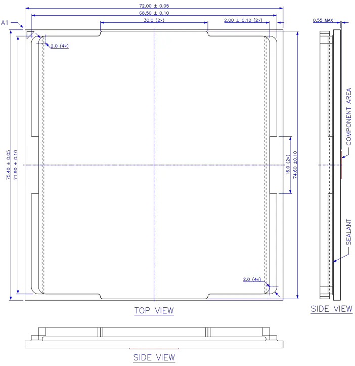
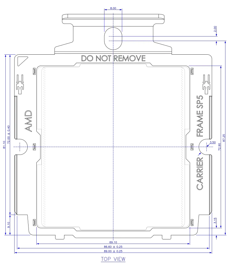
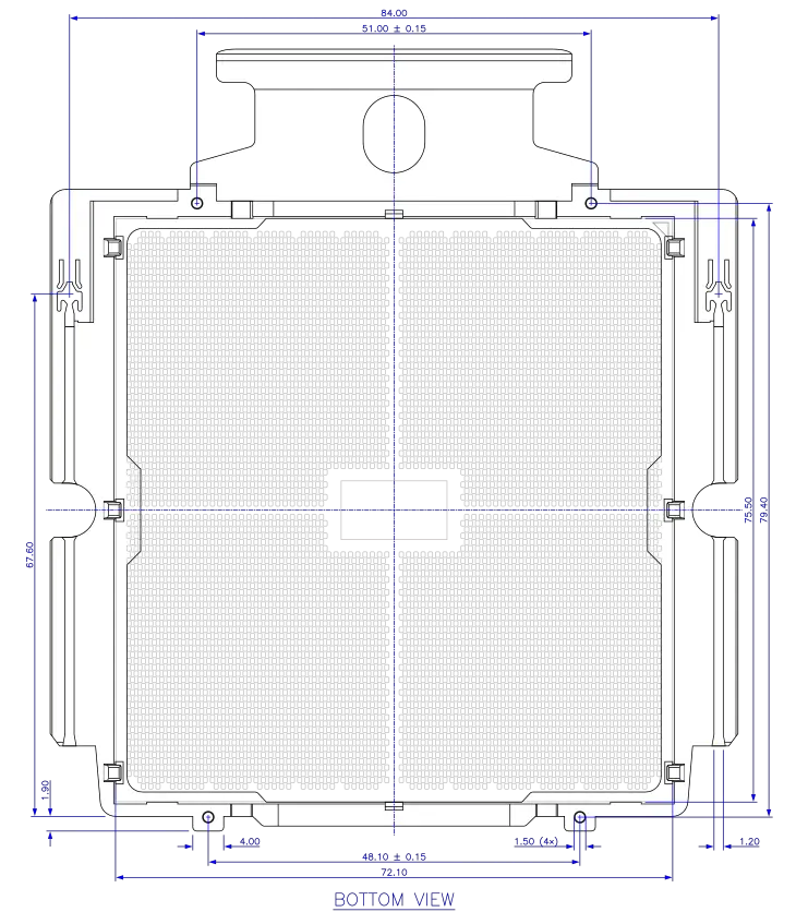
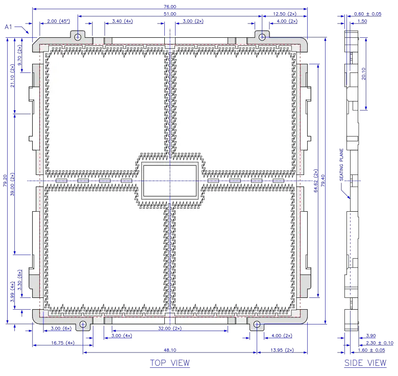
The SP5 CPU package is lidded, has a 72 mm × 75.4 mm organic substrate with flip chip die attachment, 6096 land pads with gold over nickel plating, and leaves AMD's OSAT partner in a shipping tray with a carrier frame pre-installed. The carrier frame is a part of the package loading mechanism and remains on the package in the socket.
The package has the same length (75.4 mm) as the Socket SP3 package but no keying notches and a redesigned lid bridging the chiplets and decoupling capacitors on the package top with flanges on only two sides, providing more space for these components. Additional components are placed on the package bottom side. While the package has no apparent anti-rotation features, the carrier frame fits into the socket's rail frame in just one orientation. SP5 processors are electrically keyed by pin SP5R1 to SP5R4. To boot the processor compatible firmware is also required. A triangular symbol on both sides of the substrate marks the location of pin A1, with corresponding markings on the socket.
Type-0 packages are multi-chip modules integrating one I/O die and up to 12 Core Complex Dies which contain eight CPU cores each. A GMI3 link connects each CCD to the IOD.
Socket SP5 has 12 DDR5 memory channels A-L and supports up to 2 DIMMs per channel. Each channel has two independent subchannels with a 32-bit data and 8-bit ECC bus. Type-0 processors support SR/DR RDIMMs, 4R/8R LRDIMMs and 3DS RDIMMs, EC8 (80 bit wide) modules with x4 or x8 DRAM devices, or EC4 (72 bit) with x4 devices.
Like the prior generation Socket SP5 supports eight 16-lane multi-function I/O interfaces P0-P3 and G0-G3. All of these interfaces can be configured as PCIe links, some alternatively as xGMI link, and some lanes as CXL or SATA link.
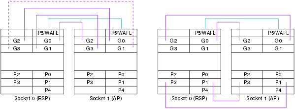
On dual socket (2P) systems the cache coherent xGMI links connect the Data Fabrics of each processor. Socket SP5 processors can use three or four xGMI links depending on bandwidth requirements using the G0-G3 interfaces, or four links between G0, G2, P1, and P3. xGMI links use 16 lanes, unused links release 16 lanes per socket for I/O. As with PCIe links the maximum raw data rate is 32 GT/s. A WAFL link connects the Control Fabrics of each processor, i.e. the PSP, SMUs and other IPs, primarily for temperature monitoring, power and frequency control. Physically they use the PCIe Gen 3 protocol.
Compute Express Links enable cache coherent links to peripheral devices. Type-0 processors are CXL 1.1 compliant and support CXL Type 1 devices (specialized accelerators with no local memory such as a NIC using the CXL.io and CXL.cache protocols) and CXL Type 3 devices (memory expanders, using the CXL.io and CXL.memory protocols) on the P0-P3 interfaces. Up to four CXL Type 1 devices are supported per socket, up to four Type 3 devices per 16-lane interface.
Like its predecessor this socket supports various low speed interfaces. It adds support for the I3C protocol while the LPC interface was deprecated in favor of SPI/ESPI. These busses are generally used to access firmware (PSP ROM and BIOS) i.e. flash memory, and a TPM. Socket SP5 also reserves some pins for audio interfaces, perhaps for future HEDT or workstation processors.
Socket Description[edit]
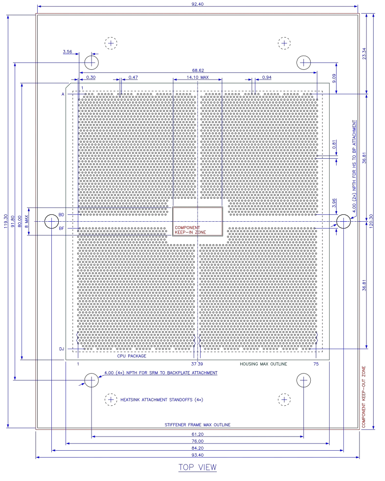
Socket SP5 has a 93.4 mm × 120.3 mm footprint and consists of the following components, from top to bottom:
- Retention Frame
- Rail Frame
- Socket Housing
- Stiffener Frame
- Insulators
- Backplate
Removable components are:
- Heatsink
- Carrier Frame
- External Cap
- PnP Cover Cap
The retention frame, rail frame, and stiffener frame constitute the Socket Retention Mechanism. The heatsink, the CPU in a carrier frame, the SRM, housing, and backplate are separately orderable parts. The latter three are motherboard components for OEMs. Socket SP5 suppliers are Lotes Co. Ltd. (website), Foxconn Interconnect Technology (website), and Amphenol Corp.
LGA sockets use cantilever springs in the socket housing to make electrical contact with flat pads on the bottom of the CPU package. An independent loading mechanism creates the Z-axis compression load between the CPU package and the housing. Considerable force is required to deflect thousands of springs at once which rules out a lever mechanism in favor of screw actuation. The Socket SP5 retention mechanism provides sufficient force to secure the CPU in a mating position, but this socket is actuated by the heatsink, which is attached to the stiffener frame and the backplate. The stiffener frame is likewise attached to the backplate on the bottom side of the motherboard.
The retention frame is a largely flat piece stamped out of stainless steel sheets. It has a window allowing the top of the CPU package lid to protrude for contact with the heatsink. In locked state it applies a load to the flanges on two sides of the lid. The retention frame is attached to the stiffener frame by a hinge which permits vertical motion when the socket is actuated, integrates a stop feature limiting the opening angle, and a torsional spring to keep the frame open while the user inserts or removes the CPU. The retention frame is locked using a single captive screw with a Torx T20 head and M3.5×0.6 or larger thread. It mates with a self-clinching PEM nut on the stiffener frame.
The heatsink is attached using six captive nuts, also with a Torx T20 head. Four of these mate with four 10.0 mm high standoffs with an M3.5×0.6 external thread in the corners of the stiffener frame. These standoffs have conical tips for alignment. Two additional studs with the same threading protude up from the backplate, through openings in the motherboard, insulator sheets, stiffener frame, rail frame, retention frame, and carrier frame, securing the heatsink on the sides of the processor. Backplates with stud heights from 14.40 to 16.00 mm are available to account for different PCB thicknesses. The studs and nuts are symmetrically arranged so the heatsink can be installed 180 degrees rotated. The middle screws are supposed to be tightened first, then diagonally opposed corner screws, with a torque between 12.5 and 15 kgf-cm according to AMD (1.23 to 1.47 N⋅m).
The remaining components have the same function as on Socket SP3. Socket SP5 carrier frames are color coded, the color of frames for EPYC 7004 series processors is TBD.
Feature Summary[edit]
- Lidded land grid array package, 75.4 mm × 72 mm
- 6096 contacts in a 89 × 75 grid, 0.81 mm × 0.94 mm interstitial pitch
- Organic substrate, flip chip die attachment
- 12 × 80 bit DDR5 SDRAM interface
- Eight multi-function I/O interfaces G0-G3, P0-P3
Lane 15 14 13 12 11 10 9 8 7 6 5 4 3 2 1 0 xGMI PCIe / CXL x16 x8 x8 x4 x4 x4 x4 PCIe x2 x2 x2 x2 x2 x2 x2 x2 x1 x1 x1 x1 x1 x1 x1 x1 x1 x1 x1 x1 x1 x1 x1 x1 SATA 17 16 15 14 13 12 11 10 07 06 05 04 03 02 01 00 37 36 35 34 33 32 31 30 27 26 25 24 23 22 21 20 PHY 3 PHY 2 PHY 1 PHY 0
- PCIe Gen 1 to 5 (32 GT/s) protocol supported on all interfaces
- 16 lanes, up to 9 ports per group configurable x16, x8, x4, x2, x1 with power-of-two alignment (e.g. 1x8 + 1x4 + 4x1)
- Max. 8 PCIe ports per interface if any lane is configured as SATA port
- Lane polarity inversion, per port lane reversal
- Up to 128 PCIe lanes total on 1P systems
- Up to 64 or 80 PCIe lanes total per socket on 2P systems
- PCIe Gen 1 to 5 (32 GT/s) protocol supported on all interfaces
- xGMI protocol on G0-G3, P1, and P3, used on 2P systems only
- Four link option 1: G0 (socket 0) ↔ G2 (socket 1), G1 ↔ G3, G2 ↔ G0, G3 ↔ G1
- Four link option 2: G0 ↔ G2, G2 ↔ G0, P1 ↔ P3, P3 ↔ P1
- Three link option: G0 ↔ G2, G1 ↔ G3, G2 ↔ G0
- Max. data rate 32 GT/s
- Lane polarity inversion, x16 lane reversal
- xGMI protocol on G0-G3, P1, and P3, used on 2P systems only
- CXL protocol on the P0-P3 interfaces (Type-0 processors)
- CXL Type 1 (accelerators): One link per interface, 1x16 or 1x8 lanes
- CXL Type 3 (memory expanders): Up to four links per interface, 1x16, 2x8, or 4x4 lanes
- Unused lanes available for PCIe, configurable 1x8, 2x4, or 3x4
- CXL protocol on the P0-P3 interfaces (Type-0 processors)
- SATA Gen 1, 2, 3 (6 Gb/s) protocol on P0 and G3
- P0: SATA00-07 & SATA10-17, G3: SATA20-27 & SATA30-37
- Unused lanes available for PCIe, also lanes sharing a PHY group
- Up to 32 SATA ports total on 1P systems
- Up to 16 SATA ports total per socket on 2P systems (SATA not supported on G3 regardless of xGMI link option)
- SATA Gen 1, 2, 3 (6 Gb/s) protocol on P0 and G3
- Two supplementary I/O interfaces P4, P5
- PCIe Gen 1, 2, 3 (8 GT/s) protocol on both interfaces
- 4 lanes, up to 4 ports per interface configurable x4, x2, x1
- Up to 8 PCIe lanes total on 1P systems
- Up to 6 PCIe lanes total per socket on 2P systems
- WAFL protocol on lane 0-1 of P5, used on 2P systems only
- P5[0] (socket 0) ↔ P5[1] (socket 1)
- PCIe Gen 1, 2, 3 (8 GT/s) protocol on both interfaces
- 4 × USB 1.1, 2.0, 3.2 Gen 1×1 (5 Gb/s)
- Low speed interfaces (some sharing pins):
Processors using Socket SP5[edit]
| Model | Family | Microarch | Core | Cores | Threads | L2$ | L3$ | Base | Turbo | Memory | TDP | Launched | Price | OPN |
|---|---|---|---|---|---|---|---|---|---|---|---|---|---|---|
| 9124 | EPYC | Zen 4 | Genoa | 16 | 32 | 16 MiB 16,384 KiB 16,777,216 B 0.0156 GiB | 64 MiB 65,536 KiB 67,108,864 B 0.0625 GiB | 3 GHz 3,000 MHz 3,000,000 kHz | 3.6 GHz 3,600 MHz 3,600,000 kHz | DDR5-4800 | 200 W 200,000 mW 0.268 hp 0.2 kW | 10 November 2022 | $ 1,083.00 € 974.70 £ 877.23 ¥ 111,906.39 | 100-100000802, 100-100000802WOF |
| 9174F | EPYC | Zen 4 | Genoa | 16 | 32 | 16 MiB 16,384 KiB 16,777,216 B 0.0156 GiB | 256 MiB 262,144 KiB 268,435,456 B 0.25 GiB | 4.1 GHz 4,100 MHz 4,100,000 kHz | 4.15 GHz 4,150 MHz 4,150,000 kHz | DDR5-4800 | 320 W 320,000 mW 0.429 hp 0.32 kW | 10 November 2022 | $ 3,850.00 € 3,465.00 £ 3,118.50 ¥ 397,820.50 | 100-100000796, 100-100000796WOF |
| 9224 | EPYC | Zen 4 | Genoa | 24 | 48 | 24 MiB 24,576 KiB 25,165,824 B 0.0234 GiB | 64 MiB 65,536 KiB 67,108,864 B 0.0625 GiB | 2.5 GHz 2,500 MHz 2,500,000 kHz | 3.65 GHz 3,650 MHz 3,650,000 kHz | DDR5-4800 | 200 W 200,000 mW 0.268 hp 0.2 kW | 10 November 2022 | $ 1,825.00 € 1,642.50 £ 1,478.25 ¥ 188,577.25 | 100-100000939, 100-100000939WOF |
| 9254 | EPYC | Zen 4 | Genoa | 24 | 48 | 24 MiB 24,576 KiB 25,165,824 B 0.0234 GiB | 128 MiB 131,072 KiB 134,217,728 B 0.125 GiB | 2.9 GHz 2,900 MHz 2,900,000 kHz | 3.9 GHz 3,900 MHz 3,900,000 kHz | DDR5-4800 | 200 W 200,000 mW 0.268 hp 0.2 kW | 10 November 2022 | $ 2,299.00 € 2,069.10 £ 1,862.19 ¥ 237,555.67 | 100-100000480, 100-100000480WOF |
| 9274F | EPYC | Zen 4 | Genoa | 24 | 48 | 24 MiB 24,576 KiB 25,165,824 B 0.0234 GiB | 256 MiB 262,144 KiB 268,435,456 B 0.25 GiB | 4.05 GHz 4,050 MHz 4,050,000 kHz | 4.1 GHz 4,100 MHz 4,100,000 kHz | DDR5-4800 | 320 W 320,000 mW 0.429 hp 0.32 kW | 10 November 2022 | $ 3,060.00 € 2,754.00 £ 2,478.60 ¥ 316,189.80 | 100-100000794, 100-100000794WOF |
| 9334 | EPYC | Zen 4 | Genoa | 32 | 64 | 32 MiB 32,768 KiB 33,554,432 B 0.0313 GiB | 128 MiB 131,072 KiB 134,217,728 B 0.125 GiB | 2.7 GHz 2,700 MHz 2,700,000 kHz | 3.85 GHz 3,850 MHz 3,850,000 kHz | DDR5-4800 | 210 W 210,000 mW 0.282 hp 0.21 kW | 10 November 2022 | $ 2,990.00 € 2,691.00 £ 2,421.90 ¥ 308,956.70 | 100-100000800, 100-100000800WOF |
| 9354 | EPYC | Zen 4 | Genoa | 32 | 64 | 32 MiB 32,768 KiB 33,554,432 B 0.0313 GiB | 256 MiB 262,144 KiB 268,435,456 B 0.25 GiB | 3.25 GHz 3,250 MHz 3,250,000 kHz | 3.75 GHz 3,750 MHz 3,750,000 kHz | DDR5-4800 | 280 W 280,000 mW 0.375 hp 0.28 kW | 10 November 2022 | $ 3,420.00 € 3,078.00 £ 2,770.20 ¥ 353,388.60 | 100-100000798, 100-100000798WOF |
| 9354P | EPYC | Zen 4 | Genoa | 32 | 64 | 32 MiB 32,768 KiB 33,554,432 B 0.0313 GiB | 256 MiB 262,144 KiB 268,435,456 B 0.25 GiB | 3.25 GHz 3,250 MHz 3,250,000 kHz | 3.75 GHz 3,750 MHz 3,750,000 kHz | DDR5-4800 | 280 W 280,000 mW 0.375 hp 0.28 kW | 10 November 2022 | $ 2,730.00 € 2,457.00 £ 2,211.30 ¥ 282,090.90 | 100-100000805, 100-100000805WOF |
| 9374F | EPYC | Zen 4 | Genoa | 32 | 64 | 32 MiB 32,768 KiB 33,554,432 B 0.0313 GiB | 256 MiB 262,144 KiB 268,435,456 B 0.25 GiB | 3.85 GHz 3,850 MHz 3,850,000 kHz | 4.1 GHz 4,100 MHz 4,100,000 kHz | DDR5-4800 | 320 W 320,000 mW 0.429 hp 0.32 kW | 10 November 2022 | $ 4,850.00 € 4,365.00 £ 3,928.50 ¥ 501,150.50 | 100-100000792, 100-100000792WOF |
| 9454 | EPYC | Zen 4 | Genoa | 48 | 96 | 48 MiB 49,152 KiB 50,331,648 B 0.0469 GiB | 256 MiB 262,144 KiB 268,435,456 B 0.25 GiB | 2.75 GHz 2,750 MHz 2,750,000 kHz | 3.65 GHz 3,650 MHz 3,650,000 kHz | DDR5-4800 | 290 W 290,000 mW 0.389 hp 0.29 kW | 10 November 2022 | $ 5,225.00 € 4,702.50 £ 4,232.25 ¥ 539,899.25 | 100-100000478, 100-100000478WOF |
| 9454P | EPYC | Zen 4 | Genoa | 48 | 96 | 48 MiB 49,152 KiB 50,331,648 B 0.0469 GiB | 256 MiB 262,144 KiB 268,435,456 B 0.25 GiB | 2.75 GHz 2,750 MHz 2,750,000 kHz | 3.65 GHz 3,650 MHz 3,650,000 kHz | DDR5-4800 | 290 W 290,000 mW 0.389 hp 0.29 kW | 10 November 2022 | $ 4,598.00 € 4,138.20 £ 3,724.38 ¥ 475,111.34 | 100-100000873, 100-100000873WOF |
| 9474F | EPYC | Zen 4 | Genoa | 48 | 96 | 48 MiB 49,152 KiB 50,331,648 B 0.0469 GiB | 256 MiB 262,144 KiB 268,435,456 B 0.25 GiB | 3.6 GHz 3,600 MHz 3,600,000 kHz | 3.95 GHz 3,950 MHz 3,950,000 kHz | DDR5-4800 | 360 W 360,000 mW 0.483 hp 0.36 kW | 10 November 2022 | $ 6,780.00 € 6,102.00 £ 5,491.80 ¥ 700,577.40 | 100-100000788, 100-100000788WOF |
| 9534 | EPYC | Zen 4 | Genoa | 64 | 128 | 64 MiB 65,536 KiB 67,108,864 B 0.0625 GiB | 256 MiB 262,144 KiB 268,435,456 B 0.25 GiB | 2.45 GHz 2,450 MHz 2,450,000 kHz | 3.55 GHz 3,550 MHz 3,550,000 kHz | DDR5-4800 | 280 W 280,000 mW 0.375 hp 0.28 kW | 10 November 2022 | $ 8,803.00 € 7,922.70 £ 7,130.43 ¥ 909,613.99 | 100-100000799, 100-100000799WOF |
| 9554 | EPYC | Zen 4 | Genoa | 64 | 128 | 64 MiB 65,536 KiB 67,108,864 B 0.0625 GiB | 256 MiB 262,144 KiB 268,435,456 B 0.25 GiB | 3.1 GHz 3,100 MHz 3,100,000 kHz | 3.75 GHz 3,750 MHz 3,750,000 kHz | DDR5-4800 | 360 W 360,000 mW 0.483 hp 0.36 kW | 10 November 2022 | $ 9,087.00 € 8,178.30 £ 7,360.47 ¥ 938,959.71 | 100-100000790, 100-100000790WOF |
| 9554P | EPYC | Zen 4 | Genoa | 64 | 128 | 64 MiB 65,536 KiB 67,108,864 B 0.0625 GiB | 256 MiB 262,144 KiB 268,435,456 B 0.25 GiB | 3.1 GHz 3,100 MHz 3,100,000 kHz | 3.75 GHz 3,750 MHz 3,750,000 kHz | DDR5-4800 | 360 W 360,000 mW 0.483 hp 0.36 kW | 10 November 2022 | $ 7,104.00 € 6,393.60 £ 5,754.24 ¥ 734,056.32 | 100-100000804, 100-100000804WOF |
| 9634 | EPYC | Zen 4 | Genoa | 84 | 168 | 84 MiB 86,016 KiB 88,080,384 B 0.082 GiB | 384 MiB 393,216 KiB 402,653,184 B 0.375 GiB | 2.25 GHz 2,250 MHz 2,250,000 kHz | 3.1 GHz 3,100 MHz 3,100,000 kHz | DDR5-4800 | 290 W 290,000 mW 0.389 hp 0.29 kW | 10 November 2022 | $ 10,304.00 € 9,273.60 £ 8,346.24 ¥ 1,064,712.32 | 100-100000797, 100-100000797WOF |
| 9654 | EPYC | Zen 4 | Genoa | 96 | 192 | 96 MiB 98,304 KiB 100,663,296 B 0.0938 GiB | 384 MiB 393,216 KiB 402,653,184 B 0.375 GiB | 2.4 GHz 2,400 MHz 2,400,000 kHz | 3.55 GHz 3,550 MHz 3,550,000 kHz | DDR5-4800 | 360 W 360,000 mW 0.483 hp 0.36 kW | 10 November 2022 | $ 11,805.00 € 10,624.50 £ 9,562.05 ¥ 1,219,810.65 | 100-100000789, 100-100000789WOF |
| 9654P | EPYC | Zen 4 | Genoa | 96 | 192 | 96 MiB 98,304 KiB 100,663,296 B 0.0938 GiB | 384 MiB 393,216 KiB 402,653,184 B 0.375 GiB | 2.4 GHz 2,400 MHz 2,400,000 kHz | 3.55 GHz 3,550 MHz 3,550,000 kHz | DDR5-4800 | 360 W 360,000 mW 0.483 hp 0.36 kW | 10 November 2022 | $ 10,625.00 € 9,562.50 £ 8,606.25 ¥ 1,097,881.25 | 100-100000803, 100-100000803WOF |
| Count: 18 |
Photos[edit]
| This section is empty; you can help add the missing info by editing this page. |
Package Diagrams[edit]
SP5 package. All dimensions in millimeters.
SP5 carrier frame. All dimensions in millimeters.
Socket Diagrams[edit]
Socket SP5 housing (AMD). All dimensions in millimeters.
PCB layout of Socket SP5. All dimensions in millimeters.
Pin Map[edit]
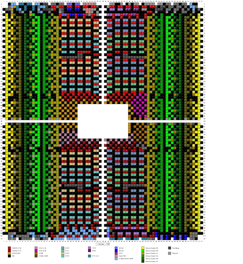
Socket SP5 pinout, top view. This is a preview, click for a larger image and other views.
Pin Description[edit]
| Signal | Type | Description | ||||||||||
|---|---|---|---|---|---|---|---|---|---|---|---|---|
| MA-ML_ALERT_L | I-IOMEM-S | DRAM Channel A-L ALERT for CRC Error | ||||||||||
| MA-ML_RESET_L | O-IOMEM-S | DRAM Channel A-L DIMM Reset | ||||||||||
| MA0-ML0_CLK_H/L MA1-ML1_CLK_H/L |
O-IOMEM-D | DRAM Channel A-L DIMM 0/1 Differential Clock | ||||||||||
| MAA-MLA_CA[6:0] | O-IOMEM-S | DRAM Channel A-L Subchannel A Command/Address Bus | ||||||||||
| MAB-MLB_CA[6:0] | O-IOMEM-S | DRAM Channel A-L Subchannel B Command/Address Bus | ||||||||||
| MAA-MLA_CHECK[7:0] | B-IOMEM-S | DRAM Channel A-L Subchannel A ECC Check Byte | ||||||||||
| MAB-MLB_CHECK[7:0] | B-IOMEM-S | DRAM Channel A-L Subchannel B ECC Check Byte | ||||||||||
| MAA-MLA_DATA[31:0] | B-IOMEM-S | DRAM Channel A-L Subchannel A Data Bus | ||||||||||
| MAB-MLB_DATA[31:0] | B-IOMEM-S | DRAM Channel A-L Subchannel B Data Bus | ||||||||||
| MAA-MLA_DQS_H/L[9:0] | B-IOMEM-D | DRAM Channel A-L Subchannel A Data Strobes (x4 and x8) Differential Pair | ||||||||||
| MAB-MLB_DQS_H/L[9:0] | B-IOMEM-D | DRAM Channel A-L Subchannel B Data Strobes (x4 and x8) Differential Pair | ||||||||||
| MAA-MLA_PAR | O-IOMEM-S | DRAM Channel A-L Subchannel A Parity | ||||||||||
| MAB-MLB_PAR | O-IOMEM-S | DRAM Channel A-L Subchannel B Parity | ||||||||||
| MAA0-MLA0_CS_L[1:0] MAA1-MLA1_CS_L[1:0] |
O-IOMEM-S | DRAM Channel A-L DIMM 0/1 Subchannel A Chip Select | ||||||||||
| MAB0-MLB0_CS_L[1:0] MAB1-MLB1_CS_L[1:0] |
O-IOMEM-S | DRAM Channel A-L DIMM 0/1 Subchannel B Chip Select | ||||||||||
| MAA0-MLA0_RSP_L MAA1-MLA1_RSP_L |
I-IOMEM-S | DRAM Channel A-L DIMM 0/1 Subchannel A Response Signal | ||||||||||
| MAB0-MLB0_RSP_L MAB1-MLB1_RSP_L |
I-IOMEM-S | DRAM Channel A-L DIMM 0/1 Subchannel B Response Signal | ||||||||||
| FORCE_SELFREFRESH | I-IO18S5-S | NVDIMM Force Self-Refresh | ||||||||||
| NV_SAVE_L | O-IO18S5-S | NVDIMM SAVE Signal | ||||||||||
| P0/P2_RXP/RXN[15:0] | I-PCIE-D | PCIe Receive Data Differential Pairs | ||||||||||
| P0/P2_TXP/TXN[15:0] | O-PCIE-D | PCIe Transmit Data Differential Pairs | ||||||||||
| P1/P3_RXP/RXN[15:0] | I-XGMI-D or I-PCIE-D | xGMI or PCIe Receive Data Differential Pairs | ||||||||||
| P1/P3_TXP/TXN[15:0] | O-XGMI-D or O-PCIE-D | xGMI or PCIe Transmit Data Differential Pairs | ||||||||||
| P4/P5_RXP/RXN[3:0] | I-PCIE-D | PCIe Receive Data Differential Pairs | ||||||||||
| P4/P5_TXP/TXN[3:0] | O-PCIE-D | PCIe Transmit Data Differential Pairs | ||||||||||
| G0-G3_RXP/RXN[15:0] | I-XGMI-D or I-PCIE-D | xGMI or PCIe Receive Data Differential Pairs | ||||||||||
| G0-G3_TXP/TXN[15:0] | I-XGMI-D or O-PCIE-D | xGMI or PCIe Transmit Data Differential Pairs | ||||||||||
| PCIE_RST0/1_L | O-IO18S5-S | PCIe Reset Signals from I/O Die | ||||||||||
| WAFL_RXP/RXN[1:0] | I-WAFL-D | WAFL Receive Data Differential Pairs (alt. func. of P5[1:0]) | ||||||||||
| WAFL_TXP/TXN[1:0] | O-WAFL-D | WAFL Transmit Data Differential Pairs | ||||||||||
| SATA(0-3)(0-7)_RXP/RXN | I-SATA-D | SATA Receive Data Differential Pairs (alt. func. of P0 & G3) | ||||||||||
| SATA(0-3)(0-7)_TXP/TXN | O-SATA-D | SATA Transmit Data Differential Pairs | ||||||||||
| DEVSLP(0-1) | O-IO18S5-OD | SATA DEVSLP | ||||||||||
| SATA_ACT_L | O-IO18S5-OD | SATA Activity signal (HD LED) | ||||||||||
| SATA_ZP(0-1)_L | O-IO18S5-OD | Zero Power SATA ODD | ||||||||||
| SGPIO(0-3)_CLK | O-IO18S5-S | SGPIO CLK Output for SATA ports 0x-3x | ||||||||||
| SGPIO_DATAOUT | O-IO18S5-S | SGPIO DATA Output for all SATA ports | ||||||||||
| SGPIO_LOAD | O-IO18S5-S | SGPIO LOAD Output for all SATA ports | ||||||||||
| USB(0-1)(0-1)_DP/DN | B-USB2_S5-D | USB High Speed I/O Differential Pairs | ||||||||||
| USB(0-1)(0-1)_RXP/RXN | I-USB3_S5-D | USB Super Speed Receive Differential Pairs | ||||||||||
| USB(0-1)(0-1)_TXP/TXN | O-USB3_S5-D | USB Super Speed Transmit Differential Pairs | ||||||||||
| USB(0-1)(0-1)_OC_L | I-IO18S5-S | USB Over Current signal from USB connector | ||||||||||
| UART0_CTS_L | I-IO18S5-S | UART0 Clear To Send Input (alt. func. of UART2_TXD) | ||||||||||
| UART0_INTR | I-IO18S5-S | UART0 Interrupt Request | ||||||||||
| UART0_RTS_L | O-IO18S5-S | UART0 Request To Send Output (alt. func. of UART2_RXD) | ||||||||||
| UART(0-2)_RXD | I-IO18S5-S | UART Receive Data | ||||||||||
| UART(0-2)_TXD | O-IO18S5-S | UART Transmit Data | ||||||||||
| SPI_CLK(0-1) | O-IO18S5-S | SPI Clock | ||||||||||
| SPI(0-1)_DAT[0] | B-IO18S5-S or O-IO18S5-S | SPI Data 0 for multi-I/O device or Data Out | ||||||||||
| SPI(0-1)_DAT[1] | B-IO18S5-S or I-IO18S5-S | SPI Data 1 for multi-I/O device or Data In | ||||||||||
| SPI(0-1)_DAT[3:2] | B-IO18S5-S | SPI Port Data 2, 3 for multi-I/O device | ||||||||||
| SPI_CS(0-2)_L | O-IO18S5-S | SPI Chip Select | ||||||||||
| SPI_TPM_CS_L | O-IO18S5-S | SPI Chip Select for TPM | ||||||||||
| ESPI_CLK(0-2) | O-IO18S5-S | ESPI Clock (0-1 alt. func. of SPI_CLK0, SPI_CLK1) | ||||||||||
| ESPI(0-1)_DAT[3:0] | B-IO18S5-S | ESPI Data (alt. func. of SPI(0-1)_DAT[3:0]) | ||||||||||
| ESPI_CS(0-1)_L | O-IO18S5-S | ESPI Chip Select | ||||||||||
| ESPI(0-1)_ALERT_L | I-IO18S5-S | ESPI Alert | ||||||||||
| ESPI_RSTIN_L | I-IO18S5-S | ESPI Reset Input | ||||||||||
| ESPI_RSTOUT_L | O-IO18S5-S | ESPI Reset Output | ||||||||||
| I3C(0-3)_SCL | O-IO11S3-S | I3C Clock | ||||||||||
| I3C(0-3)_SDA | B-IO11S3-S | I3C Data | ||||||||||
| I2C(0-3)_SCL | B-IO18S5-OD | I2C Clock (alt. func. of I3C0-I3C3) | ||||||||||
| I2C(0-3)_SDA | B-IO18S5-OD | I2C Data | ||||||||||
| I2C(4-5)_SCL | B-IO18S5-OD | I2C Clock | ||||||||||
| I2C(4-5)_SDA | B-IO18S5-OD | I2C Data | ||||||||||
| SEC_SCL | I-IO11S3-S | I3C or I2C CLK for security function | ||||||||||
| SEC_SDA | B-IO11S3-S | I3C or I2C Data for security function | ||||||||||
| SPD(0-3)_SCL, SPD(0-3)_SDA | SPD Busses (I3C0-I3C3) | |||||||||||
| SPD_HOST_CTRL_L | O-IO18S5-OD | SPD I3C/I2C Bus Mux Control Signal | ||||||||||
| UBM_SCL, UBM_SDA | UBM Bus (I2C4) | |||||||||||
| UBM_CPRSNT_CHANGE_DET_L | I-IO18S5-S | UBM Subsystem Interrupt | ||||||||||
| SMBUS(0-1)_SCL | B-IO11S3-OD | SMBUS Clock (alt. func. of I2C3/I2C5) | ||||||||||
| SMBUS(0-1)_SDA | B-IO11S3-OD | SMBUS Data | ||||||||||
| HP_SCL, HP_SDA | Hotplug SMBUS (I2C4) | |||||||||||
| BMC_SCL, BMC_SDA | BMC SMBUS (I2C5/SMBUS1) | |||||||||||
| AGPIO* | Advanced GPIO pin for interrupt, wake, or I/O | |||||||||||
| GENINT_L | I-IO18S5-S | Generic Interrupt Request | ||||||||||
| REFCLK100SSC_P/N | O-CLK-D | 100 MHz CPU Reference Clock Output from BSP for AP | ||||||||||
| GPP_CLK10P/N | I-CLK-D | 100 MHz CPU Reference Clock Input for AP from BSP | ||||||||||
| GPP_CLK(0-1)(1-5)P/N | O-CLK-D | 100 MHz Differential PCIe Reference Clock Outputs from I/O Die (Internal CLKGEN Mode) | ||||||||||
| GPP_CLK(0-1)2P/N | I-CLK-D | 100 MHz Differential PCIe Reference Clock Input (External CLKGEN Mode) | ||||||||||
| X32K_X1/X2 | A | 32768 Hz Real Time Clock XTAL | ||||||||||
| X48M_X1/X2 | A or I-IO18S5-S | 48 MHz clock XTAL or (X48M_X1 only): 48 MHz reference clock input for the integrated clock generator | ||||||||||
| RTCCLK | O-IO18S5-S | 32768 Hz Real Time Clock output, e.g. BSP to AP, or for a device requiring an RTC clock | ||||||||||
| KBRST_L | I-IO18S5-S | Keyboard Controller Reset Input (warm reset) | ||||||||||
| PM_INTR_L | I-IO18S5-S | Hotplug SMBus Subsystem Interrupt Input for NVMe Drives and Hotplug Slots | ||||||||||
| PWR_BTN_L | I-IO18S5-S | Power Button; Requests sleep state or causes wake event | ||||||||||
| PWR_GOOD | I-IO18S5-S | Power Good Input; Asserted when all voltages are within specification; From motherboard to BSP or BSP to AP | ||||||||||
| PWRGD_OUT | O-IO18S5-S | Power Good Output, from BSP to PWR_GOOD input of AP | ||||||||||
| RESET_L | B-IO18S5-OD | Bidirectional signal that resets the processor when asserted; Normally controlled by an internal state machine but can also be asserted by a second external source, in a 2P system from BSP to AP | ||||||||||
| RSMRST_L | I-IO18S5-S | Resume Reset from motherboard, resets all in-processor S5 and S0 logic; Asserted on power up, deasserted when S5 power supplies are within specification | ||||||||||
| SLP_S3/S5_L | O-IO18S5-S | S3/S5 Sleep State Power Plane Control Signal | ||||||||||
| SYS_RESET_L | I-IO18S5-S | System Reset Input (reset button) | ||||||||||
| WAKE_L | B-IO18S5-OD | PCIe WAKE_L signal, wake system out of sleep state | ||||||||||
| NMI_SYNC_FLOOD_L | I-IO33-S | Signals a NMI or a Sync Flood indicating a fatal system error | ||||||||||
| ALERT_L | O-IO18S5-OD | SB-TSI Interrupt or APML Alert Signal | ||||||||||
| PROCHOT_L | I-IO18S5-S | Asserted to force the processor into HTC-active state | ||||||||||
| SIC | I-IO11S3-S | Sideband Interface Clock[1] | ||||||||||
| SID | B-IO11S3-S | Sideband Interface Data | ||||||||||
| THERMTRIP_L | O-IO18S5-OD | Temperature Trip Output | ||||||||||
| BP(0-3) | B-IO18S5-S | Break Point Indicator; Used to trigger external test equipment such as oscilloscopes and logic analyzers | ||||||||||
| DBREQ_L | I-IO18S5-S | Debug Request input to JTAG controller | ||||||||||
| TCK | I-IO18S5-S | JTAG Clock | ||||||||||
| TDI | I-IO18S5-S | JTAG Data Input | ||||||||||
| TDO | O-IO18S5-S | JTAG Data Output | ||||||||||
| TMS | I-IO18S5-S | JTAG Mode Select | ||||||||||
| TRST_L | I-IO18S5-S | JTAG Reset | ||||||||||
| TEST* | Test/Debug signals | |||||||||||
| XTRIG_L[7:4] | B-IO18S5-OD | XTRIG Debug Signals | ||||||||||
| PCC0_L/PCC1_L | I-IO18S5-S | |||||||||||
| SVC0, SVC1 | Serial VID Bus 0/1 Clock; Bus 0: VDDCR_CPU0, VDDCR_SOC; Bus 1: VDDCR_CPU1; VDDIO regulator supported by both busses | |||||||||||
| SVD0, SVD1 | Serial VID Bus 0/1 Data | |||||||||||
| SVT0, SVT1 | Serial VID Bus 0/1 Telemetry Output | |||||||||||
| VDDBT_RTC_G | Integrated Real Time Clock battery power supply | |||||||||||
| RTC_LDO_SELECT | Enables the LDO integrated in Socket SP5 processors so VDDBT_RTC_G can be sourced directly from a 3 V coin-cell battery | |||||||||||
| VDDCR_CPU0 | S | Core Power Supply 0 | ||||||||||
| VDDCR_CPU0_SENSE | Differential (with VSS_SENSE_A) feedback for VDDCR_CPU0 power supply | |||||||||||
| VDDCR_CPU1 | S | Core Power Supply 1 | ||||||||||
| VDDCR_CPU1_SENSE | Differential (with VSS_SENSE_C) feedback for VDDCR_CPU1 power supply | |||||||||||
| VDDCR_SOC | S | Power Supply for Digital Logic | ||||||||||
| VDDCR_SOC_SENSE | Differential (with VSS_SENSE_A) feedback for VDDCR_SOC power supply | |||||||||||
| VDDIO | S | Power Supply for Caches and PHY Macros | ||||||||||
| VDDIO_SENSE | Differential (with VSS_SENSE_B) feedback for VDDIO power supply | |||||||||||
| VDDIO_AUDIO | S | To be connected to VDD_18_S5 supply | ||||||||||
| VDD_11_S3 | S | 1.1 V DDR5 I/O Power Supply | ||||||||||
| VDD_11_S3_SENSE | Differential (with VSS_SENSE_C) feedback for VDD_11_S3 power supply | |||||||||||
| VDD_18_S5 | S | 1.8 V Supply for Analog Circuits and GPIOs | ||||||||||
| VDD_18_S5_SENSE | Differential (with VSS_SENSE_D) feedback for VDD_18_S5 power supply | |||||||||||
| VDD_33_S5 | S | 3.3 V I/O Supply Voltage | ||||||||||
| VDD_33_S5_SENSE | Differential (with VSS_SENSE_B) feedback for VDD_33_S5 power supply | |||||||||||
| VSS | S | Ground for all power supplies | ||||||||||
| VSS_SENSE_A/B/C/D | S | VSS SENSE Feedback Signal to voltage regulators | ||||||||||
| AZ_*, SW_* | Reserved Signals (Azalia HDA, SoundWire) | |||||||||||
| CORETYPE(0-2) | Processor Core Type Indicator; NC = Not connected, VSS = connected to VSS on the package
| |||||||||||
| CPU_PRESENT_L | CPU Presence Indicator, connected to VSS on the package | |||||||||||
| SP5R1-SP5R4 | Processor Family Revision Identifier; NC = Not connected, VSS = connected to VSS on the package
| |||||||||||
| SA[1:0] | I-IO18S5-S | Socket Identifier; 0 = connected to VSS, 1 = 2.2 kΩ PU to VDD_18_S5
| ||||||||||
| RSVD | Reserved |
- ↑ The Sideband Interface (SBI) a.k.a. APML is a SMBus interconnect to the processor's SB-RMI and SB-TSI interfaces.
Pin Types[edit]
| Voltage Domain Internal to SoC, derived from VDDIO | |
|---|---|
| I/O-xGMI/PCIE/SATA/WAFL-D | Input / Output, xGMI / PCIe / SATA / WAFL Domain, Differential |
| Voltage Domain Internal to SoC, derived from VDD_18_S5 | |
| I/O-USB3_S5-D | Input / Output, USB3, Differential |
| I/O-CLK-D | Input / Output, CLK, Differential |
| Other Voltage Domains | |
| I/O/B-IOMEM-S | Input / Output / Bidirectional, VDD_11_S3, Single-Ended |
| O/B-IOMEM-D | Output / Bidirectional, VDD_11_S3, Differential |
| I/O/B-IO18S5-S | Input / Output / Bidirectional, VDD_18_S5, Single-Ended |
| O/B-IO18S5-OD | Output / Bidirectional, VDD_18_S5, Open Drain |
| B-USB2_S5-D | Bidirectional, VDD_33_S5 USB2, Differential |
| A | Analog |
| S | Supply Voltage |
Bibliography[edit]
See also[edit]
| designer | AMD + |
| first launched | November 10, 2022 + |
| instance of | package + |
| market segment | Server + |
| microarchitecture | Zen 4 + |
| name | Socket SP5 + |
| package | SP5 + and FCLGA-6096 + |
| package contacts | 6,096 + |
| package length | 75.4 mm (7.54 cm, 2.969 in) + |
| package pitch | 0.81 mm (0.0319 in) + and 0.94 mm (0.037 in) + |
| package type | FC-OLGA + |
| package width | 72 mm (7.2 cm, 2.835 in) + |
| socket | Socket SP5 + |
| tdp | 400 W (400,000 mW, 0.536 hp, 0.4 kW) + |
