| Edit Values | |
| Package SP4 | |
| General Info | |
| Designer | AMD |
| Introduction | February 21, 2018 (launched) |
| Market | Embedded |
| Microarchitecture | Zen |
| TDP | 100 W 100,000 mW 0.134 hp 0.1 kW |
| Package | |
| Name | BGA-2028 |
| Type | FC-OBGA |
| Contacts | 2028 |
| Dimension | 45 mm 4.5 cm × 45 mm1.772 in 4.5 cm 1.772 in |
| Pitch | 0.8 mm 0.0315 in |
| Contemporary | |
| SP4r2 | |
SP4 and its contemporary SP4r2 are microprocessor packages of AMD EPYC 3000 "Snowy Owl" embedded processors.
- Server processors of the same generation (EPYC 7001) use Socket SP3.
Contents
Overview[edit]
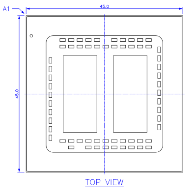
SP4 is a ball grid array package with 0.8 mm non-uniform pitch, 45 mm × 45 mm in size, with flip chip die attachment and a stiffener frame. The processors using these packages are members of AMD's x86 CPU Family 17h with CPU cores based on the Zen microarchitecture, and are fabricated on a GlobalFoundries 14 nm process.
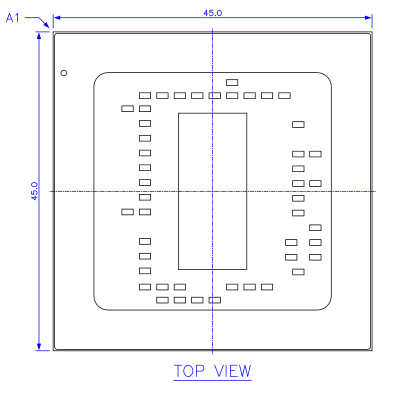
SP4 is a multi-chip package with two identical "Zeppelin" ZP-B2 dies. AMD used the same dies in various revisions for EPYC 7001 server and embedded processors, first generation Ryzen Threadripper HEDT and Ryzen desktop processors; see CPU Family 17h. The pin compatible SP4r2 package carries one of these dies. They integrate eight CPU cores, two memory controllers, two 16-lane multi-function I/O interfaces and other I/O facilities. Both package types are intended for single processor systems so xGMI links are not supported. As on Ryzen Threadripper 1900 processors two GMI links connect the dies of the SP4 package. The multi-function I/O interfaces can be configured as PCIe, SATA, SATA Express, or XGBE links. The latter support the 10GBASE-KR, 1000BASE-KX, and SGMII (10/100/1000 Mbit/s) backplane Ethernet protocols.
Features[edit]
- Lidless ball grid array package with stiffener frame, 45 mm × 45 mm
- 2028 contacts, 0.8 mm non-uniform pitch
- Organic substrate, flip chip die attachment
- 4 × 72 bit DDR4 SDRAM interface
- Four multi-function I/O interfaces P0, P1, G0, G1
Lane 15 14 13 12 11 10 9 8 7 6 5 4 3 2 1 0 PCIe x16 x8 x8 x4 x4 x4 x4 x2 x2 x2 x2 x2 x2 x2 x2 x1 x1 x1 x1 x1 x1 x1 x1 x1 x1 x1 x1 x1 x1 x1 x1 SATAe 1 0 SATA 7 6 5 4 3 2 1 0 XGBE 3 2 1 0 PHY 4 PHY 3 PHY 2 PHY 1 PHY 0
- PCIe Gen 1, 2, 3 (8 GT/s) protocol supported on all interfaces
- 16 lanes, up to 8 ports per interface configurable x16, x8, x4, x2, x1 with power-of-two alignment (e.g. 1x4 + 4x1 + 1x8)
- Max. 7 PCIe ports in each 8-lane subset (e.g. 0x8 + 8x1 is not possible)
- Max. 7 PCIe ports per interface if any lane is configured as SATA port
- Different PCIe generations supported on the ports in the same interface
- Lane polarity inversion, per port lane reversal
- Up to 64 PCIe lanes total
- PCIe Gen 1, 2, 3 (8 GT/s) protocol supported on all interfaces
- SATA Express supported on the lowest four lanes of P0 and G1
- Combines PCIe and SATA controllers on the same two lanes with a GPIO pin for a device to indicate its controller type
- P0: SATAE00, SATAE01; G1: SATAE10, SATAE11
- Up to 4 ports total
- SATA Express supported on the lowest four lanes of P0 and G1
- SATA Gen 1, 2, 3 (6 Gb/s) protocol supported on the lower 8 lanes of P0 and G1
- P0: SATA00-07, G1: SATA10-17
- Up to 16 ports total
- SATA Gen 1, 2, 3 (6 Gb/s) protocol supported on the lower 8 lanes of P0 and G1
- XGBE protocols supported on lanes 4-7 of P0 and G1
- P0: XGBE00-03, G1: XGBE10-13
- Up to 8 ports total
- XGBE protocols supported on lanes 4-7 of P0 and G1
- Five PHY groups on each interface
- Lanes sharing a PHY group must use the same protocol (PCIe, SATA, XGBE)
- Five PHY groups on each interface
- 4 × USB 1.1, 2.0, 3.1 Gen 1 (5 Gb/s) ports
Processors using package SP4[edit]
| Model | Cores | Threads | L2$ | L3$ | Base Frequ. | Turbo one core | Memory (1DPC) | Memory channels | Tjmin | Tjmax | cTDP↓ | TDP | Launched | Price | LTB | OPN |
|---|---|---|---|---|---|---|---|---|---|---|---|---|---|---|---|---|
| 3301 | 12 | 12 | 6 MiB 6,144 KiB 6,291,456 B 0.00586 GiB | 32 MiB 32,768 KiB 33,554,432 B 0.0313 GiB | 2 GHz 2,000 MHz 2,000,000 kHz | 3 GHz 3,000 MHz 3,000,000 kHz | DDR4-2666 | 4 | 0 °C 273.15 K 32 °F 491.67 °R | 95 °C 368.15 K 203 °F 662.67 °R | 65 W 65,000 mW 0.0872 hp 0.065 kW | 21 February 2018 | $ 450.00 € 405.00 £ 364.50 ¥ 46,498.50 | |||
| 3351 | 12 | 24 | 6 MiB 6,144 KiB 6,291,456 B 0.00586 GiB | 32 MiB 32,768 KiB 33,554,432 B 0.0313 GiB | 1.9 GHz 1,900 MHz 1,900,000 kHz | 3 GHz 3,000 MHz 3,000,000 kHz | DDR4-2666 | 4 | 0 °C 273.15 K 32 °F 491.67 °R | 105 °C 378.15 K 221 °F 680.67 °R | 60 W 60,000 mW 0.0805 hp 0.06 kW | 80 W 80,000 mW 0.107 hp 0.08 kW | 21 February 2018 | 2028 | PE3351BNQCAAF | |
| 3401 | 16 | 16 | 8 MiB 8,192 KiB 8,388,608 B 0.00781 GiB | 32 MiB 32,768 KiB 33,554,432 B 0.0313 GiB | 1.85 GHz 1,850 MHz 1,850,000 kHz | 3 GHz 3,000 MHz 3,000,000 kHz | DDR4-2666 | 4 | 0 °C 273.15 K 32 °F 491.67 °R | 105 °C 378.15 K 221 °F 680.67 °R | 85 W 85,000 mW 0.114 hp 0.085 kW | 21 February 2018 | ||||
| 3451 | 16 | 32 | 8 MiB 8,192 KiB 8,388,608 B 0.00781 GiB | 32 MiB 32,768 KiB 33,554,432 B 0.0313 GiB | 2.15 GHz 2,150 MHz 2,150,000 kHz | 3 GHz 3,000 MHz 3,000,000 kHz | DDR4-2666 | 4 | 0 °C 273.15 K 32 °F 491.67 °R | 105 °C 378.15 K 221 °F 680.67 °R | 80 W 80,000 mW 0.107 hp 0.08 kW | 100 W 100,000 mW 0.134 hp 0.1 kW | 21 February 2018 | $ 880.00 € 792.00 £ 712.80 ¥ 90,930.40 | 2028 | PE3451BMQGAAF |
| Count: 4 |
Photos[edit]
| This section is empty; you can help add the missing info by editing this page. |
Package Diagrams[edit]
 SP4 package |
 SP4r2 package |
Pin Map[edit]
| This section is empty; you can help add the missing info by editing this page. |
Bibliography[edit]
- "Product Brief: AMD EPYC™ Embedded 3000 Family", AMD Publ. #1887102, 2018
- "Product Brief: AMD EPYC™ Embedded 3000 Family", AMD Publ. #1887102, Rev. E, 2019
- "Processor Programming Reference (PPR) for AMD Family 17h Model 01h, Revision B1 Processors", AMD Publ. #54945, Rev. 1.14, April 15, 2017
- "Processor Programming Reference (PPR) for AMD Family 17h Model 01h, Revision B1 Processors", AMD Publ. #54945, Rev. 3.00, April 14, 2019
- "Revision Guide for AMD Family 17h Models 00h-0Fh Processors", AMD Publ. #55449, Rev. 1.19, December 2019
- "Embedded Processor Specifications". AMD.com.
See also[edit]
| designer | AMD + |
| first launched | February 21, 2018 + |
| instance of | package + |
| market segment | Embedded + |
| microarchitecture | Zen + |
| name | Package SP4 + |
| package | BGA-2028 + |
| package contacts | 2,028 + |
| package length | 45 mm (4.5 cm, 1.772 in) + |
| package pitch | 0.8 mm (0.0315 in) + |
| package type | FC-OBGA + |
| package width | 45 mm (4.5 cm, 1.772 in) + |
| tdp | 100 W (100,000 mW, 0.134 hp, 0.1 kW) + |