Semiconductor & Computer Engineering
(added server platform) |
(→Individual Core) |
||
| (101 intermediate revisions by 19 users not shown) | |||
| Line 26: | Line 26: | ||
|stages min=14 | |stages min=14 | ||
|stages max=19 | |stages max=19 | ||
| − | |isa | + | |isa=x86-64 |
| − | |||
| − | |||
|extension=MOVBE | |extension=MOVBE | ||
|extension 2=MMX | |extension 2=MMX | ||
| Line 73: | Line 71: | ||
|l3 desc=11-way set associative | |l3 desc=11-way set associative | ||
|core name=Skylake X | |core name=Skylake X | ||
| − | |core name 2=Skylake SP | + | |core name 2=Skylake W |
| + | |core name 3=Skylake SP | ||
|predecessor=Broadwell | |predecessor=Broadwell | ||
|predecessor link=intel/microarchitectures/broadwell | |predecessor link=intel/microarchitectures/broadwell | ||
| + | |successor=Cascade Lake | ||
| + | |successor link=intel/microarchitectures/cascade lake | ||
| + | |contemporary=Skylake (client) | ||
| + | |contemporary link=intel/microarchitectures/skylake (client) | ||
|pipeline=Yes | |pipeline=Yes | ||
|OoOE=Yes | |OoOE=Yes | ||
| Line 91: | Line 94: | ||
{| class="wikitable" | {| class="wikitable" | ||
|- | |- | ||
| − | ! Core !! Abbrev !! Target | + | ! Core !! Abbrev !! Platform !! Target |
|- | |- | ||
| − | | {{intel|Skylake | + | | {{intel|Skylake SP|l=core}} || SKL-SP || {{intel|Purley|l=platform}} || Server Scalable Processors |
|- | |- | ||
| − | | {{intel|Skylake | + | | {{intel|Skylake X|l=core}} || SKL-X || {{intel|Basin Falls|l=platform}} || High-end desktops & enthusiasts market |
| + | |- | ||
| + | | {{intel|Skylake W|l=core}} || SKL-W || {{intel|Basin Falls|l=platform}} || Enterprise/Business workstations | ||
| + | |- | ||
| + | | {{intel|Skylake DE|l=core}} || SKL-DE || || Dense server/edge computing | ||
|} | |} | ||
| Line 116: | Line 123: | ||
|- | |- | ||
! Cores !! {{intel|Hyper-Threading|HT}} !! {{intel|Turbo Boost|TBT}} !! {{x86|AVX-512}} !! AVX-512 Units !! {{intel|Ultra Path Interconnect|UPI}} links !! Scalability | ! Cores !! {{intel|Hyper-Threading|HT}} !! {{intel|Turbo Boost|TBT}} !! {{x86|AVX-512}} !! AVX-512 Units !! {{intel|Ultra Path Interconnect|UPI}} links !! Scalability | ||
| + | |- | ||
| + | | [[File:xeon logo (2015).png|50px|link=intel/xeon d]] || {{intel|Xeon D}} || style="text-align: left;" | Dense servers / edge computing || [[4 cores|4]]-[[18 cores|18]] || {{tchk|yes}} || {{tchk|yes}} || {{tchk|yes}} || 1 || colspan="2" {{tchk|no}} | ||
| + | |- | ||
| + | | [[File:xeon logo (2015).png|50px|link=intel/xeon w]] || {{intel|Xeon W}} || style="text-align: left;" | Business workstations || [[4 cores|4]]-[[18 cores|18]] || {{tchk|yes}} || {{tchk|yes}} || {{tchk|yes}} || 2 || colspan="2" {{tchk|no}} | ||
|- | |- | ||
| [[File:xeon bronze (2017).png|50px]] || {{intel|Xeon Bronze}} || style="text-align: left;" | Entry-level performance / <br>Cost-sensitive || [[6 cores|6]] - [[8 cores|8]] || {{tchk|no}} || {{tchk|no}} || {{tchk|yes}} || 1 || 2 || Up to 2 | | [[File:xeon bronze (2017).png|50px]] || {{intel|Xeon Bronze}} || style="text-align: left;" | Entry-level performance / <br>Cost-sensitive || [[6 cores|6]] - [[8 cores|8]] || {{tchk|no}} || {{tchk|no}} || {{tchk|yes}} || 1 || 2 || Up to 2 | ||
| Line 132: | Line 143: | ||
== Process Technology == | == Process Technology == | ||
| − | {{main| | + | {{main|14 nm lithography process}} |
| − | Unlike mainstream Skylake models, all Skylake server configuration models are fabricated on Intel's [[14 nm process#Intel|enhanced 14+ nm process]] which is used by {{\\|Kaby Lake}} | + | Unlike mainstream Skylake models, all Skylake server configuration models are fabricated on Intel's [[14 nm process#Intel|enhanced 14+ nm process]] which is used by {{\\|Kaby Lake}}. |
== Compatibility == | == Compatibility == | ||
| Line 150: | Line 161: | ||
|- | |- | ||
| Linux || Linux || style="background-color: #d6ffd8;" | Kernel 3.19 || Initial Support (MPX support) | | Linux || Linux || style="background-color: #d6ffd8;" | Kernel 3.19 || Initial Support (MPX support) | ||
| + | |- | ||
| + | | Apple || macOS || style="background-color: #d6ffd8;" | 10.12.3 || iMac Pro | ||
|} | |} | ||
| Line 170: | Line 183: | ||
! Core !! Extended<br>Family !! Family !! Extended<br>Model !! Model | ! Core !! Extended<br>Family !! Family !! Extended<br>Model !! Model | ||
|- | |- | ||
| − | | rowspan="2" | {{intel|Skylake X|X|l=core}} || | + | | rowspan="2" | {{intel|Skylake X|X|l=core}}, {{intel|Skylake SP|SP|l=core}}, {{intel|Skylake DE|DE|l=core}}, {{intel|Skylake W|W|l=core}} || 0 || 0x6 || 0x5 || 0x5 |
| − | |||
| − | |||
| − | | | ||
| − | | | ||
|- | |- | ||
| colspan="4" | Family 6 Model 85 | | colspan="4" | Family 6 Model 85 | ||
| Line 180: | Line 189: | ||
== Architecture == | == Architecture == | ||
| − | Skylake server configuration introduces a number of significant changes from both Intel's previous microarchitecture, {{\\|Broadwell}}, as well as the {{\\|Skylake (client)}} architecture. Unlike client models, Skylake servers and HEDT models will still incorporate the fully integrated voltage regulator (FIVR) on-die. Those chips also have an entirely new multi-core architecture | + | Skylake server configuration introduces a number of significant changes from both Intel's previous microarchitecture, {{\\|Broadwell}}, as well as the {{\\|Skylake (client)}} architecture. Unlike client models, Skylake servers and HEDT models will still incorporate the fully integrated voltage regulator (FIVR) on-die. Those chips also have an entirely new multi-core system architecture that brought a new {{intel|mesh interconnect}} network (from [[ring topology]]). |
=== Key changes from {{\\|Broadwell}} === | === Key changes from {{\\|Broadwell}} === | ||
| Line 186: | Line 195: | ||
* Improved "14 nm+" process (see {{\\|kaby_lake#Process_Technology|Kaby Lake § Process Technology}}) | * Improved "14 nm+" process (see {{\\|kaby_lake#Process_Technology|Kaby Lake § Process Technology}}) | ||
* {{intel|Omni-Path Architecture}} (OPA) | * {{intel|Omni-Path Architecture}} (OPA) | ||
| − | * Mesh architecture | + | * {{intel|Mesh architecture}} (from {{intel|Ring architecture|ring}}) |
** {{intel|Sub-NUMA Clustering}} (SNC) support (replaces the {{intel|Cluster-on-Die}} (COD) implementation) | ** {{intel|Sub-NUMA Clustering}} (SNC) support (replaces the {{intel|Cluster-on-Die}} (COD) implementation) | ||
* Chipset | * Chipset | ||
| Line 196: | Line 205: | ||
** DMI upgraded to Gen3 | ** DMI upgraded to Gen3 | ||
* Core | * Core | ||
| + | ** All the changes from Skylake Client (For full list, see {{\\|Skylake (Client)#Key changes from Broadwell|Skylake (Client) § Key changes from Broadwell}}) | ||
** Front End | ** Front End | ||
| − | *** LSD is disabled (Likely due to a bug | + | *** LSD is disabled (Likely due to a bug; see [[#Front-end|§ Front-end]] for details) |
| − | |||
| − | |||
| − | |||
| − | |||
| − | |||
| − | |||
| − | |||
| − | |||
| − | |||
| − | |||
| − | |||
| − | |||
| − | |||
| − | |||
| − | |||
| − | |||
** Back-end | ** Back-end | ||
*** Port 4 now performs 512b stores (from 256b) | *** Port 4 now performs 512b stores (from 256b) | ||
| Line 224: | Line 218: | ||
*** Store is now 64B/cycle (from 32B/cycle) | *** Store is now 64B/cycle (from 32B/cycle) | ||
*** Load is now 2x64B/cycle (from 2x32B/cycle) | *** Load is now 2x64B/cycle (from 2x32B/cycle) | ||
| + | *** New Features | ||
| + | **** Adaptive Double Device Data Correction (ADDDC) | ||
* Memory | * Memory | ||
** L2$ | ** L2$ | ||
| − | *** Increased to 1 MiB/core (from | + | *** Increased to 1 MiB/core (from 256 KiB/core) |
| + | *** Latency increased from 12 to 14 | ||
** L3$ | ** L3$ | ||
| − | |||
*** Reduced to 1.375 MiB/core (from 2.5 MiB/core) | *** Reduced to 1.375 MiB/core (from 2.5 MiB/core) | ||
| + | *** Now non-inclusive (was inclusive) | ||
** DRAM | ** DRAM | ||
*** hex-channel DDR4-2666 (from quad-channel) | *** hex-channel DDR4-2666 (from quad-channel) | ||
| − | |||
* TLBs | * TLBs | ||
** ITLB | ** ITLB | ||
| Line 245: | Line 241: | ||
==== CPU changes ==== | ==== CPU changes ==== | ||
| − | + | See {{\\|Skylake (Client)#CPU changes|Skylake (Client) § CPU changes}} | |
| − | |||
| − | |||
| − | |||
| − | |||
| − | |||
| − | |||
| − | |||
| − | |||
| − | |||
| − | |||
| − | |||
====New instructions ==== | ====New instructions ==== | ||
| Line 262: | Line 247: | ||
Skylake server introduced a number of {{x86|extensions|new instructions}}: | Skylake server introduced a number of {{x86|extensions|new instructions}}: | ||
| − | + | * {{x86|MPX|<code>MPX</code>}} - Memory Protection Extensions | |
| − | * {{x86|MPX|<code>MPX</code>}} -Memory Protection Extensions | ||
* {{x86|XSAVEC|<code>XSAVEC</code>}} - Save processor extended states with compaction to memory | * {{x86|XSAVEC|<code>XSAVEC</code>}} - Save processor extended states with compaction to memory | ||
* {{x86|XSAVES|<code>XSAVES</code>}} - Save processor supervisor-mode extended states to memory. | * {{x86|XSAVES|<code>XSAVES</code>}} - Save processor supervisor-mode extended states to memory. | ||
| Line 271: | Line 255: | ||
** {{x86|AVX512CD|<code>AVX512CD</code>}} - AVX-512 Conflict Detection | ** {{x86|AVX512CD|<code>AVX512CD</code>}} - AVX-512 Conflict Detection | ||
** {{x86|AVX512BW|<code>AVX512BW</code>}} - AVX-512 Byte and Word | ** {{x86|AVX512BW|<code>AVX512BW</code>}} - AVX-512 Byte and Word | ||
| − | ** {{x86| | + | ** {{x86|AVX512DQ|<code>AVX512DQ</code>}} - AVX-512 Doubleword and Quadword |
| − | ** {{x86| | + | ** {{x86|AVX512VL|<code>AVX512VL</code>}} - AVX-512 Vector Length |
* {{x86|PKU|<code>PKU</code>}} - Memory Protection Keys for Userspace | * {{x86|PKU|<code>PKU</code>}} - Memory Protection Keys for Userspace | ||
* {{x86|PCOMMIT|<code>PCOMMIT</code>}} - PCOMMIT instruction | * {{x86|PCOMMIT|<code>PCOMMIT</code>}} - PCOMMIT instruction | ||
| − | * {{x86|CLWB|<code>CLWB</code>}} - | + | * {{x86|CLWB|<code>CLWB</code>}} - Force cache line write-back without flush |
=== Block Diagram === | === Block Diagram === | ||
==== Entire SoC Overview ==== | ==== Entire SoC Overview ==== | ||
| − | + | ===== LCC SoC ===== | |
| − | [[File:skylake sp hcc block diagram.svg| | + | :[[File:skylake sp lcc block diagram.svg|500px]] |
| − | + | ===== HCC SoC ===== | |
| − | + | :[[File:skylake sp hcc block diagram.svg|600px]] | |
| − | + | ===== XCC SoC ===== | |
| − | + | :[[File:skylake sp xcc block diagram.svg|800px]] | |
===== Individual Core ===== | ===== Individual Core ===== | ||
| − | [[File:skylake server block diagram.svg| | + | :[[File:skylake server block diagram.svg|850px]] |
=== Memory Hierarchy === | === Memory Hierarchy === | ||
| − | |||
[[File:skylake x memory changes.png|right|400px]] | [[File:skylake x memory changes.png|right|400px]] | ||
Some major organizational changes were done to the cache hierarchy in Skylake server configuration vs {{\\|Broadwell}}/{{\\|Haswell}}. The memory hierarchy for Skylake's server and HEDT processors has been rebalanced. Note that the L3 is now non-inclusive and some of the SRAM from the L3 cache was moved into the private L2 cache. | Some major organizational changes were done to the cache hierarchy in Skylake server configuration vs {{\\|Broadwell}}/{{\\|Haswell}}. The memory hierarchy for Skylake's server and HEDT processors has been rebalanced. Note that the L3 is now non-inclusive and some of the SRAM from the L3 cache was moved into the private L2 cache. | ||
| Line 295: | Line 278: | ||
* Cache | * Cache | ||
** L0 µOP cache: | ** L0 µOP cache: | ||
| − | *** 1,536 µOPs, 8-way set associative | + | *** 1,536 µOPs/core, 8-way set associative |
**** 32 sets, 6-µOP line size | **** 32 sets, 6-µOP line size | ||
| − | **** statically divided between threads | + | **** statically divided between threads, inclusive with L1I |
** L1I Cache: | ** L1I Cache: | ||
| − | *** 32 [[KiB]], 8-way set associative | + | *** 32 [[KiB]]/core, 8-way set associative |
**** 64 sets, 64 B line size | **** 64 sets, 64 B line size | ||
| − | **** shared by the | + | **** competitively shared by the threads/core |
** L1D Cache: | ** L1D Cache: | ||
| − | *** 32 KiB, 8-way set associative | + | *** 32 KiB/core, 8-way set associative |
*** 64 sets, 64 B line size | *** 64 sets, 64 B line size | ||
| − | *** shared by | + | *** competitively shared by threads/core |
*** 4 cycles for fastest load-to-use (simple pointer accesses) | *** 4 cycles for fastest load-to-use (simple pointer accesses) | ||
**** 5 cycles for complex addresses | **** 5 cycles for complex addresses | ||
| − | *** | + | *** 128 B/cycle load bandwidth |
| − | *** | + | *** 64 B/cycle store bandwidth |
*** Write-back policy | *** Write-back policy | ||
** L2 Cache: | ** L2 Cache: | ||
| − | *** | + | *** 1 MiB/core, 16-way set associative |
*** 64 B line size | *** 64 B line size | ||
| − | *** | + | *** Inclusive |
*** 64 B/cycle bandwidth to L1$ | *** 64 B/cycle bandwidth to L1$ | ||
*** Write-back policy | *** Write-back policy | ||
*** 14 cycles latency | *** 14 cycles latency | ||
** L3 Cache: | ** L3 Cache: | ||
| − | *** 1.375 MiB/ | + | *** 1.375 MiB/core, 11-way set associative, shared across all cores |
| − | **** Note that | + | **** Note that a few models have non-default cache sizes due to disabled cores |
| − | *** 64 B line size | + | *** 2,048 sets, 64 B line size |
| − | + | *** Non-inclusive victim cache | |
| − | *** Non- | ||
*** Write-back policy | *** Write-back policy | ||
*** 50-70 cycles latency | *** 50-70 cycles latency | ||
| + | ** Snoop Filter (SF): | ||
| + | *** 2,048 sets, 12-way set associative | ||
| + | * DRAM | ||
| + | ** 6 channels of DDR4, up to 2666 MT/s | ||
| + | *** RDIMM and LRDIMM | ||
| + | *** bandwidth of 21.33 GB/s | ||
| + | *** aggregated bandwidth of 128 GB/s | ||
Skylake TLB consists of dedicated L1 TLB for instruction cache (ITLB) and another one for data cache (DTLB). Additionally there is a unified L2 TLB (STLB). | Skylake TLB consists of dedicated L1 TLB for instruction cache (ITLB) and another one for data cache (DTLB). Additionally there is a unified L2 TLB (STLB). | ||
| Line 344: | Line 333: | ||
**** fixed partition | **** fixed partition | ||
*** 1G page translations: | *** 1G page translations: | ||
| − | **** 4 entries; | + | **** 4 entries; 4-way set associative |
**** fixed partition | **** fixed partition | ||
** STLB | ** STLB | ||
*** 4 KiB + 2 MiB page translations: | *** 4 KiB + 2 MiB page translations: | ||
| − | **** 1536 entries; 12-way set associative | + | **** 1536 entries; 12-way set associative. (Note: STLB is incorrectly reported as "6-way" by CPUID leaf 2 (EAX=02H). Skylake erratum SKL148 recommends software to simply ignore that value.) |
**** fixed partition | **** fixed partition | ||
*** 1 GiB page translations: | *** 1 GiB page translations: | ||
| Line 355: | Line 344: | ||
== Overview == | == Overview == | ||
| − | [[File:skylake | + | [[File:skylake server overview.svg|right|550px]] |
| − | Skylake | + | The Skylake server architecture marks a significant departure from the previous decade of multi-core system architecture at Intel. Since {{\\|Westmere (server)|Westmere}} Intel has been using a {{intel|ring bus interconnect}} to interlink multiple cores together. As Intel continued to add more I/O, increase the memory bandwidth, and added more cores which increased the data traffic flow, that architecture started to show its weakness. With the introduction of the Skylake server architecture, the interconnect was entirely re-architected to a 2-dimensional {{intel|mesh interconnect}}. |
| − | + | A superset model is shown on the right. Skylake-based servers are the first mainstream servers to make use of Intel's new {{intel|mesh interconnect}} architecture, an architecture that was previously explored, experimented with, and enhanced with Intel's {{intel|Phi}} [[many-core processors]]. In this configuration, the cores, caches, and the memory controllers are organized in rows and columns - each with dedicated connections going through each of the rows and columns allowing for a shortest path between any tile, reducing latency, and improving the bandwidth. Those processors are offered from [[4 cores]] up to [[28 cores]] with 8 to 56 threads. In addition to the system-level architectural changes, with Skylake, Intel now has a separate core architecture for those chips which incorporate a plethora of new technologies and features including support for the new {{x86|AVX-512}} instruction set extension. | |
| − | Skylake processors are designed for scalability, supporting 2-way, 4-way, and 8-way multiprocessing through Intel's new {{intel|Ultra Path Interconnect}} (UPI) interconnect links, with two to three links being offered (see [[#Scalability|§ Scalability]]). High-end models have node controller support allowing higher way (e.g., 32-way multiprocessing). | + | All models incorporate 6 channels of DDR4 supporting up to 12 DIMMS for a total of 768 GiB (with extended models support 1.5 TiB). For I/O all models incorporate 48x (3x16) lanes of PCIe 3.0. There is an additional x4 lanes PCIe 3.0 reserved exclusively for DMI for the the {{intel|Lewisburg|l=chipset}} (LBG) chipset. For a selected number of models, specifically those with ''F'' suffix, they have an {{intel|Omni-Path}} Host Fabric Interface (HFI) on-package (see [[#Integrated_Omni-Path|Integrated Omni-Path]]). |
| + | |||
| + | Skylake processors are designed for scalability, supporting 2-way, 4-way, and 8-way multiprocessing through Intel's new {{intel|Ultra Path Interconnect}} (UPI) interconnect links, with two to three links being offered (see [[#Scalability|§ Scalability]]). High-end models have node controller support allowing for even higher way configuration (e.g., 32-way multiprocessing). | ||
== Core == | == Core == | ||
| Line 373: | Line 364: | ||
Intel has been experiencing a growing divergence in functionality over the last number of iterations of [[intel/microarchitectures|their microarchitecture]] between their mainstream consumer products and their high-end HPC/server models. Traditionally, Intel has been using the same exact core design for everything from their lowest end value models (e.g. {{intel|Celeron}}) all the way up to the highest-performance enterprise models (e.g. {{intel|Xeon E7}}). While the two have fundamentally different chip architectures, they use the same exact CPU core architecture as the building block. | Intel has been experiencing a growing divergence in functionality over the last number of iterations of [[intel/microarchitectures|their microarchitecture]] between their mainstream consumer products and their high-end HPC/server models. Traditionally, Intel has been using the same exact core design for everything from their lowest end value models (e.g. {{intel|Celeron}}) all the way up to the highest-performance enterprise models (e.g. {{intel|Xeon E7}}). While the two have fundamentally different chip architectures, they use the same exact CPU core architecture as the building block. | ||
| − | This design philosophy has changed with Skylake. In order to better accommodate the different functionalities of each segment without sacrificing features or making unnecessary compromises Intel went with a configurable core. The Skylake core is a single development project, making up a master superset core. The project | + | This design philosophy has changed with Skylake. In order to better accommodate the different functionalities of each segment without sacrificing features or making unnecessary compromises, Intel went with a configurable core. The Skylake core is a single development project, making up a master superset core. The project results in two derivatives: one for servers (the substance of this article) and {{\\|skylake (client)|one for clients}}. All mainstream models (from {{intel|Celeron}}/{{intel|Pentium (2009)|Pentium}} all the way up to {{intel|Core i7}}/{{intel|Xeon E3}}) use {{\\|skylake (client)|the client core configuration}}. Server models (e.g. {{intel|Xeon Gold}}/{{intel|Xeon Platinum}}) are using the new server configuration instead. |
| − | The server core is considerably larger than the client one, featuring [[Advanced Vector Extensions 512]] (AVX-512). Skylake servers support what was formerly called AVX3.2 (AVX512F + AVX512CD + AVX512BW + AVX512DQ + AVX512VL). | + | The server core is considerably larger than the client one, featuring [[Advanced Vector Extensions 512]] (AVX-512). Skylake servers support what was formerly called AVX3.2 (AVX512F + AVX512CD + AVX512BW + AVX512DQ + AVX512VL). The server core also incorporates a number of new technologies not found in the client configuration. In addition to the execution units that were added, the cache hierarchy has changed for the server core as well, incorporating a large L2 and a portion of the LLC as well as the caching and home agent and the snoop filter that needs to accommodate the new cache changes. |
| + | |||
| + | Below is a visual that helps show how the server core was evolved from the client core. | ||
| + | |||
| + | :[[File:skylake sp mesh core tile zoom with client shown.png|1000px]] | ||
=== Pipeline === | === Pipeline === | ||
The Skylake core focuses on extracting performance and reducing power through a number of key ways. Intel builds Skylake on previous microarchitectures, descendants of {{\\|Sandy Bridge}}. For the core to increase the overall performance, Intel focused on extracting additional [[instruction parallelism|parallelism]]. | The Skylake core focuses on extracting performance and reducing power through a number of key ways. Intel builds Skylake on previous microarchitectures, descendants of {{\\|Sandy Bridge}}. For the core to increase the overall performance, Intel focused on extracting additional [[instruction parallelism|parallelism]]. | ||
| − | |||
| − | |||
| − | |||
| − | |||
| − | |||
| − | |||
| − | |||
| − | |||
| − | |||
| − | |||
| − | |||
| − | |||
| − | |||
| − | |||
==== Front-end ==== | ==== Front-end ==== | ||
| − | + | For the most part, with the exception of the LSD, the front-end of the Skylake server core is identical to the client configuration. For in-depth detail of the Skylake front-end see {{\\|skylake_(client)#Front-end|Skylake (client) § Front-end}}. | |
| − | |||
| − | |||
| − | |||
| − | |||
| − | |||
| − | |||
| − | |||
| − | |||
| − | |||
| − | |||
| − | |||
| − | |||
| − | |||
| − | |||
| − | |||
| − | |||
| − | |||
| − | |||
| − | |||
| − | |||
| − | |||
| − | |||
| − | |||
| − | |||
| − | |||
| − | |||
| − | |||
| − | |||
| − | |||
| − | |||
| − | |||
| − | |||
| − | |||
| − | |||
| − | |||
| − | |||
| − | |||
| − | |||
| − | |||
| − | + | The only major difference in the front-end from the client core configuration is the LSD. The Loop Stream Detector (LSD) has been disabled. While the exact reason is not known, it might be related to a severe issue that [https://lists.debian.org/debian-devel/2017/06/msg00308.html was experienced by] the OCaml Development Team. The issue [https://lists.debian.org/debian-devel/2017/06/msg00308.html was patched via microcode] on the client platform, however this change might indicate it was possibly disabled on there as well. The exact implications of this are unknown. | |
| − | The Loop Stream Detector (LSD) has been disabled. While the exact reason is not known, it might be related to a severe issue that [https://lists.debian.org/debian-devel/2017/06/msg00308.html was experienced by] the OCaml Development Team. The issue [https://lists.debian.org/debian-devel/2017/06/msg00308.html was patched via microcode] on the client platform, however this change might indicate it was possibly disabled on there as well. The exact implications of this are unknown. | ||
| − | |||
| − | |||
| − | |||
| − | |||
| − | |||
| − | |||
| − | |||
| − | |||
==== Execution engine ==== | ==== Execution engine ==== | ||
| − | + | The Skylake server configuration core back-end is identical to the client configuration up to the scheduler. For in-depth detail of the Skylake back-end up to that point, see {{\\|skylake_(client)#Execution engine|Skylake (client) § Execution engine}}. | |
| − | Skylake | ||
| − | |||
| − | |||
| − | |||
| − | |||
| − | |||
| − | |||
| − | |||
| − | |||
| − | |||
| − | |||
| − | |||
| − | |||
| − | |||
| − | |||
| − | |||
| − | |||
| − | |||
| − | |||
| − | |||
| − | |||
| − | |||
| − | |||
| − | ===== Scheduler ===== | + | ===== Scheduler & 512-SIMD addition ===== |
[[File:skylake scheduler server.svg|right|500px]] | [[File:skylake scheduler server.svg|right|500px]] | ||
The scheduler itself was increased by 50%; with up to 97 entries (from 64 in {{\\|Broadwell}}) being competitively shared between the two threads. Skylake continues with a unified design; this is in contrast to designs such as [[AMD]]'s {{amd|Zen|l=arch}} which uses a split design each one holding different types of µOPs. Scheduler includes the two register files for integers and vectors. It's in those [[register files]] that output operand data is store. In Skylake, the [[integer]] [[register file]] was also slightly increased from 160 entries to 180. | The scheduler itself was increased by 50%; with up to 97 entries (from 64 in {{\\|Broadwell}}) being competitively shared between the two threads. Skylake continues with a unified design; this is in contrast to designs such as [[AMD]]'s {{amd|Zen|l=arch}} which uses a split design each one holding different types of µOPs. Scheduler includes the two register files for integers and vectors. It's in those [[register files]] that output operand data is store. In Skylake, the [[integer]] [[register file]] was also slightly increased from 160 entries to 180. | ||
| − | |||
| − | |||
| − | |||
| − | |||
| − | |||
[[File:skylake sp added cach and vpu.png|left|300px]] | [[File:skylake sp added cach and vpu.png|left|300px]] | ||
| − | This is the first implementation to incorporate {{x86|AVX-512}}, a 512-bit [[SIMD]] [[x86]] instruction set extension. | + | This is the first implementation to incorporate {{x86|AVX-512}}, a 512-bit [[SIMD]] [[x86]] instruction set extension. AVX-512 operations can take place on every port. For 512-bit wide FMA SIMD operations, Intel introduced two different mechanisms ways: |
| − | In the simple implementation, the variants used in the {{intel|Xeon Bronze|entry-level}} and {{intel|Xeon Silver|mid-range}} Xeon servers, AVX-512 fuses Port 0 and Port 1 to form a 512-bit unit. Since those two ports are 256-wide, an AVX-512 option that is dispatched by the scheduler to port 0 will execute on both ports. Note that unrelated operations can still execute in parallel. For example, an AVX-512 operation and an Int ALU operation may execute in parallel - the AVX-512 is dispatched on port 0 and use the AVX unit on port 1 as well and the Int ALU operation will execute independently in parallel on port 1. | + | In the simple implementation, the variants used in the {{intel|Xeon Bronze|entry-level}} and {{intel|Xeon Silver|mid-range}} Xeon servers, AVX-512 fuses Port 0 and Port 1 to form a 512-bit FMA unit. Since those two ports are 256-wide, an AVX-512 option that is dispatched by the scheduler to port 0 will execute on both ports. Note that unrelated operations can still execute in parallel. For example, an AVX-512 operation and an Int ALU operation may execute in parallel - the AVX-512 is dispatched on port 0 and use the AVX unit on port 1 as well and the Int ALU operation will execute independently in parallel on port 1. |
| − | In the {{intel|Xeon Gold|high-end}} and {{intel|Xeon Platinum|highest}} performance Xeons, Intel added a second dedicated AVX-512 unit in addition to the fused Port0-1 operations described above. The dedicated unit is situated on Port 5. | + | In the {{intel|Xeon Gold|high-end}} and {{intel|Xeon Platinum|highest}} performance Xeons, Intel added a second dedicated 512-bit wide AVX-512 FMA unit in addition to the fused Port0-1 operations described above. The dedicated unit is situated on Port 5. |
Physically, Intel added 768 KiB L2 cache and the second AVX-512 VPU externally to the core. | Physically, Intel added 768 KiB L2 cache and the second AVX-512 VPU externally to the core. | ||
| Line 545: | Line 450: | ||
|colspan="3" | This table was taken verbatim from the Intel manual. Execution unit mapping to {{x86|MMX|MMX instructions}} are not included. | |colspan="3" | This table was taken verbatim from the Intel manual. Execution unit mapping to {{x86|MMX|MMX instructions}} are not included. | ||
|} | |} | ||
| − | |||
| − | |||
| − | |||
==== Memory subsystem ==== | ==== Memory subsystem ==== | ||
| Line 563: | Line 465: | ||
== New Technologies == | == New Technologies == | ||
| − | |||
| − | |||
| − | |||
=== Memory Protection Extension (MPX) === | === Memory Protection Extension (MPX) === | ||
| Line 578: | Line 477: | ||
=== Mode-Based Execute (MBE) Control === | === Mode-Based Execute (MBE) Control === | ||
| − | '''Mode-Based Execute''' ('''MBE''') is an enhancement to the Extended Page Tables (EPT) that provides finer level of control of execute permissions. With MBE the previous Execute Enable (''X'') bit is turned into | + | '''Mode-Based Execute''' ('''MBE''') is an enhancement to the Extended Page Tables (EPT) that provides finer level of control of execute permissions. With MBE the previous Execute Enable (''X'') bit is turned into Execute Userspace page (XU) and Execute Supervisor page (XS). The processor selects the mode based on the guest page permission. With proper software support, hypervisors can take advantage of this as well to ensure integrity of kernel-level code. |
== Mesh Architecture == | == Mesh Architecture == | ||
| + | {{main|intel/mesh interconnect architecture|l1=Intel's Mesh Interconnect Architecture}} | ||
[[File:skylake sp xcc die config.png|right|400px]] | [[File:skylake sp xcc die config.png|right|400px]] | ||
On the {{intel|microarchitectures|previous number of generations}}, Intel has been adding cores onto the die and connecting them via a {{intel|ring architecture}}. This was sufficient until recently. With each generation, the added cores increased the access latency while lowering the available bandwidth per core. Intel mitigated this problem by splitting up the die into two halves each on its own ring. This reduced hopping distance and added additional bandwidth but it did not solve the growing fundamental inefficiencies of the ring architecture. | On the {{intel|microarchitectures|previous number of generations}}, Intel has been adding cores onto the die and connecting them via a {{intel|ring architecture}}. This was sufficient until recently. With each generation, the added cores increased the access latency while lowering the available bandwidth per core. Intel mitigated this problem by splitting up the die into two halves each on its own ring. This reduced hopping distance and added additional bandwidth but it did not solve the growing fundamental inefficiencies of the ring architecture. | ||
| − | This was completely addressed with the new mesh architecture that is implemented in the Skylake server processors. The mesh | + | This was completely addressed with the new {{intel|mesh architecture}} that is implemented in the Skylake server processors. The mesh consists of a 2-dimensional array of half rings going in the vertical and horizontal directions which allow communication to take the shortest path to the correct node. The new mesh architecture implements a modular design for the routing resources in order to remove the various bottlenecks. That is, the mesh architecture now integrates the caching agent, the home agent, and the IO subsystem on the mesh interconnect distributed across all the cores. Each core now has its own associated LLC slice as well as the snooping filter and the Caching and Home Agent (CHA). Additional nodes such as the two memory controllers, the {{intel|Ultra Path Interconnect}} (UPI) nodes and PCIe are not independent node on the mesh as well and they now behave identically to any other node/core in the network. This means that in addition to the performance increase expected from core-to-core and core-to-memory latency, there should be a substantial increase in I/O performance. The CHA which is found on each of the LLC slices now maps addresses being accessed to the specific LLC bank, memory controller, or I/O subsystem. This provides the necessary information required for the routing to take place. |
| + | |||
| + | === Organization === | ||
| + | [[File:skylake (server) half rings.png|right|400px]] | ||
| + | Each die has a grid of converged mesh stops (CMS). For example, for the XCC die, there are 36 CMSs. As the name implies, the CMS is a block that effectively interfaces between all the various subsystems and the mesh interconnect. The locations of the CMSes for the large core count is shown on the diagram below. It should be pointed that although the CMS appears to be inside the core tiles, most of the mesh is likely routed above the cores in a similar fashion to how Intel has done it with the ring interconnect which was wired above the caches in order reduce the die area. | ||
| + | |||
| + | |||
| + | :[[File:skylake server cms units.svg|450px]] | ||
| + | |||
| + | |||
| + | Each core tile interfaces with the mesh via its associated converged mesh stop (CMS). The CMSs at the very top are for the UPI links and PCIe links to interface with the mesh we annotated on the previous page. Additionally, the two integrated memory controllers have their own CMS they use to interface with the mesh as well. | ||
| + | |||
| + | Every stop at each tile is directly connected to its immediate four neighbors – north, south, east, and west. | ||
| + | |||
| + | |||
| + | ::[[File:skylake sp cms links.svg|300px]] | ||
| + | |||
| + | |||
| + | Every vertical column of CMSs form a bi-directional half ring. Similarly, every horizontal row forms a bi-directional half ring. | ||
| + | |||
| + | |||
| + | ::[[File:skylake sp mesh half rings.png|1000px]] | ||
| + | |||
| + | |||
| + | {{clear}} | ||
=== Cache Coherency === | === Cache Coherency === | ||
| − | Given the new mesh architecture, new tradeoffs were involved. The new {{intel|UPI}} inter-socket links are a valuable resource that could bottlenecked when flooded with unnecessary cross-socket snoop requests. There's also considerably higher memory bandwidth with Skylake which can impact performance. As a compromise, the previous four snoop modes (no-snoop, early snoop, home snoop, and directory) have been reduced to just directory-base coherency. This also alleviates the implementation | + | Given the new mesh architecture, new tradeoffs were involved. The new {{intel|UPI}} inter-socket links are a valuable resource that could bottlenecked when flooded with unnecessary cross-socket snoop requests. There's also considerably higher memory bandwidth with Skylake which can impact performance. As a compromise, the previous four snoop modes (no-snoop, early snoop, home snoop, and directory) have been reduced to just directory-base coherency. This also alleviates the implementation complexity (which is already complex enough in itself). |
[[File:snc clusters.png|right|350px]] | [[File:snc clusters.png|right|350px]] | ||
| − | It should be pointed out that the directory-base coherency optimizations that were done in previous generations have been furthered improved with Skylake - particularly OSB, {{intel|HitME}} cache, IO directory cache. Skylake maintained support for {{intel|Opportunistic Snoop Broadcast}} (OSB) which allows the network to opportunistically make use of the UPI links when idle or lightly loaded thereby avoiding an expensive memory directory lookup. With the mesh network and distributed CHAs, HitME is now distributed and scales with the CHAs, enhancing the speeding up of cache-to-cache transfers (Those are your migratory cache lines that frequently get transferred between nodes). Specifically for I/O operations, the I/O directory cache (IODC), which was introduced with {{intel|Haswell|l=arch}}, improves stream throughput by eliminating directory reads for InvItoE from | + | It should be pointed out that the directory-base coherency optimizations that were done in previous generations have been furthered improved with Skylake - particularly OSB, {{intel|HitME}} cache, IO directory cache. Skylake maintained support for {{intel|Opportunistic Snoop Broadcast}} (OSB) which allows the network to opportunistically make use of the UPI links when idle or lightly loaded thereby avoiding an expensive memory directory lookup. With the mesh network and distributed CHAs, HitME is now distributed and scales with the CHAs, enhancing the speeding up of cache-to-cache transfers (Those are your migratory cache lines that frequently get transferred between nodes). Specifically for I/O operations, the I/O directory cache (IODC), which was introduced with {{intel|Haswell|l=arch}}, improves stream throughput by eliminating directory reads for InvItoE from snoop caching agent. Previously this was implemented as a 64-entry directory cache to complement the directory in memory. In Skylake, with a distributed CHA at each node, the IODC is implemented as an eight-entry directory cache per CHA. |
==== Sub-NUMA Clustering ==== | ==== Sub-NUMA Clustering ==== | ||
| − | In previous generations Intel had a feature called {{intel|cluster-on-die}} (COD) which was introduced with {{intel|Haswell|l=arch}}. With Skylake, there's a similar feature called {{intel|sub-NUMA cluster}} (SNC). With a memory controller physically located on each side of the die, SNC allows for the creation of two localized domains with each memory controller belonging to each domain. The processor can then map the addresses from the controller to the distributed home | + | In previous generations Intel had a feature called {{intel|cluster-on-die}} (COD) which was introduced with {{intel|Haswell|l=arch}}. With Skylake, there's a similar feature called {{intel|sub-NUMA cluster}} (SNC). With a memory controller physically located on each side of the die, SNC allows for the creation of two localized domains with each memory controller belonging to each domain. The processor can then map the addresses from the controller to the distributed home agents and LLC in its domain. This allows executing code to experience lower LLC and memory latency within its domain compared to accesses outside of the domain. |
| − | It should be pointed out that in contrast to COD, SNC has a unique location for every | + | It should be pointed out that in contrast to COD, SNC has a unique location for every address in the LLC and is never duplicated across LLC banks (previously, COD cache lines could have copies). Additionally, on multiprocessor systems, addresses mapped to memory on remote sockets are still uniformly distributed across all LLC banks irrespective of the localized SNC domain. |
== Scalability == | == Scalability == | ||
{{see also|intel/quickpath interconnect|intel/ultra path interconnect|l1=QuickPath Interconnect|l2=Ultra Path Interconnect}} | {{see also|intel/quickpath interconnect|intel/ultra path interconnect|l1=QuickPath Interconnect|l2=Ultra Path Interconnect}} | ||
| − | In the last couple of generations, Intel has been utilizing {{intel|QuickPath Interconnect}} (QPI) which served as a high-speed point-to-point interconnect. QPI has been replaced the {{intel|Ultra Path Interconnect}} (UPI) which is higher-efficiency coherent interconnect for scalable systems, allowing multiple processors to share a single shared address space. Depending on the exact model, each processor can have | + | In the last couple of generations, Intel has been utilizing {{intel|QuickPath Interconnect}} (QPI) which served as a high-speed point-to-point interconnect. QPI has been replaced by the {{intel|Ultra Path Interconnect}} (UPI) which is higher-efficiency coherent interconnect for scalable systems, allowing multiple processors to share a single shared address space. Depending on the exact model, each processor can have either two or three UPI links connecting to the other processors. |
| − | UPI links eliminate some of the scalability | + | UPI links eliminate some of the scalability limitations that surfaced in QPI over the past few microarchitecture iterations. They use directory-based home snoop coherency protocol and operate at up either 10.4 GT/s or 9.6 GT/s. This is quite a bit different from previous generations. In addition to the various improvements done to the protocol layer, {{intel|Skylake SP|l=core}} now implements a distributed CHA that is situated along with the LLC bank on each core. It's in charge of tracking the various requests from the core as well as responding to snoop requests from both local and remote agents. The ease of distributing the home agent is a result of Intel getting rid of the requirement on preallocation of resources at the home agent. This also means that future architectures should be able to scale up well. |
Depending on the exact model, Skylake processors can scale from 2-way all the way up to 8-way multiprocessing. Note that the high-end models that support 8-way multiprocessing also only come with three UPI links for this purpose while the lower end processors can have either two or three UPI links. Below are the typical configurations for those processors. | Depending on the exact model, Skylake processors can scale from 2-way all the way up to 8-way multiprocessing. Note that the high-end models that support 8-way multiprocessing also only come with three UPI links for this purpose while the lower end processors can have either two or three UPI links. Below are the typical configurations for those processors. | ||
| Line 629: | Line 553: | ||
:: [[File:skylake sp with hfi to carrier.png|600px]] | :: [[File:skylake sp with hfi to carrier.png|600px]] | ||
| + | |||
| + | |||
| + | Regardless of the model, the integrated fabric die has a TDP of 8 Watts (note that this value is already included in the model's TDP value). | ||
{{clear}} | {{clear}} | ||
| Line 639: | Line 566: | ||
! !! Core !! Socket !! Permanent !! Platform !! Chipset !! Chipset Bus !! SMP Interconnect | ! !! Core !! Socket !! Permanent !! Platform !! Chipset !! Chipset Bus !! SMP Interconnect | ||
|- | |- | ||
| − | | [[File:skylake x (back).png|100px|link=intel/cores/skylake_x]] || {{intel|Skylake X|l=core}} || {{intel|LGA-2066}} || No || 2-chip || {{intel|Lewisburg}} || [[DMI 3.0]] || {{tchk|no}} | + | | [[File:skylake x (back).png|100px|link=intel/cores/skylake_x]] || {{intel|Skylake X|l=core}} || {{intel|LGA-2066}} || rowspan="2" | No || 2-chip || rowspan="2" | {{intel|Lewisburg}} || rowspan="2" | [[DMI 3.0]] || {{tchk|no}} |
|- | |- | ||
| − | | || {{intel|Skylake SP|l=core}} || {{intel|LGA-3647}} | + | | || {{intel|Skylake SP|l=core}} || {{intel|LGA-3647}} || 2-chip + 2-8-way SMP || {{intel|Ultra Path Interconnect|UPI}} |
|} | |} | ||
| Line 660: | Line 587: | ||
|} | |} | ||
| + | == Floorplan == | ||
| + | [[File:skylake sp major blocks.svg|right|400px]] | ||
| + | All Skylake server dies consist of three major blocks: | ||
| + | |||
| + | * DDR PHYs | ||
| + | * North Cap | ||
| + | * Mesh Tiles | ||
| + | |||
| + | Those blocks are found on all die configuration and form the base for Intel's highly configurable floorplan. Depending on the market segment and model specification targets, Intel can add and remove rows of tiles. | ||
| + | |||
| + | <div style="text-align: center;"> | ||
| + | <div style="float: left;">'''XCC Die'''<br>[[File:skylake (server) die major blocks (xcc).png|250px]]</div> | ||
| + | <div style="float: left; margin-left: 30px;">'''HCC Die'''<br>[[File:skylake (server) die major blocks (hcc).png|175px]]</div> | ||
| + | </div> | ||
| + | |||
| + | {{clear}} | ||
| + | === Physical Layout === | ||
| + | ==== North Cap ==== | ||
| + | The '''North Cap''' at the very top of the die contains all the I/O agents and PHYs as well as serial IP ports, and the fuse unit. For the most part this configuration largely the same for all the dies. For the smaller dies, the extras are removed (e.g., the in-package PCIe link is not needed). | ||
| + | |||
| + | At the very top of the North Cap are the various I/O connectivity. There are a total of 128 high-speed I/O lanes – 3×16 (48) PCIe lanes operating at 8 GT/s, x4 DMI lanes for hooking up the Lewisburg chipset, 16 on-package PCIe lanes (operating at 2.5/5/8 GT/s), and 3×20 (60) {{intel|Ultra-Path Interconnect}} (UPI) lanes operating at 10.4 GT/s for the [[multiprocessing]] support. | ||
| + | |||
| + | At the south-west corner of the North Cap is the clock generator unit (CGU) and the Global Power Management Unit (Global PMU). The CGU contains an all-digital (AD) filter phase-locked loops (PLL) and an all-digital uncore PLL. The filter ADPLL is dedicated to the generation of all on-die reference clock used for all the core PLLs and one uncore PLL. The power management unit also has its own dedicated all-digital PLL. | ||
| + | |||
| + | At the bottom part of the North Cap are the {{intel|mesh interconnect architecture#Overview|Mesh stops}} for the various I/O to interface with the Mesh. | ||
| + | |||
| + | ==== DDR PHYs ==== | ||
| + | There are the two DDR4 PHYs which are identical for all the dies (albeit in the low-end models, the extra channel is simply disabled). There are two independent and identical physical sections of 3 DDR4 channels each which reside on the east and west edges of the die. Each channel is 72-bit (64 bit and an 8-bit ECC), supporting 2-DIMM per channel with a data rate of up to 2666 MT/s for a bandwidth of 21.33 GB/s and an aggregated bandwidth of 128 GB/s. RDIMM and LRDIMM are supported. | ||
| + | |||
| + | The location of the PHYs was carefully chosen in order to ease the package design, specifically, they were chosen in order to maintain escape routing and pin-out order matching between the CPU and the DIMM slots to shorten package and PCB routing length in order to improve signal integrity. | ||
| + | |||
| + | ==== Layout ==== | ||
| + | :[[File:skylake (server) die area layout.svg|600px]] | ||
| + | |||
| + | ==== Evolution ==== | ||
| + | The original Skylake large die started out as a 5 by 5 core tile (25 tiles, 25 cores) as shown by the image from Intel on the left side. The memory controllers were next to the PHYs on the east and west side. An additional row was inserted to get to a 5 by 6 grid. Two core tiles one from each of the sides was then replaced by the new memory controller module which can interface with the mesh just like any other core tile. The final die is shown in the image below as well on the right side. | ||
| + | |||
| + | :[[File:skylaake server layout evoluation.png|800px]] | ||
| + | |||
| + | == Die == | ||
| + | {{see also|intel/microarchitectures/skylake_(client)#Die|l1=Client Skylake's Die}} | ||
| + | [[File:intel xeon skylake sp.jpg|right|300px|thumb|Skylake SP chips and wafer.]] | ||
| + | Skylake Server class models and high-end desktop (HEDT) consist of 3 different dies: | ||
| + | |||
| + | * 12 tiles (3x4), 10-core, Low Core Count (LCC) | ||
| + | * 20 tiles (5x4), 18-core, High Core Count (HCC) | ||
| + | * 30 tiles (5x6), 28-core, Extreme Core Count (XCC) | ||
| + | |||
| + | === North Cap === | ||
| + | '''HCC:''' | ||
| + | |||
| + | :[[File:skylake (server) northcap (hcc).png|700px]] | ||
| + | |||
| + | :[[File:skylake (server) northcap (hcc) (annotated).png|700px]] | ||
| + | |||
| + | '''XCC:''' | ||
| + | |||
| + | :[[File:skylake (server) northcap (xcc).png|900px]] | ||
| + | |||
| + | :[[File:skylake (server) northcap (xcc) (annotated).png|900px]] | ||
| + | |||
| + | |||
| + | === Memory PHYs === | ||
| + | Data bytes are located on the north and south sub-sections of the channel layout. Command, Control, Clock signals, and process, supply voltage, and temperature (PVT) compensation circuitry are located in the middle section of the channels. | ||
| + | |||
| + | :[[File:skylake sp memory phys (annotated).png|700px]] | ||
| + | |||
| + | === Core Tile === | ||
| + | * ~4.8375 x 3.7163 | ||
| + | * ~ 17.978 mm² die area | ||
| + | |||
| + | :[[File:skylake sp core.png|500px]] | ||
| + | |||
| + | :[[File:skylake sp mesh core tile zoom.png|700px]] | ||
| + | |||
| + | === Low Core Count (LCC) === | ||
| + | * [[14 nm process]] | ||
| + | * 12 metal layers | ||
| + | * ~22.26 mm x ~14.62 mm | ||
| + | * ~325.44 mm² die size | ||
| + | * [[10 cores]] | ||
| + | * 12 tiles (3x4) | ||
| + | |||
| + | |||
| + | : (NOT official die shot, artist's rendering based on the larger die) | ||
| + | : [[File:skylake lcc die shot.jpg|650px]] | ||
| + | |||
| + | === High Core Count (HCC) === | ||
| + | Die shot of the [[octadeca core]] HEDT {{intel|Skylake X|l=core}} processors. | ||
| + | |||
| + | * [[14 nm process]] | ||
| + | * 13 metal layers | ||
| + | * ~485 mm² die size (estimated) | ||
| + | * [[18 cores]] | ||
| + | * 20 tiles (5x4) | ||
| + | |||
| + | : [[File:skylake (octadeca core).png|650px]] | ||
| + | |||
| + | |||
| + | : [[File:skylake (octadeca core) (annotated).png|650px]] | ||
| + | |||
| + | === Extreme Core Count (XCC) === | ||
| + | * [[14 nm process]] | ||
| + | * 13 metal layers | ||
| + | * ~694 mm² die size (estimated) | ||
| + | * [[28 cores]] | ||
| + | * 30 tiles (5x6) | ||
| + | |||
| + | |||
| + | : [[File:skylake-sp hcc die shot.png|class=wikichip_ogimage|650px]] | ||
| + | |||
| + | |||
| + | : [[File:skylake-sp hcc die shot (annotated).png|650px]] | ||
| + | |||
| + | == All Skylake Chips == | ||
| + | <!-- NOTE: | ||
| + | This table is generated automatically from the data in the actual articles. | ||
| + | If a microprocessor is missing from the list, an appropriate article for it needs to be | ||
| + | created and tagged accordingly. | ||
| + | |||
| + | Missing a chip? please dump its name here: https://en.wikichip.org/wiki/WikiChip:wanted_chips | ||
| + | --> | ||
| + | {{comp table start}} | ||
| + | <table class="comptable sortable tc6 tc7 tc14 tc15"> | ||
| + | <tr class="comptable-header"><th> </th><th colspan="24">List of Skylake Processors</th></tr> | ||
| + | <tr class="comptable-header"><th> </th><th colspan="9">Main processor</th><th colspan="2">Frequency/{{intel|Turbo Boost|Turbo}}</th><th>Mem</th><th colspan="7">Major Feature Diff</th></tr> | ||
| + | {{comp table header 1|cols=Launched, Price, Family, Core Name, Cores, Threads, %L2$, %L3$, TDP, %Frequency, %Max Turbo, Max Mem, Turbo, SMT}} | ||
| + | <tr class="comptable-header comptable-header-sep"><th> </th><th colspan="25">[[Uniprocessors]]</th></tr> | ||
| + | {{#ask: [[Category:microprocessor models by intel]] [[instance of::microprocessor]] [[microarchitecture::Skylake (server)]] [[max cpu count::1]] | ||
| + | |?full page name | ||
| + | |?model number | ||
| + | |?first launched | ||
| + | |?release price | ||
| + | |?microprocessor family | ||
| + | |?core name | ||
| + | |?core count | ||
| + | |?thread count | ||
| + | |?l2$ size | ||
| + | |?l3$ size | ||
| + | |?tdp | ||
| + | |?base frequency#GHz | ||
| + | |?turbo frequency (1 core)#GHz | ||
| + | |?max memory#GiB | ||
| + | |?has intel turbo boost technology 2_0 | ||
| + | |?has simultaneous multithreading | ||
| + | |format=template | ||
| + | |template=proc table 3 | ||
| + | |searchlabel= | ||
| + | |sort=microprocessor family, model number | ||
| + | |order=asc,asc | ||
| + | |userparam=16:15 | ||
| + | |mainlabel=- | ||
| + | |limit=200 | ||
| + | }} | ||
| + | <tr class="comptable-header comptable-header-sep"><th> </th><th colspan="25">[[Multiprocessors]] (2-way)</th></tr> | ||
| + | {{#ask: | ||
| + | [[Category:microprocessor models by intel]] [[instance of::microprocessor]] [[microarchitecture::Skylake (server)]] [[max cpu count::2]] | ||
| + | |?full page name | ||
| + | |?model number | ||
| + | |?first launched | ||
| + | |?release price | ||
| + | |?microprocessor family | ||
| + | |?core name | ||
| + | |?core count | ||
| + | |?thread count | ||
| + | |?l2$ size | ||
| + | |?l3$ size | ||
| + | |?tdp | ||
| + | |?base frequency#GHz | ||
| + | |?turbo frequency (1 core)#GHz | ||
| + | |?max memory#GiB | ||
| + | |?has intel turbo boost technology 2_0 | ||
| + | |?has simultaneous multithreading | ||
| + | |format=template | ||
| + | |template=proc table 3 | ||
| + | |searchlabel= | ||
| + | |sort=microprocessor family, model number | ||
| + | |order=asc,asc | ||
| + | |userparam=16:15 | ||
| + | |mainlabel=- | ||
| + | |limit=60 | ||
| + | }} | ||
| + | <tr class="comptable-header comptable-header-sep"><th> </th><th colspan="25">[[Multiprocessors]] (4-way)</th></tr> | ||
| + | {{#ask: | ||
| + | [[Category:microprocessor models by intel]] [[instance of::microprocessor]] [[microarchitecture::Skylake (server)]] [[max cpu count::4]] | ||
| + | |?full page name | ||
| + | |?model number | ||
| + | |?first launched | ||
| + | |?release price | ||
| + | |?microprocessor family | ||
| + | |?core name | ||
| + | |?core count | ||
| + | |?thread count | ||
| + | |?l2$ size | ||
| + | |?l3$ size | ||
| + | |?tdp | ||
| + | |?base frequency#GHz | ||
| + | |?turbo frequency (1 core)#GHz | ||
| + | |?max memory#GiB | ||
| + | |?has intel turbo boost technology 2_0 | ||
| + | |?has simultaneous multithreading | ||
| + | |format=template | ||
| + | |template=proc table 3 | ||
| + | |searchlabel= | ||
| + | |sort=microprocessor family, model number | ||
| + | |order=asc,asc | ||
| + | |userparam=16:15 | ||
| + | |mainlabel=- | ||
| + | |limit=60 | ||
| + | }} | ||
| + | <tr class="comptable-header comptable-header-sep"><th> </th><th colspan="25">[[Multiprocessors]] (8-way)</th></tr> | ||
| + | {{#ask: | ||
| + | [[Category:microprocessor models by intel]] [[instance of::microprocessor]] [[microarchitecture::Skylake (server)]] [[max cpu count::8]] | ||
| + | |?full page name | ||
| + | |?model number | ||
| + | |?first launched | ||
| + | |?release price | ||
| + | |?microprocessor family | ||
| + | |?core name | ||
| + | |?core count | ||
| + | |?thread count | ||
| + | |?l2$ size | ||
| + | |?l3$ size | ||
| + | |?tdp | ||
| + | |?base frequency#GHz | ||
| + | |?turbo frequency (1 core)#GHz | ||
| + | |?max memory#GiB | ||
| + | |?has intel turbo boost technology 2_0 | ||
| + | |?has simultaneous multithreading | ||
| + | |format=template | ||
| + | |template=proc table 3 | ||
| + | |searchlabel= | ||
| + | |sort=microprocessor family, model number | ||
| + | |order=asc,asc | ||
| + | |userparam=16:15 | ||
| + | |mainlabel=- | ||
| + | |limit=60 | ||
| + | }} | ||
| + | {{comp table count|ask=[[Category:microprocessor models by intel]] [[instance of::microprocessor]] [[microarchitecture::Skylake (server)]]}} | ||
| + | </table> | ||
| + | {{comp table end}} | ||
| − | == | + | == References == |
| + | * Intel Unveils Powerful Intel Xeon Scalable Processors, Live Event, July 11, 2017 | ||
| + | * [[:File:intel xeon scalable processor architecture deep dive.pdf|Intel Xeon Scalable Process Architecture Deep Dive]], Akhilesh Kumar & Malay Trivedi, Skylake-SP CPU & Lewisburg PCH Architects, June 12th, 2017. | ||
| + | * IEEE Hot Chips (HC28) 2017. | ||
| + | * IEEE ISSCC 2018 | ||
| − | * | + | == Documents == |
| + | * [[:File:Intel-Core-X-Series-Processor-Family Product-Information.pdf|New Intel Core X-Series Processor Family]] | ||
| + | * [[:File:intel-xeon-scalable-processors-product-brief.pdf|Intel Xeon (Skylake SP) Processors Product Brief]] | ||
| + | * [[:File:intel-xeon-scalable-processors-overview.pdf|Intel Xeon (Skylake SP) Processors Product Overview]] | ||
| + | * [[:File:intel-skylake-w-overview.pdf|Xeon (Skylake W) Workstations Overview]] | ||
| + | * [[:File:optimal hpc solutions for scalable xeons.pdf|Optimal HPC solutions with Intel Scalable Xeons]] | ||
Latest revision as of 00:59, 6 July 2022
| Edit Values | |
| Skylake (server) µarch | |
| General Info | |
| Arch Type | CPU |
| Designer | Intel |
| Manufacturer | Intel |
| Introduction | May 4, 2017 |
| Process | 14 nm |
| Core Configs | 4, 6, 8, 10, 12, 14, 16, 18, 20, 22, 24, 26, 28 |
| Pipeline | |
| Type | Superscalar |
| OoOE | Yes |
| Speculative | Yes |
| Reg Renaming | Yes |
| Stages | 14-19 |
| Instructions | |
| ISA | x86-64 |
| Extensions | MOVBE, MMX, SSE, SSE2, SSE3, SSSE3, SSE4.1, SSE4.2, POPCNT, AVX, AVX2, AES, PCLMUL, FSGSBASE, RDRND, FMA3, F16C, BMI, BMI2, VT-x, VT-d, TXT, TSX, RDSEED, ADCX, PREFETCHW, CLFLUSHOPT, XSAVE, SGX, MPX, AVX-512 |
| Cache | |
| L1I Cache | 32 KiB/core 8-way set associative |
| L1D Cache | 32 KiB/core 8-way set associative |
| L2 Cache | 1 MiB/core 16-way set associative |
| L3 Cache | 1.375 MiB/core 11-way set associative |
| Cores | |
| Core Names | Skylake X, Skylake W, Skylake SP |
| Succession | |
| Contemporary | |
| Skylake (client) | |
Skylake (SKL) Server Configuration is Intel's successor to Broadwell, an enhanced 14nm+ process microarchitecture for enthusiasts and servers. Skylake succeeded Broadwell. Skylake is the "Architecture" phase as part of Intel's PAO model. The microarchitecture was developed by Intel's R&D center in Haifa, Israel.
For desktop enthusiasts, Skylake is branded Core i7, and Core i9 processors (under the Core X series). For scalable server class processors, Intel branded it as Xeon Bronze, Xeon Silver, Xeon Gold, and Xeon Platinum.
There are a fair number of major differences in the Skylake server configuration vs the client configuration.
Contents
Codenames[edit]
- See also: Client Skylake's Codenames
| Core | Abbrev | Platform | Target |
|---|---|---|---|
| Skylake SP | SKL-SP | Purley | Server Scalable Processors |
| Skylake X | SKL-X | Basin Falls | High-end desktops & enthusiasts market |
| Skylake W | SKL-W | Basin Falls | Enterprise/Business workstations |
| Skylake DE | SKL-DE | Dense server/edge computing |
Brands[edit]
- See also: Client Skylake's Brands

Intel introduced a number of new server chip families with the introduction of Skylake SP as well as a new enthusiasts family with the introduction of Skylake X.
| Logo | Family | General Description | Differentiating Features | ||||||
|---|---|---|---|---|---|---|---|---|---|
| Cores | HT | AVX | AVX2 | AVX-512 | TBT | ECC | |||
| |
Core i7 | Enthusiasts/High Performance (X) | 6 - 8 | ✔ | ✔ | ✔ | ✔ | ✔ | ✘ |
| |
Core i9 | Enthusiasts/High Performance | 10 - 18 | ✔ | ✔ | ✔ | ✔ | ✔ | ✘ |
| Logo | Family | General Description | Differentiating Features | ||||||
| Cores | HT | TBT | AVX-512 | AVX-512 Units | UPI links | Scalability | |||
| |
Xeon D | Dense servers / edge computing | 4-18 | ✔ | ✔ | ✔ | 1 | ✘ | |
| |
Xeon W | Business workstations | 4-18 | ✔ | ✔ | ✔ | 2 | ✘ | |
.png) |
Xeon Bronze | Entry-level performance / Cost-sensitive |
6 - 8 | ✘ | ✘ | ✔ | 1 | 2 | Up to 2 |
.png) |
Xeon Silver | Mid-range performance / Efficient lower power |
4 - 12 | ✔ | ✔ | ✔ | 1 | 2 | Up to 2 |
.png) |
Xeon Gold 5000 | High performance | 4 - 14 | ✔ | ✔ | ✔ | 1 | 2 | Up to 4 |
| Xeon Gold 6000 | Higher performance | 6 - 22 | ✔ | ✔ | ✔ | 2 | 3 | Up to 4 | |
.png) |
Xeon Platinum | Highest performance / flexibility | 4 - 28 | ✔ | ✔ | ✔ | 2 | 3 | Up to 8 |
Release Dates[edit]
Skylake-based Core X was introduced in May 2017 while Skylake SP was introduced in July 2017.
Process Technology[edit]
- Main article: 14 nm lithography process
Unlike mainstream Skylake models, all Skylake server configuration models are fabricated on Intel's enhanced 14+ nm process which is used by Kaby Lake.
Compatibility[edit]
| Vendor | OS | Version | Notes |
|---|---|---|---|
| Microsoft | Windows | Windows Server 2008 | Support |
| Windows Server 2008 R2 | |||
| Windows Server 2012 | |||
| Windows Server 2012 R2 | |||
| Windows Server 2016 | |||
| Linux | Linux | Kernel 3.19 | Initial Support (MPX support) |
| Apple | macOS | 10.12.3 | iMac Pro |
Compiler support[edit]
| Compiler | Arch-Specific | Arch-Favorable |
|---|---|---|
| ICC | -march=skylake-avx512 |
-mtune=skylake-avx512
|
| GCC | -march=skylake-avx512 |
-mtune=skylake-avx512
|
| LLVM | -march=skylake-avx512 |
-mtune=skylake-avx512
|
| Visual Studio | /arch:AVX2 |
/tune:skylake
|
CPUID[edit]
| Core | Extended Family |
Family | Extended Model |
Model |
|---|---|---|---|---|
| X, SP, DE, W | 0 | 0x6 | 0x5 | 0x5 |
| Family 6 Model 85 | ||||
Architecture[edit]
Skylake server configuration introduces a number of significant changes from both Intel's previous microarchitecture, Broadwell, as well as the Skylake (client) architecture. Unlike client models, Skylake servers and HEDT models will still incorporate the fully integrated voltage regulator (FIVR) on-die. Those chips also have an entirely new multi-core system architecture that brought a new mesh interconnect network (from ring topology).
Key changes from Broadwell[edit]

- Improved "14 nm+" process (see Kaby Lake § Process Technology)
- Omni-Path Architecture (OPA)
- Mesh architecture (from ring)
- Sub-NUMA Clustering (SNC) support (replaces the Cluster-on-Die (COD) implementation)
- Chipset
- Core
- All the changes from Skylake Client (For full list, see Skylake (Client) § Key changes from Broadwell)
- Front End
- LSD is disabled (Likely due to a bug; see § Front-end for details)
- Back-end
- Port 4 now performs 512b stores (from 256b)
- Port 0 & Port 1 can now be fused to perform AVX-512
- Port 5 now can do full 512b operations (not on all models)
- Memory Subsystem
- Larger store buffer (56 entries, up from 42)
- Page split load penalty reduced 20-fold
- Larger Write-back buffer
- Store is now 64B/cycle (from 32B/cycle)
- Load is now 2x64B/cycle (from 2x32B/cycle)
- New Features
- Adaptive Double Device Data Correction (ADDDC)
- Memory
- L2$
- Increased to 1 MiB/core (from 256 KiB/core)
- Latency increased from 12 to 14
- L3$
- Reduced to 1.375 MiB/core (from 2.5 MiB/core)
- Now non-inclusive (was inclusive)
- DRAM
- hex-channel DDR4-2666 (from quad-channel)
- L2$
- TLBs
- ITLB
- 4 KiB page translations was changed from 4-way to 8-way associative
- STLB
- 4 KiB + 2 MiB page translations was changed from 6-way to 12-way associative
- DMI/PEG are now on a discrete clock domain with BCLK sitting on its own domain with full-range granularity (1 MHz intervals)
- ITLB
- Testability
- New support for Direct Connect Interface (DCI), a new debugging transport protocol designed to allow debugging of closed cases (e.g. laptops, embedded) by accessing things such as JTAG through any USB 3 port.
CPU changes[edit]
See Skylake (Client) § CPU changes
New instructions[edit]
- See also: Client Skylake's New instructions
Skylake server introduced a number of new instructions:
-
MPX- Memory Protection Extensions -
XSAVEC- Save processor extended states with compaction to memory -
XSAVES- Save processor supervisor-mode extended states to memory. -
CLFLUSHOPT- Flush & Invalidates memory operand and its associated cache line (All L1/L2/L3 etc..) -
AVX-512, specifically: -
PKU- Memory Protection Keys for Userspace -
PCOMMIT- PCOMMIT instruction -
CLWB- Force cache line write-back without flush
Block Diagram[edit]
Entire SoC Overview[edit]
LCC SoC[edit]

HCC SoC[edit]

XCC SoC[edit]

Individual Core[edit]

Memory Hierarchy[edit]

Some major organizational changes were done to the cache hierarchy in Skylake server configuration vs Broadwell/Haswell. The memory hierarchy for Skylake's server and HEDT processors has been rebalanced. Note that the L3 is now non-inclusive and some of the SRAM from the L3 cache was moved into the private L2 cache.
- Cache
- L0 µOP cache:
- 1,536 µOPs/core, 8-way set associative
- 32 sets, 6-µOP line size
- statically divided between threads, inclusive with L1I
- 1,536 µOPs/core, 8-way set associative
- L1I Cache:
- 32 KiB/core, 8-way set associative
- 64 sets, 64 B line size
- competitively shared by the threads/core
- 32 KiB/core, 8-way set associative
- L1D Cache:
- 32 KiB/core, 8-way set associative
- 64 sets, 64 B line size
- competitively shared by threads/core
- 4 cycles for fastest load-to-use (simple pointer accesses)
- 5 cycles for complex addresses
- 128 B/cycle load bandwidth
- 64 B/cycle store bandwidth
- Write-back policy
- L2 Cache:
- 1 MiB/core, 16-way set associative
- 64 B line size
- Inclusive
- 64 B/cycle bandwidth to L1$
- Write-back policy
- 14 cycles latency
- L3 Cache:
- 1.375 MiB/core, 11-way set associative, shared across all cores
- Note that a few models have non-default cache sizes due to disabled cores
- 2,048 sets, 64 B line size
- Non-inclusive victim cache
- Write-back policy
- 50-70 cycles latency
- 1.375 MiB/core, 11-way set associative, shared across all cores
- Snoop Filter (SF):
- 2,048 sets, 12-way set associative
- L0 µOP cache:
- DRAM
- 6 channels of DDR4, up to 2666 MT/s
- RDIMM and LRDIMM
- bandwidth of 21.33 GB/s
- aggregated bandwidth of 128 GB/s
- 6 channels of DDR4, up to 2666 MT/s
Skylake TLB consists of dedicated L1 TLB for instruction cache (ITLB) and another one for data cache (DTLB). Additionally there is a unified L2 TLB (STLB).
- TLBs:
- ITLB
- 4 KiB page translations:
- 128 entries; 8-way set associative
- dynamic partitioning
- 2 MiB / 4 MiB page translations:
- 8 entries per thread; fully associative
- Duplicated for each thread
- 4 KiB page translations:
- DTLB
- 4 KiB page translations:
- 64 entries; 4-way set associative
- fixed partition
- 2 MiB / 4 MiB page translations:
- 32 entries; 4-way set associative
- fixed partition
- 1G page translations:
- 4 entries; 4-way set associative
- fixed partition
- 4 KiB page translations:
- STLB
- 4 KiB + 2 MiB page translations:
- 1536 entries; 12-way set associative. (Note: STLB is incorrectly reported as "6-way" by CPUID leaf 2 (EAX=02H). Skylake erratum SKL148 recommends software to simply ignore that value.)
- fixed partition
- 1 GiB page translations:
- 16 entries; 4-way set associative
- fixed partition
- 4 KiB + 2 MiB page translations:
- ITLB
Overview[edit]

The Skylake server architecture marks a significant departure from the previous decade of multi-core system architecture at Intel. Since Westmere Intel has been using a ring bus interconnect to interlink multiple cores together. As Intel continued to add more I/O, increase the memory bandwidth, and added more cores which increased the data traffic flow, that architecture started to show its weakness. With the introduction of the Skylake server architecture, the interconnect was entirely re-architected to a 2-dimensional mesh interconnect.
A superset model is shown on the right. Skylake-based servers are the first mainstream servers to make use of Intel's new mesh interconnect architecture, an architecture that was previously explored, experimented with, and enhanced with Intel's Phi many-core processors. In this configuration, the cores, caches, and the memory controllers are organized in rows and columns - each with dedicated connections going through each of the rows and columns allowing for a shortest path between any tile, reducing latency, and improving the bandwidth. Those processors are offered from 4 cores up to 28 cores with 8 to 56 threads. In addition to the system-level architectural changes, with Skylake, Intel now has a separate core architecture for those chips which incorporate a plethora of new technologies and features including support for the new AVX-512 instruction set extension.
All models incorporate 6 channels of DDR4 supporting up to 12 DIMMS for a total of 768 GiB (with extended models support 1.5 TiB). For I/O all models incorporate 48x (3x16) lanes of PCIe 3.0. There is an additional x4 lanes PCIe 3.0 reserved exclusively for DMI for the the Lewisburg (LBG) chipset. For a selected number of models, specifically those with F suffix, they have an Omni-Path Host Fabric Interface (HFI) on-package (see Integrated Omni-Path).
Skylake processors are designed for scalability, supporting 2-way, 4-way, and 8-way multiprocessing through Intel's new Ultra Path Interconnect (UPI) interconnect links, with two to three links being offered (see § Scalability). High-end models have node controller support allowing for even higher way configuration (e.g., 32-way multiprocessing).
Core[edit]
Overview[edit]
Skylake shares most of the development vectors with its predecessor while introducing a one of new constraint. The overall goals were:
- Performance improvements - the traditional way of milking more performance by increasing the instructions per cycle as well as clock frequency.
- Power efficiency - reduction of power for all functional blocks
- Security enhancements - new security features are implemented in hardware in the core
- Configurability
Configurability[edit]

Intel has been experiencing a growing divergence in functionality over the last number of iterations of their microarchitecture between their mainstream consumer products and their high-end HPC/server models. Traditionally, Intel has been using the same exact core design for everything from their lowest end value models (e.g. Celeron) all the way up to the highest-performance enterprise models (e.g. Xeon E7). While the two have fundamentally different chip architectures, they use the same exact CPU core architecture as the building block.
This design philosophy has changed with Skylake. In order to better accommodate the different functionalities of each segment without sacrificing features or making unnecessary compromises, Intel went with a configurable core. The Skylake core is a single development project, making up a master superset core. The project results in two derivatives: one for servers (the substance of this article) and one for clients. All mainstream models (from Celeron/Pentium all the way up to Core i7/Xeon E3) use the client core configuration. Server models (e.g. Xeon Gold/Xeon Platinum) are using the new server configuration instead.
The server core is considerably larger than the client one, featuring Advanced Vector Extensions 512 (AVX-512). Skylake servers support what was formerly called AVX3.2 (AVX512F + AVX512CD + AVX512BW + AVX512DQ + AVX512VL). The server core also incorporates a number of new technologies not found in the client configuration. In addition to the execution units that were added, the cache hierarchy has changed for the server core as well, incorporating a large L2 and a portion of the LLC as well as the caching and home agent and the snoop filter that needs to accommodate the new cache changes.
Below is a visual that helps show how the server core was evolved from the client core.

Pipeline[edit]
The Skylake core focuses on extracting performance and reducing power through a number of key ways. Intel builds Skylake on previous microarchitectures, descendants of Sandy Bridge. For the core to increase the overall performance, Intel focused on extracting additional parallelism.
Front-end[edit]
For the most part, with the exception of the LSD, the front-end of the Skylake server core is identical to the client configuration. For in-depth detail of the Skylake front-end see Skylake (client) § Front-end.
The only major difference in the front-end from the client core configuration is the LSD. The Loop Stream Detector (LSD) has been disabled. While the exact reason is not known, it might be related to a severe issue that was experienced by the OCaml Development Team. The issue was patched via microcode on the client platform, however this change might indicate it was possibly disabled on there as well. The exact implications of this are unknown.
Execution engine[edit]
The Skylake server configuration core back-end is identical to the client configuration up to the scheduler. For in-depth detail of the Skylake back-end up to that point, see Skylake (client) § Execution engine.
Scheduler & 512-SIMD addition[edit]

The scheduler itself was increased by 50%; with up to 97 entries (from 64 in Broadwell) being competitively shared between the two threads. Skylake continues with a unified design; this is in contrast to designs such as AMD's Zen which uses a split design each one holding different types of µOPs. Scheduler includes the two register files for integers and vectors. It's in those register files that output operand data is store. In Skylake, the integer register file was also slightly increased from 160 entries to 180.

This is the first implementation to incorporate AVX-512, a 512-bit SIMD x86 instruction set extension. AVX-512 operations can take place on every port. For 512-bit wide FMA SIMD operations, Intel introduced two different mechanisms ways:
In the simple implementation, the variants used in the entry-level and mid-range Xeon servers, AVX-512 fuses Port 0 and Port 1 to form a 512-bit FMA unit. Since those two ports are 256-wide, an AVX-512 option that is dispatched by the scheduler to port 0 will execute on both ports. Note that unrelated operations can still execute in parallel. For example, an AVX-512 operation and an Int ALU operation may execute in parallel - the AVX-512 is dispatched on port 0 and use the AVX unit on port 1 as well and the Int ALU operation will execute independently in parallel on port 1.
In the high-end and highest performance Xeons, Intel added a second dedicated 512-bit wide AVX-512 FMA unit in addition to the fused Port0-1 operations described above. The dedicated unit is situated on Port 5.
Physically, Intel added 768 KiB L2 cache and the second AVX-512 VPU externally to the core.
Scheduler Ports & Execution Units[edit]
| Scheduler Ports Designation | ||
|---|---|---|
| Port 0 | Integer/Vector Arithmetic, Multiplication, Logic, Shift, and String ops | 512-bit Vect ALU/Shift/Mul/FMA |
| FP Add, Multiply, FMA | ||
| Integer/FP Division and Square Root | ||
| AES Encryption | ||
| Branch2 | ||
| Port 1 | Integer/Vector Arithmetic, Multiplication, Logic, Shift, and Bit Scanning | |
| FP Add, Multiply, FMA | ||
| Port 5 | Integer/Vector Arithmetic, Logic | 512-bit Vect ALU/Shift/Mul/FMA |
| Vector Permute | ||
| x87 FP Add, Composite Int, CLMUL | ||
| Port 6 | Integer Arithmetic, Logic, Shift | |
| Branch | ||
| Port 2 | Load, AGU | |
| Port 3 | Load, AGU | |
| Port 4 | Store, AGU | |
| Port 7 | AGU | |
| Execution Units | ||
|---|---|---|
| Execution Unit | # of Units | Instructions |
| ALU | 4 | add, and, cmp, or, test, xor, movzx, movsx, mov, (v)movdqu, (v)movdqa, (v)movap*, (v)movup* |
| DIV | 1 | divp*, divs*, vdiv*, sqrt*, vsqrt*, rcp*, vrcp*, rsqrt*, idiv |
| Shift | 2 | sal, shl, rol, adc, sarx, adcx, adox, etc... |
| Shuffle | 1 | (v)shufp*, vperm*, (v)pack*, (v)unpck*, (v)punpck*, (v)pshuf*, (v)pslldq, (v)alignr, (v)pmovzx*, vbroadcast*, (v)pslldq, (v)psrldq, (v)pblendw |
| Slow Int | 1 | mul, imul, bsr, rcl, shld, mulx, pdep, etc... |
| Bit Manipulation | 2 | andn, bextr, blsi, blsmsk, bzhi, etc |
| FP Mov | 1 | (v)movsd/ss, (v)movd gpr |
| SIMD Misc | 1 | STTNI, (v)pclmulqdq, (v)psadw, vector shift count in xmm |
| Vec ALU | 3 | (v)pand, (v)por, (v)pxor, (v)movq, (v)movq, (v)movap*, (v)movup*, (v)andp*, (v)orp*, (v)paddb/w/d/q, (v)blendv*, (v)blendp*, (v)pblendd |
| Vec Shift | 2 | (v)psllv*, (v)psrlv*, vector shift count in imm8 |
| Vec Add | 2 | (v)addp*, (v)cmpp*, (v)max*, (v)min*, (v)padds*, (v)paddus*, (v)psign, (v)pabs, (v)pavgb, (v)pcmpeq*, (v)pmax, (v)cvtps2dq, (v)cvtdq2ps, (v)cvtsd2si, (v)cvtss2si |
| Vec Mul | 2 | (v)mul*, (v)pmul*, (v)pmadd* |
| This table was taken verbatim from the Intel manual. Execution unit mapping to MMX instructions are not included. | ||
Memory subsystem[edit]

Skylake's memory subsystem is in charge of the loads and store requests and ordering. Since Haswell, it's possible to sustain two memory reads (on ports 2 and 3) and one memory write (on port 4) each cycle. Each memory operation can be of any register size up to 512 bits. Skylake memory subsystem has been improved. The store buffer has been increased by 42 entries from Broadwell to 56 for a total of 128 simultaneous memory operations in-flight or roughly 60% of all µOPs. Special care was taken to reduce the penalty for page-split loads; previously scenarios involving page-split loads were thought to be rarer than they actually are. This was addressed in Skylake with page-split loads are now made equal to other splits loads. Expect page split load penalty down to 5 cycles from 100 cycles in Broadwell. The average latency to forward a load to store has also been improved and stores that miss in the L1$ generate L2$ requests to the next level cache much earlier in Skylake than before.
The L2 to L1 bandwidth in Skylake is the same as Haswell at 64 bytes per cycle in either direction. Note that one operation can be done each cycle; i.e., the L1 can either receive data from the L1 or send data to the Load/Store buffers each cycle, but not both. Latency from L2$ to L3$ has also been increased from 4 cycles/line to 2 cycles/line.
The medium level cache (MLC) and last level cache (LLC) was rebalanced. Traditionally, Intel had a 256 KiB L2 cache which was duplicated along with the L1s over in the LLC which was 2.5 MiB. That is, prior to Skylake, the 256 KiB L2 cache actually took up 512 KiB of space for a total of 2.25 mebibytes effective cache per core. In Skylake Intel doubled the L2 and quadrupled the effective capacity to 1 MiB while decreasing the LLC to 1.375 MiB. The LLC is also now made non-inclusive, i.e., the L2 may or may not be in the L3 (no guarantee is made); what stored where will depend on the particular access pattern of the executing application, the size of code and data accessed, and the inter-core sharing behavior. Having an inclusive L3 makes cache coherence considerably easier to implement. Snooping only requires checking the L3 cache tags to know if the data is on board and in which core. It also makes passing data around a bit more efficient. It's currently unknown what mechanism is being used to reduce snooping. In the past, Intel has discussed a couple of additional options they were researching such as NCID (non-inclusive cache, inclusive directory architecture). It's possible that a NCID is being used in Skylake or a related derivative. These changes also mean that software optimized for data placing in the various caches needs to be revised for the new changes, particularly in situations where data is not shared, the overall capacity can be treated as L2+L3 for a total of 2.375 MiB.
New Technologies[edit]
Memory Protection Extension (MPX)[edit]
- Main article: Intel's Memory Protection Extension
Memory Protection Extension (MPX) is a new x86 extension that offers a hardware-level bound checking implementation. This extension allows an application to define memory boundaries for allocated memory areas. The processors can then check all proceeding memory accesses against those boundaries to ensure accesses are not out of bound. A program accessing a boundary-marked buffer out of buffer will generate an exception.
Key Protection Technology (KPT)[edit]
Key Protection Technology (KPT) is designed to help secure sensitive private keys in hardware at runtime. KPT augments QuickAssist Technology (QAT) hardware crypto accelerators with run-time storage of private keys using Intel's existing Platform Trust Technology (PTT), thereby allowing high throughput hardware security acceleration. The QAT accelerators are all integrated onto Intel's new Lewisburg chipset along with the Converged Security Manageability Engine (CSME) which implements Intel's PTT. The CSME is linked through a private hardware link that is invisible to x86 software and simple hardware probes.
Memory Protection Keys for Userspace (PKU)[edit]
Memory Protection Keys for Userspace (PKU also PKEYs) is an extension that provides a mechanism for enforcing page-based protections - all without requiring modification of the page tables when an application changes protection domains. PKU introduces 16 keys by re-purposing the 4 ignored bits from the page table entry.
Mode-Based Execute (MBE) Control[edit]
Mode-Based Execute (MBE) is an enhancement to the Extended Page Tables (EPT) that provides finer level of control of execute permissions. With MBE the previous Execute Enable (X) bit is turned into Execute Userspace page (XU) and Execute Supervisor page (XS). The processor selects the mode based on the guest page permission. With proper software support, hypervisors can take advantage of this as well to ensure integrity of kernel-level code.
Mesh Architecture[edit]
- Main article: Intel's Mesh Interconnect Architecture

On the previous number of generations, Intel has been adding cores onto the die and connecting them via a ring architecture. This was sufficient until recently. With each generation, the added cores increased the access latency while lowering the available bandwidth per core. Intel mitigated this problem by splitting up the die into two halves each on its own ring. This reduced hopping distance and added additional bandwidth but it did not solve the growing fundamental inefficiencies of the ring architecture.
This was completely addressed with the new mesh architecture that is implemented in the Skylake server processors. The mesh consists of a 2-dimensional array of half rings going in the vertical and horizontal directions which allow communication to take the shortest path to the correct node. The new mesh architecture implements a modular design for the routing resources in order to remove the various bottlenecks. That is, the mesh architecture now integrates the caching agent, the home agent, and the IO subsystem on the mesh interconnect distributed across all the cores. Each core now has its own associated LLC slice as well as the snooping filter and the Caching and Home Agent (CHA). Additional nodes such as the two memory controllers, the Ultra Path Interconnect (UPI) nodes and PCIe are not independent node on the mesh as well and they now behave identically to any other node/core in the network. This means that in addition to the performance increase expected from core-to-core and core-to-memory latency, there should be a substantial increase in I/O performance. The CHA which is found on each of the LLC slices now maps addresses being accessed to the specific LLC bank, memory controller, or I/O subsystem. This provides the necessary information required for the routing to take place.
Organization[edit]
_half_rings.png)
Each die has a grid of converged mesh stops (CMS). For example, for the XCC die, there are 36 CMSs. As the name implies, the CMS is a block that effectively interfaces between all the various subsystems and the mesh interconnect. The locations of the CMSes for the large core count is shown on the diagram below. It should be pointed that although the CMS appears to be inside the core tiles, most of the mesh is likely routed above the cores in a similar fashion to how Intel has done it with the ring interconnect which was wired above the caches in order reduce the die area.

Each core tile interfaces with the mesh via its associated converged mesh stop (CMS). The CMSs at the very top are for the UPI links and PCIe links to interface with the mesh we annotated on the previous page. Additionally, the two integrated memory controllers have their own CMS they use to interface with the mesh as well.
Every stop at each tile is directly connected to its immediate four neighbors – north, south, east, and west.

Every vertical column of CMSs form a bi-directional half ring. Similarly, every horizontal row forms a bi-directional half ring.

Cache Coherency[edit]
Given the new mesh architecture, new tradeoffs were involved. The new UPI inter-socket links are a valuable resource that could bottlenecked when flooded with unnecessary cross-socket snoop requests. There's also considerably higher memory bandwidth with Skylake which can impact performance. As a compromise, the previous four snoop modes (no-snoop, early snoop, home snoop, and directory) have been reduced to just directory-base coherency. This also alleviates the implementation complexity (which is already complex enough in itself).

It should be pointed out that the directory-base coherency optimizations that were done in previous generations have been furthered improved with Skylake - particularly OSB, HitME cache, IO directory cache. Skylake maintained support for Opportunistic Snoop Broadcast (OSB) which allows the network to opportunistically make use of the UPI links when idle or lightly loaded thereby avoiding an expensive memory directory lookup. With the mesh network and distributed CHAs, HitME is now distributed and scales with the CHAs, enhancing the speeding up of cache-to-cache transfers (Those are your migratory cache lines that frequently get transferred between nodes). Specifically for I/O operations, the I/O directory cache (IODC), which was introduced with Haswell, improves stream throughput by eliminating directory reads for InvItoE from snoop caching agent. Previously this was implemented as a 64-entry directory cache to complement the directory in memory. In Skylake, with a distributed CHA at each node, the IODC is implemented as an eight-entry directory cache per CHA.
Sub-NUMA Clustering[edit]
In previous generations Intel had a feature called cluster-on-die (COD) which was introduced with Haswell. With Skylake, there's a similar feature called sub-NUMA cluster (SNC). With a memory controller physically located on each side of the die, SNC allows for the creation of two localized domains with each memory controller belonging to each domain. The processor can then map the addresses from the controller to the distributed home agents and LLC in its domain. This allows executing code to experience lower LLC and memory latency within its domain compared to accesses outside of the domain.
It should be pointed out that in contrast to COD, SNC has a unique location for every address in the LLC and is never duplicated across LLC banks (previously, COD cache lines could have copies). Additionally, on multiprocessor systems, addresses mapped to memory on remote sockets are still uniformly distributed across all LLC banks irrespective of the localized SNC domain.
Scalability[edit]
- See also: QuickPath Interconnect and Ultra Path Interconnect
In the last couple of generations, Intel has been utilizing QuickPath Interconnect (QPI) which served as a high-speed point-to-point interconnect. QPI has been replaced by the Ultra Path Interconnect (UPI) which is higher-efficiency coherent interconnect for scalable systems, allowing multiple processors to share a single shared address space. Depending on the exact model, each processor can have either two or three UPI links connecting to the other processors.
UPI links eliminate some of the scalability limitations that surfaced in QPI over the past few microarchitecture iterations. They use directory-based home snoop coherency protocol and operate at up either 10.4 GT/s or 9.6 GT/s. This is quite a bit different from previous generations. In addition to the various improvements done to the protocol layer, Skylake SP now implements a distributed CHA that is situated along with the LLC bank on each core. It's in charge of tracking the various requests from the core as well as responding to snoop requests from both local and remote agents. The ease of distributing the home agent is a result of Intel getting rid of the requirement on preallocation of resources at the home agent. This also means that future architectures should be able to scale up well.
Depending on the exact model, Skylake processors can scale from 2-way all the way up to 8-way multiprocessing. Note that the high-end models that support 8-way multiprocessing also only come with three UPI links for this purpose while the lower end processors can have either two or three UPI links. Below are the typical configurations for those processors.


Integrated Omni-Path[edit]
- See also: Intel's Omni-Path

A number of Skylake SP models (specifically those with the "F" suffix) incorporate the Omni-Path Host Fabric Interface (HFI) on-package. This was previously done with the Knights Landing ("F" suffixed) models. This, in addition to improving cost and power efficiencies, also eliminates the dependency on the x16 PCIe lanes on the motherboard. With the HFI on package, the chip can be plugged in directly to the IFT (Internal Faceplate Transition) carrier via a separate IFP (Internal Faceplate-to-Processor) 1-port cable (effectively a Twinax cable).

Regardless of the model, the integrated fabric die has a TDP of 8 Watts (note that this value is already included in the model's TDP value).
Sockets/Platform[edit]
Both Skylake X and PS are a two-chip solution linked together via Intel's standard DMI 3.0 bus interface which utilizes 4 PCIe 3.0 lanes (having a transfer rate of 8 GT/s per lane). Skylake SP has additional SMP capabilities which utilizes either 2 or 3 (depending on the model) Ultra Path Interconnect (UPI) links.
| Core | Socket | Permanent | Platform | Chipset | Chipset Bus | SMP Interconnect | |
|---|---|---|---|---|---|---|---|
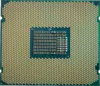 |
Skylake X | LGA-2066 | No | 2-chip | Lewisburg | DMI 3.0 | ✘ |
| Skylake SP | LGA-3647 | 2-chip + 2-8-way SMP | UPI |
Packages[edit]
| Core | Die Type | Package | Dimensions |
|---|---|---|---|
| Skylake SP | LCC | FCLGA-3647 | 76.16 mm x 56.6 mm |
| HCC | |||
| XCC | |||
| Skylake X | LCC | FCLGA-2066 | 58.5 mm x 51 mm |
| HCC |
Floorplan[edit]

All Skylake server dies consist of three major blocks:
- DDR PHYs
- North Cap
- Mesh Tiles
Those blocks are found on all die configuration and form the base for Intel's highly configurable floorplan. Depending on the market segment and model specification targets, Intel can add and remove rows of tiles.
_die_major_blocks_(xcc).png)
_die_major_blocks_(hcc).png)
Physical Layout[edit]
North Cap[edit]
The North Cap at the very top of the die contains all the I/O agents and PHYs as well as serial IP ports, and the fuse unit. For the most part this configuration largely the same for all the dies. For the smaller dies, the extras are removed (e.g., the in-package PCIe link is not needed).
At the very top of the North Cap are the various I/O connectivity. There are a total of 128 high-speed I/O lanes – 3×16 (48) PCIe lanes operating at 8 GT/s, x4 DMI lanes for hooking up the Lewisburg chipset, 16 on-package PCIe lanes (operating at 2.5/5/8 GT/s), and 3×20 (60) Ultra-Path Interconnect (UPI) lanes operating at 10.4 GT/s for the multiprocessing support.
At the south-west corner of the North Cap is the clock generator unit (CGU) and the Global Power Management Unit (Global PMU). The CGU contains an all-digital (AD) filter phase-locked loops (PLL) and an all-digital uncore PLL. The filter ADPLL is dedicated to the generation of all on-die reference clock used for all the core PLLs and one uncore PLL. The power management unit also has its own dedicated all-digital PLL.
At the bottom part of the North Cap are the Mesh stops for the various I/O to interface with the Mesh.
DDR PHYs[edit]
There are the two DDR4 PHYs which are identical for all the dies (albeit in the low-end models, the extra channel is simply disabled). There are two independent and identical physical sections of 3 DDR4 channels each which reside on the east and west edges of the die. Each channel is 72-bit (64 bit and an 8-bit ECC), supporting 2-DIMM per channel with a data rate of up to 2666 MT/s for a bandwidth of 21.33 GB/s and an aggregated bandwidth of 128 GB/s. RDIMM and LRDIMM are supported.
The location of the PHYs was carefully chosen in order to ease the package design, specifically, they were chosen in order to maintain escape routing and pin-out order matching between the CPU and the DIMM slots to shorten package and PCB routing length in order to improve signal integrity.
Layout[edit]
_die_area_layout.svg)
Evolution[edit]
The original Skylake large die started out as a 5 by 5 core tile (25 tiles, 25 cores) as shown by the image from Intel on the left side. The memory controllers were next to the PHYs on the east and west side. An additional row was inserted to get to a 5 by 6 grid. Two core tiles one from each of the sides was then replaced by the new memory controller module which can interface with the mesh just like any other core tile. The final die is shown in the image below as well on the right side.

Die[edit]
- See also: Client Skylake's Die

Skylake Server class models and high-end desktop (HEDT) consist of 3 different dies:
- 12 tiles (3x4), 10-core, Low Core Count (LCC)
- 20 tiles (5x4), 18-core, High Core Count (HCC)
- 30 tiles (5x6), 28-core, Extreme Core Count (XCC)
North Cap[edit]
HCC:
_northcap_(hcc).png)
_northcap_(hcc)_(annotated).png)
XCC:
_northcap_(xcc).png)
_northcap_(xcc)_(annotated).png)
Memory PHYs[edit]
Data bytes are located on the north and south sub-sections of the channel layout. Command, Control, Clock signals, and process, supply voltage, and temperature (PVT) compensation circuitry are located in the middle section of the channels.
.png)
Core Tile[edit]
- ~4.8375 x 3.7163
- ~ 17.978 mm² die area


Low Core Count (LCC)[edit]
- 14 nm process
- 12 metal layers
- ~22.26 mm x ~14.62 mm
- ~325.44 mm² die size
- 10 cores
- 12 tiles (3x4)
- (NOT official die shot, artist's rendering based on the larger die)
-
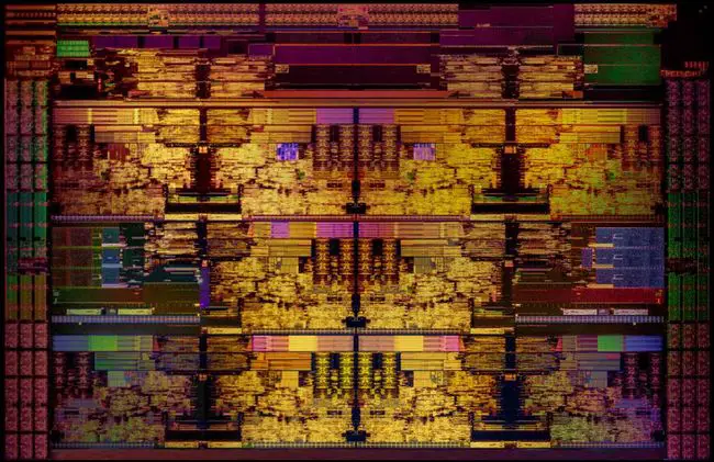

High Core Count (HCC)[edit]
Die shot of the octadeca core HEDT Skylake X processors.
- 14 nm process
- 13 metal layers
- ~485 mm² die size (estimated)
- 18 cores
- 20 tiles (5x4)
.png)
_(annotated).png)
Extreme Core Count (XCC)[edit]
- 14 nm process
- 13 metal layers
- ~694 mm² die size (estimated)
- 28 cores
- 30 tiles (5x6)

.png)
All Skylake Chips[edit]
| List of Skylake Processors | |||||||||||||||||||||||||
|---|---|---|---|---|---|---|---|---|---|---|---|---|---|---|---|---|---|---|---|---|---|---|---|---|---|
| Main processor | Frequency/Turbo | Mem | Major Feature Diff | ||||||||||||||||||||||
| Model | Launched | Price | Family | Core Name | Cores | Threads | L2$ | L3$ | TDP | Frequency | Max Turbo | Max Mem | Turbo | SMT | |||||||||||
| Uniprocessors | |||||||||||||||||||||||||
| i7-7800X | 26 June 2017 | $ 389.00 € 350.10 £ 315.09 ¥ 40,195.37 | Core i7 | Skylake X | 6 | 12 | 6 MiB 6,144 KiB 6,291,456 B 0.00586 GiB | 8.25 MiB 8,448 KiB 8,650,752 B 0.00806 GiB | 140 W 140,000 mW 0.188 hp 0.14 kW | 3.5 GHz 3,500 MHz 3,500,000 kHz | 4 GHz 4,000 MHz 4,000,000 kHz | 128 GiB 131,072 MiB 134,217,728 KiB 137,438,953,472 B 0.125 TiB | ✔ | ✔ | |||||||||||
| i7-7820X | 26 June 2017 | $ 599.00 € 539.10 £ 485.19 ¥ 61,894.67 | Core i7 | Skylake X | 8 | 16 | 8 MiB 8,192 KiB 8,388,608 B 0.00781 GiB | 11 MiB 11,264 KiB 11,534,336 B 0.0107 GiB | 140 W 140,000 mW 0.188 hp 0.14 kW | 3.6 GHz 3,600 MHz 3,600,000 kHz | 4.3 GHz 4,300 MHz 4,300,000 kHz | 128 GiB 131,072 MiB 134,217,728 KiB 137,438,953,472 B 0.125 TiB | ✔ | ✔ | |||||||||||
| i7-9800X | November 2018 | $ 589.00 € 530.10 £ 477.09 ¥ 60,861.37 | Core i7 | Skylake X Refresh | 8 | 16 | 8 MiB 8,192 KiB 8,388,608 B 0.00781 GiB | 16.5 MiB 16,896 KiB 17,301,504 B 0.0161 GiB | 165 W 165,000 mW 0.221 hp 0.165 kW | 3.8 GHz 3,800 MHz 3,800,000 kHz | 4.4 GHz 4,400 MHz 4,400,000 kHz | 128 GiB 131,072 MiB 134,217,728 KiB 137,438,953,472 B 0.125 TiB | ✔ | ✔ | |||||||||||
| i9-7900X | 26 June 2017 | $ 999.00 € 899.10 £ 809.19 ¥ 103,226.67 | Core i9 | Skylake X | 10 | 20 | 10 MiB 10,240 KiB 10,485,760 B 0.00977 GiB | 13.75 MiB 14,080 KiB 14,417,920 B 0.0134 GiB | 140 W 140,000 mW 0.188 hp 0.14 kW | 3.3 GHz 3,300 MHz 3,300,000 kHz | 4.3 GHz 4,300 MHz 4,300,000 kHz | 128 GiB 131,072 MiB 134,217,728 KiB 137,438,953,472 B 0.125 TiB | ✔ | ✔ | |||||||||||
| i9-7920X | 28 August 2017 | $ 1,199.00 € 1,079.10 £ 971.19 ¥ 123,892.67 | Core i9 | Skylake X | 12 | 24 | 12 MiB 12,288 KiB 12,582,912 B 0.0117 GiB | 16.5 MiB 16,896 KiB 17,301,504 B 0.0161 GiB | 140 W 140,000 mW 0.188 hp 0.14 kW | 2.9 GHz 2,900 MHz 2,900,000 kHz | 4.3 GHz 4,300 MHz 4,300,000 kHz | 128 GiB 131,072 MiB 134,217,728 KiB 137,438,953,472 B 0.125 TiB | ✔ | ✔ | |||||||||||
| i9-7940X | 25 September 2017 | $ 1,399.00 € 1,259.10 £ 1,133.19 ¥ 144,558.67 | Core i9 | Skylake X | 14 | 28 | 14 MiB 14,336 KiB 14,680,064 B 0.0137 GiB | 19.25 MiB 19,712 KiB 20,185,088 B 0.0188 GiB | 165 W 165,000 mW 0.221 hp 0.165 kW | 3.1 GHz 3,100 MHz 3,100,000 kHz | 4.3 GHz 4,300 MHz 4,300,000 kHz | 128 GiB 131,072 MiB 134,217,728 KiB 137,438,953,472 B 0.125 TiB | ✔ | ✔ | |||||||||||
| i9-7960X | 25 September 2017 | $ 1,699.00 € 1,529.10 £ 1,376.19 ¥ 175,557.67 | Core i9 | Skylake X | 16 | 32 | 16 MiB 16,384 KiB 16,777,216 B 0.0156 GiB | 22 MiB 22,528 KiB 23,068,672 B 0.0215 GiB | 165 W 165,000 mW 0.221 hp 0.165 kW | 2.8 GHz 2,800 MHz 2,800,000 kHz | 4.2 GHz 4,200 MHz 4,200,000 kHz | 128 GiB 131,072 MiB 134,217,728 KiB 137,438,953,472 B 0.125 TiB | ✔ | ✔ | |||||||||||
| i9-7980XE | 25 September 2017 | $ 1,999.00 € 1,799.10 £ 1,619.19 ¥ 206,556.67 | Core i9 | Skylake X | 18 | 36 | 18 MiB 18,432 KiB 18,874,368 B 0.0176 GiB | 24.75 MiB 25,344 KiB 25,952,256 B 0.0242 GiB | 165 W 165,000 mW 0.221 hp 0.165 kW | 2.6 GHz 2,600 MHz 2,600,000 kHz | 4.2 GHz 4,200 MHz 4,200,000 kHz | 128 GiB 131,072 MiB 134,217,728 KiB 137,438,953,472 B 0.125 TiB | ✔ | ✔ | |||||||||||
| i9-9820X | November 2018 | $ 898.00 € 808.20 £ 727.38 ¥ 92,790.34 | Core i9 | Skylake X Refresh | 10 | 20 | 10 MiB 10,240 KiB 10,485,760 B 0.00977 GiB | 16.5 MiB 16,896 KiB 17,301,504 B 0.0161 GiB | 165 W 165,000 mW 0.221 hp 0.165 kW | 3.3 GHz 3,300 MHz 3,300,000 kHz | 4.1 GHz 4,100 MHz 4,100,000 kHz | 128 GiB 131,072 MiB 134,217,728 KiB 137,438,953,472 B 0.125 TiB | ✔ | ✔ | |||||||||||
| i9-9900X | November 2018 | $ 989.00 € 890.10 £ 801.09 ¥ 102,193.37 | Core i9 | Skylake X Refresh | 10 | 20 | 10 MiB 10,240 KiB 10,485,760 B 0.00977 GiB | 19.25 MiB 19,712 KiB 20,185,088 B 0.0188 GiB | 165 W 165,000 mW 0.221 hp 0.165 kW | 3.5 GHz 3,500 MHz 3,500,000 kHz | 4.4 GHz 4,400 MHz 4,400,000 kHz | 128 GiB 131,072 MiB 134,217,728 KiB 137,438,953,472 B 0.125 TiB | ✔ | ✔ | |||||||||||
| i9-9920X | November 2018 | $ 1,189.00 € 1,070.10 £ 963.09 ¥ 122,859.37 | Core i9 | Skylake X Refresh | 12 | 24 | 12 MiB 12,288 KiB 12,582,912 B 0.0117 GiB | 19.25 MiB 19,712 KiB 20,185,088 B 0.0188 GiB | 165 W 165,000 mW 0.221 hp 0.165 kW | 3.5 GHz 3,500 MHz 3,500,000 kHz | 4.4 GHz 4,400 MHz 4,400,000 kHz | 128 GiB 131,072 MiB 134,217,728 KiB 137,438,953,472 B 0.125 TiB | ✔ | ✔ | |||||||||||
| i9-9940X | November 2018 | $ 1,387.00 € 1,248.30 £ 1,123.47 ¥ 143,318.71 | Core i9 | Skylake X Refresh | 14 | 28 | 14 MiB 14,336 KiB 14,680,064 B 0.0137 GiB | 19.25 MiB 19,712 KiB 20,185,088 B 0.0188 GiB | 165 W 165,000 mW 0.221 hp 0.165 kW | 3.3 GHz 3,300 MHz 3,300,000 kHz | 4.4 GHz 4,400 MHz 4,400,000 kHz | 128 GiB 131,072 MiB 134,217,728 KiB 137,438,953,472 B 0.125 TiB | ✔ | ✔ | |||||||||||
| i9-9960X | November 2018 | $ 1,684.00 € 1,515.60 £ 1,364.04 ¥ 174,007.72 | Core i9 | Skylake X Refresh | 16 | 32 | 16 MiB 16,384 KiB 16,777,216 B 0.0156 GiB | 22 MiB 22,528 KiB 23,068,672 B 0.0215 GiB | 165 W 165,000 mW 0.221 hp 0.165 kW | 3.1 GHz 3,100 MHz 3,100,000 kHz | 4.4 GHz 4,400 MHz 4,400,000 kHz | 128 GiB 131,072 MiB 134,217,728 KiB 137,438,953,472 B 0.125 TiB | ✔ | ✔ | |||||||||||
| i9-9980XE | November 2018 | $ 1,979.00 € 1,781.10 £ 1,602.99 ¥ 204,490.07 | Core i9 | Skylake X Refresh | 18 | 36 | 18 MiB 18,432 KiB 18,874,368 B 0.0176 GiB | 24.75 MiB 25,344 KiB 25,952,256 B 0.0242 GiB | 165 W 165,000 mW 0.221 hp 0.165 kW | 3 GHz 3,000 MHz 3,000,000 kHz | 4.4 GHz 4,400 MHz 4,400,000 kHz | 128 GiB 131,072 MiB 134,217,728 KiB 137,438,953,472 B 0.125 TiB | ✔ | ✔ | |||||||||||
| i9-9990XE | 3 January 2019 | Core i9 | Skylake X Refresh | 14 | 28 | 14 MiB 14,336 KiB 14,680,064 B 0.0137 GiB | 19.25 MiB 19,712 KiB 20,185,088 B 0.0188 GiB | 255 W 255,000 mW 0.342 hp 0.255 kW | 4 GHz 4,000 MHz 4,000,000 kHz | 5 GHz 5,000 MHz 5,000,000 kHz | 128 GiB 131,072 MiB 134,217,728 KiB 137,438,953,472 B 0.125 TiB | ✔ | ✔ | ||||||||||||
| D-2123IT | 7 February 2018 | $ 213.00 € 191.70 £ 172.53 ¥ 22,009.29 | Xeon D | Skylake DE | 4 | 8 | 4 MiB 4,096 KiB 4,194,304 B 0.00391 GiB | 8.25 MiB 8,448 KiB 8,650,752 B 0.00806 GiB | 60 W 60,000 mW 0.0805 hp 0.06 kW | 2.2 GHz 2,200 MHz 2,200,000 kHz | 3 GHz 3,000 MHz 3,000,000 kHz | 512 GiB 524,288 MiB 536,870,912 KiB 549,755,813,888 B 0.5 TiB | ✔ | ✔ | |||||||||||
| D-2141I | 7 February 2018 | $ 555.00 € 499.50 £ 449.55 ¥ 57,348.15 | Xeon D | Skylake DE | 8 | 16 | 8 MiB 8,192 KiB 8,388,608 B 0.00781 GiB | 11 MiB 11,264 KiB 11,534,336 B 0.0107 GiB | 65 W 65,000 mW 0.0872 hp 0.065 kW | 2.2 GHz 2,200 MHz 2,200,000 kHz | 3 GHz 3,000 MHz 3,000,000 kHz | 512 GiB 524,288 MiB 536,870,912 KiB 549,755,813,888 B 0.5 TiB | ✔ | ✔ | |||||||||||
| D-2142IT | 7 February 2018 | $ 438.00 € 394.20 £ 354.78 ¥ 45,258.54 | Xeon D | Skylake DE | 8 | 16 | 8 MiB 8,192 KiB 8,388,608 B 0.00781 GiB | 11 MiB 11,264 KiB 11,534,336 B 0.0107 GiB | 65 W 65,000 mW 0.0872 hp 0.065 kW | 1.9 GHz 1,900 MHz 1,900,000 kHz | 3 GHz 3,000 MHz 3,000,000 kHz | 512 GiB 524,288 MiB 536,870,912 KiB 549,755,813,888 B 0.5 TiB | ✔ | ✔ | |||||||||||
| D-2143IT | 7 February 2018 | $ 566.00 € 509.40 £ 458.46 ¥ 58,484.78 | Xeon D | Skylake DE | 8 | 16 | 8 MiB 8,192 KiB 8,388,608 B 0.00781 GiB | 11 MiB 11,264 KiB 11,534,336 B 0.0107 GiB | 65 W 65,000 mW 0.0872 hp 0.065 kW | 2.2 GHz 2,200 MHz 2,200,000 kHz | 3 GHz 3,000 MHz 3,000,000 kHz | 512 GiB 524,288 MiB 536,870,912 KiB 549,755,813,888 B 0.5 TiB | ✔ | ✔ | |||||||||||
| D-2145NT | 7 February 2018 | $ 502.00 € 451.80 £ 406.62 ¥ 51,871.66 | Xeon D | Skylake DE | 8 | 16 | 8 MiB 8,192 KiB 8,388,608 B 0.00781 GiB | 11 MiB 11,264 KiB 11,534,336 B 0.0107 GiB | 65 W 65,000 mW 0.0872 hp 0.065 kW | 1.9 GHz 1,900 MHz 1,900,000 kHz | 3 GHz 3,000 MHz 3,000,000 kHz | 512 GiB 524,288 MiB 536,870,912 KiB 549,755,813,888 B 0.5 TiB | ✔ | ✔ | |||||||||||
| D-2146NT | 7 February 2018 | $ 641.00 € 576.90 £ 519.21 ¥ 66,234.53 | Xeon D | Skylake DE | 8 | 16 | 8 MiB 8,192 KiB 8,388,608 B 0.00781 GiB | 11 MiB 11,264 KiB 11,534,336 B 0.0107 GiB | 80 W 80,000 mW 0.107 hp 0.08 kW | 2.3 GHz 2,300 MHz 2,300,000 kHz | 3 GHz 3,000 MHz 3,000,000 kHz | 512 GiB 524,288 MiB 536,870,912 KiB 549,755,813,888 B 0.5 TiB | ✔ | ✔ | |||||||||||
| D-2161I | 7 February 2018 | $ 962.00 € 865.80 £ 779.22 ¥ 99,403.46 | Xeon D | Skylake DE | 12 | 24 | 12 MiB 12,288 KiB 12,582,912 B 0.0117 GiB | 16.5 MiB 16,896 KiB 17,301,504 B 0.0161 GiB | 90 W 90,000 mW 0.121 hp 0.09 kW | 2.2 GHz 2,200 MHz 2,200,000 kHz | 3 GHz 3,000 MHz 3,000,000 kHz | 512 GiB 524,288 MiB 536,870,912 KiB 549,755,813,888 B 0.5 TiB | ✔ | ✔ | |||||||||||
| D-2163IT | 7 February 2018 | $ 930.00 € 837.00 £ 753.30 ¥ 96,096.90 | Xeon D | Skylake DE | 12 | 24 | 12 MiB 12,288 KiB 12,582,912 B 0.0117 GiB | 16.5 MiB 16,896 KiB 17,301,504 B 0.0161 GiB | 75 W 75,000 mW 0.101 hp 0.075 kW | 2.1 GHz 2,100 MHz 2,100,000 kHz | 3 GHz 3,000 MHz 3,000,000 kHz | 512 GiB 524,288 MiB 536,870,912 KiB 549,755,813,888 B 0.5 TiB | ✔ | ✔ | |||||||||||
| D-2166NT | 7 February 2018 | $ 1,005.00 € 904.50 £ 814.05 ¥ 103,846.65 | Xeon D | Skylake DE | 12 | 24 | 12 MiB 12,288 KiB 12,582,912 B 0.0117 GiB | 16.5 MiB 16,896 KiB 17,301,504 B 0.0161 GiB | 85 W 85,000 mW 0.114 hp 0.085 kW | 2 GHz 2,000 MHz 2,000,000 kHz | 3 GHz 3,000 MHz 3,000,000 kHz | 512 GiB 524,288 MiB 536,870,912 KiB 549,755,813,888 B 0.5 TiB | ✔ | ✔ | |||||||||||
| D-2173IT | 7 February 2018 | $ 1,229.00 € 1,106.10 £ 995.49 ¥ 126,992.57 | Xeon D | Skylake DE | 14 | 28 | 14 MiB 14,336 KiB 14,680,064 B 0.0137 GiB | 19.25 MiB 19,712 KiB 20,185,088 B 0.0188 GiB | 70 W 70,000 mW 0.0939 hp 0.07 kW | 1.7 GHz 1,700 MHz 1,700,000 kHz | 3 GHz 3,000 MHz 3,000,000 kHz | 512 GiB 524,288 MiB 536,870,912 KiB 549,755,813,888 B 0.5 TiB | ✔ | ✔ | |||||||||||
| D-2177NT | 7 February 2018 | $ 1,443.00 € 1,298.70 £ 1,168.83 ¥ 149,105.19 | Xeon D | Skylake DE | 14 | 28 | 14 MiB 14,336 KiB 14,680,064 B 0.0137 GiB | 19.25 MiB 19,712 KiB 20,185,088 B 0.0188 GiB | 105 W 105,000 mW 0.141 hp 0.105 kW | 1.9 GHz 1,900 MHz 1,900,000 kHz | 3 GHz 3,000 MHz 3,000,000 kHz | 512 GiB 524,288 MiB 536,870,912 KiB 549,755,813,888 B 0.5 TiB | ✔ | ✔ | |||||||||||
| D-2183IT | 7 February 2018 | $ 1,764.00 € 1,587.60 £ 1,428.84 ¥ 182,274.12 | Xeon D | Skylake DE | 16 | 32 | 16 MiB 16,384 KiB 16,777,216 B 0.0156 GiB | 22 MiB 22,528 KiB 23,068,672 B 0.0215 GiB | 100 W 100,000 mW 0.134 hp 0.1 kW | 2.2 GHz 2,200 MHz 2,200,000 kHz | 3 GHz 3,000 MHz 3,000,000 kHz | 512 GiB 524,288 MiB 536,870,912 KiB 549,755,813,888 B 0.5 TiB | ✔ | ✔ | |||||||||||
| D-2187NT | 7 February 2018 | $ 1,989.00 € 1,790.10 £ 1,611.09 ¥ 205,523.37 | Xeon D | Skylake DE | 16 | 32 | 16 MiB 16,384 KiB 16,777,216 B 0.0156 GiB | 22 MiB 22,528 KiB 23,068,672 B 0.0215 GiB | 110 W 110,000 mW 0.148 hp 0.11 kW | 2 GHz 2,000 MHz 2,000,000 kHz | 3 GHz 3,000 MHz 3,000,000 kHz | 512 GiB 524,288 MiB 536,870,912 KiB 549,755,813,888 B 0.5 TiB | ✔ | ✔ | |||||||||||
| D-2191 | 7 February 2018 | $ 2,406.00 € 2,165.40 £ 1,948.86 ¥ 248,611.98 | Xeon D | Skylake DE | 18 | 36 | 18 MiB 18,432 KiB 18,874,368 B 0.0176 GiB | 24.75 MiB 25,344 KiB 25,952,256 B 0.0242 GiB | 86 W 86,000 mW 0.115 hp 0.086 kW | 1.6 GHz 1,600 MHz 1,600,000 kHz | 3 GHz 3,000 MHz 3,000,000 kHz | 512 GiB 524,288 MiB 536,870,912 KiB 549,755,813,888 B 0.5 TiB | ✔ | ✔ | |||||||||||
| W-2102 | 29 August 2017 | $ 202.00 € 181.80 £ 163.62 ¥ 20,872.66 | Xeon W | Skylake W | 4 | 4 | 4 MiB 4,096 KiB 4,194,304 B 0.00391 GiB | 8.25 MiB 8,448 KiB 8,650,752 B 0.00806 GiB | 120 W 120,000 mW 0.161 hp 0.12 kW | 2.9 GHz 2,900 MHz 2,900,000 kHz | 512 GiB 524,288 MiB 536,870,912 KiB 549,755,813,888 B 0.5 TiB | ✘ | ✘ | ||||||||||||
| W-2104 | 29 August 2017 | $ 255.00 € 229.50 £ 206.55 ¥ 26,349.15 | Xeon W | Skylake W | 4 | 4 | 4 MiB 4,096 KiB 4,194,304 B 0.00391 GiB | 8.25 MiB 8,448 KiB 8,650,752 B 0.00806 GiB | 120 W 120,000 mW 0.161 hp 0.12 kW | 3.2 GHz 3,200 MHz 3,200,000 kHz | 512 GiB 524,288 MiB 536,870,912 KiB 549,755,813,888 B 0.5 TiB | ✘ | ✘ | ||||||||||||
| W-2123 | 29 August 2017 | $ 294.00 € 264.60 £ 238.14 ¥ 30,379.02 | Xeon W | Skylake W | 4 | 8 | 4 MiB 4,096 KiB 4,194,304 B 0.00391 GiB | 8.25 MiB 8,448 KiB 8,650,752 B 0.00806 GiB | 120 W 120,000 mW 0.161 hp 0.12 kW | 3.6 GHz 3,600 MHz 3,600,000 kHz | 3.9 GHz 3,900 MHz 3,900,000 kHz | 512 GiB 524,288 MiB 536,870,912 KiB 549,755,813,888 B 0.5 TiB | ✔ | ✔ | |||||||||||
| W-2125 | 29 August 2017 | $ 444.00 € 399.60 £ 359.64 ¥ 45,878.52 | Xeon W | Skylake W | 4 | 8 | 4 MiB 4,096 KiB 4,194,304 B 0.00391 GiB | 8.25 MiB 8,448 KiB 8,650,752 B 0.00806 GiB | 120 W 120,000 mW 0.161 hp 0.12 kW | 4 GHz 4,000 MHz 4,000,000 kHz | 4.5 GHz 4,500 MHz 4,500,000 kHz | 512 GiB 524,288 MiB 536,870,912 KiB 549,755,813,888 B 0.5 TiB | ✔ | ✔ | |||||||||||
| W-2133 | 29 August 2017 | $ 617.00 € 555.30 £ 499.77 ¥ 63,754.61 | Xeon W | Skylake W | 6 | 12 | 6 MiB 6,144 KiB 6,291,456 B 0.00586 GiB | 8.25 MiB 8,448 KiB 8,650,752 B 0.00806 GiB | 140 W 140,000 mW 0.188 hp 0.14 kW | 3.6 GHz 3,600 MHz 3,600,000 kHz | 3.9 GHz 3,900 MHz 3,900,000 kHz | 512 GiB 524,288 MiB 536,870,912 KiB 549,755,813,888 B 0.5 TiB | ✔ | ✔ | |||||||||||
| W-2135 | 29 August 2017 | $ 835.00 € 751.50 £ 676.35 ¥ 86,280.55 | Xeon W | Skylake W | 6 | 12 | 6 MiB 6,144 KiB 6,291,456 B 0.00586 GiB | 8.25 MiB 8,448 KiB 8,650,752 B 0.00806 GiB | 140 W 140,000 mW 0.188 hp 0.14 kW | 3.7 GHz 3,700 MHz 3,700,000 kHz | 4.5 GHz 4,500 MHz 4,500,000 kHz | 512 GiB 524,288 MiB 536,870,912 KiB 549,755,813,888 B 0.5 TiB | ✔ | ✔ | |||||||||||
| W-2140B | 21 December 2017 | Xeon W | Skylake W | 8 | 16 | 8 MiB 8,192 KiB 8,388,608 B 0.00781 GiB | 11 MiB 11,264 KiB 11,534,336 B 0.0107 GiB | 3.2 GHz 3,200 MHz 3,200,000 kHz | 4.2 GHz 4,200 MHz 4,200,000 kHz | 512 GiB 524,288 MiB 536,870,912 KiB 549,755,813,888 B 0.5 TiB | ✔ | ✔ | |||||||||||||
| W-2145 | 29 August 2017 | $ 1,113.00 € 1,001.70 £ 901.53 ¥ 115,006.29 | Xeon W | Skylake W | 8 | 16 | 8 MiB 8,192 KiB 8,388,608 B 0.00781 GiB | 11 MiB 11,264 KiB 11,534,336 B 0.0107 GiB | 140 W 140,000 mW 0.188 hp 0.14 kW | 3.7 GHz 3,700 MHz 3,700,000 kHz | 4.5 GHz 4,500 MHz 4,500,000 kHz | 512 GiB 524,288 MiB 536,870,912 KiB 549,755,813,888 B 0.5 TiB | ✔ | ✔ | |||||||||||
| W-2150B | 21 December 2017 | Xeon W | Skylake W | 10 | 20 | 10 MiB 10,240 KiB 10,485,760 B 0.00977 GiB | 13.75 MiB 14,080 KiB 14,417,920 B 0.0134 GiB | 3 GHz 3,000 MHz 3,000,000 kHz | 4.5 GHz 4,500 MHz 4,500,000 kHz | 512 GiB 524,288 MiB 536,870,912 KiB 549,755,813,888 B 0.5 TiB | ✔ | ✔ | |||||||||||||
| W-2155 | 29 August 2017 | $ 1,440.00 € 1,296.00 £ 1,166.40 ¥ 148,795.20 | Xeon W | Skylake W | 10 | 20 | 10 MiB 10,240 KiB 10,485,760 B 0.00977 GiB | 13.75 MiB 14,080 KiB 14,417,920 B 0.0134 GiB | 140 W 140,000 mW 0.188 hp 0.14 kW | 3.3 GHz 3,300 MHz 3,300,000 kHz | 4.5 GHz 4,500 MHz 4,500,000 kHz | 512 GiB 524,288 MiB 536,870,912 KiB 549,755,813,888 B 0.5 TiB | ✔ | ✔ | |||||||||||
| W-2170B | 21 December 2017 | Xeon W | Skylake W | 14 | 28 | 14 MiB 14,336 KiB 14,680,064 B 0.0137 GiB | 19.25 MiB 19,712 KiB 20,185,088 B 0.0188 GiB | 2.5 GHz 2,500 MHz 2,500,000 kHz | 4.3 GHz 4,300 MHz 4,300,000 kHz | 512 GiB 524,288 MiB 536,870,912 KiB 549,755,813,888 B 0.5 TiB | ✔ | ✔ | |||||||||||||
| W-2175 | 29 August 2017 | $ 1,947.00 € 1,752.30 £ 1,577.07 ¥ 201,183.51 | Xeon W | Skylake W | 14 | 28 | 14 MiB 14,336 KiB 14,680,064 B 0.0137 GiB | 19.25 MiB 19,712 KiB 20,185,088 B 0.0188 GiB | 140 W 140,000 mW 0.188 hp 0.14 kW | 2.5 GHz 2,500 MHz 2,500,000 kHz | 4.3 GHz 4,300 MHz 4,300,000 kHz | 512 GiB 524,288 MiB 536,870,912 KiB 549,755,813,888 B 0.5 TiB | ✔ | ✔ | |||||||||||
| W-2191B | 21 December 2017 | Xeon W | Skylake W | 18 | 36 | 18 MiB 18,432 KiB 18,874,368 B 0.0176 GiB | 24.75 MiB 25,344 KiB 25,952,256 B 0.0242 GiB | 2.3 GHz 2,300 MHz 2,300,000 kHz | 4.3 GHz 4,300 MHz 4,300,000 kHz | 512 GiB 524,288 MiB 536,870,912 KiB 549,755,813,888 B 0.5 TiB | ✔ | ✔ | |||||||||||||
| W-2195 | 29 August 2017 | $ 2,553.00 € 2,297.70 £ 2,067.93 ¥ 263,801.49 | Xeon W | Skylake W | 18 | 36 | 18 MiB 18,432 KiB 18,874,368 B 0.0176 GiB | 24.75 MiB 25,344 KiB 25,952,256 B 0.0242 GiB | 140 W 140,000 mW 0.188 hp 0.14 kW | 2.3 GHz 2,300 MHz 2,300,000 kHz | 4.3 GHz 4,300 MHz 4,300,000 kHz | 512 GiB 524,288 MiB 536,870,912 KiB 549,755,813,888 B 0.5 TiB | ✔ | ✔ | |||||||||||
| W-3175X | 30 January 2019 | $ 2,999.00 € 2,699.10 £ 2,429.19 ¥ 309,886.67 | Xeon W | Skylake SP | 28 | 56 | 28 MiB 28,672 KiB 29,360,128 B 0.0273 GiB | 38.5 MiB 39,424 KiB 40,370,176 B 0.0376 GiB | 255 W 255,000 mW 0.342 hp 0.255 kW | 3.1 GHz 3,100 MHz 3,100,000 kHz | 4.3 GHz 4,300 MHz 4,300,000 kHz | 512 GiB 524,288 MiB 536,870,912 KiB 549,755,813,888 B 0.5 TiB | ✔ | ✔ | |||||||||||
| Multiprocessors (2-way) | |||||||||||||||||||||||||
| 3104 | 11 July 2017 | $ 213.00 € 191.70 £ 172.53 ¥ 22,009.29 | Xeon Bronze | Skylake SP | 6 | 6 | 6 MiB 6,144 KiB 6,291,456 B 0.00586 GiB | 8.25 MiB 8,448 KiB 8,650,752 B 0.00806 GiB | 85 W 85,000 mW 0.114 hp 0.085 kW | 1.7 GHz 1,700 MHz 1,700,000 kHz | 768 GiB 786,432 MiB 805,306,368 KiB 824,633,720,832 B 0.75 TiB | ✘ | ✘ | ||||||||||||
| 3106 | 11 July 2017 | $ 306.00 € 275.40 £ 247.86 ¥ 31,618.98 | Xeon Bronze | Skylake SP | 8 | 8 | 8 MiB 8,192 KiB 8,388,608 B 0.00781 GiB | 11 MiB 11,264 KiB 11,534,336 B 0.0107 GiB | 85 W 85,000 mW 0.114 hp 0.085 kW | 1.7 GHz 1,700 MHz 1,700,000 kHz | 768 GiB 786,432 MiB 805,306,368 KiB 824,633,720,832 B 0.75 TiB | ✘ | ✘ | ||||||||||||
| 6138P | 16 May 2018 | $ 4,937.00 € 4,443.30 £ 3,998.97 ¥ 510,140.21 | Xeon Gold | Skylake SP | 20 | 40 | 20 MiB 20,480 KiB 20,971,520 B 0.0195 GiB | 27.5 MiB 28,160 KiB 28,835,840 B 0.0269 GiB | 195 W 195,000 mW 0.261 hp 0.195 kW | 2 GHz 2,000 MHz 2,000,000 kHz | 3.7 GHz 3,700 MHz 3,700,000 kHz | 768 GiB 786,432 MiB 805,306,368 KiB 824,633,720,832 B 0.75 TiB | ✔ | ✔ | |||||||||||
| 4108 | 11 July 2017 | $ 417.00 € 375.30 £ 337.77 ¥ 43,088.61 | Xeon Silver | Skylake SP | 8 | 16 | 8 MiB 8,192 KiB 8,388,608 B 0.00781 GiB | 11 MiB 11,264 KiB 11,534,336 B 0.0107 GiB | 85 W 85,000 mW 0.114 hp 0.085 kW | 1.8 GHz 1,800 MHz 1,800,000 kHz | 3 GHz 3,000 MHz 3,000,000 kHz | 768 GiB 786,432 MiB 805,306,368 KiB 824,633,720,832 B 0.75 TiB | ✔ | ✔ | |||||||||||
| 4109T | 11 July 2017 | $ 501.00 € 450.90 £ 405.81 ¥ 51,768.33 | Xeon Silver | Skylake SP | 8 | 16 | 8 MiB 8,192 KiB 8,388,608 B 0.00781 GiB | 11 MiB 11,264 KiB 11,534,336 B 0.0107 GiB | 70 W 70,000 mW 0.0939 hp 0.07 kW | 2 GHz 2,000 MHz 2,000,000 kHz | 3 GHz 3,000 MHz 3,000,000 kHz | 768 GiB 786,432 MiB 805,306,368 KiB 824,633,720,832 B 0.75 TiB | ✔ | ✔ | |||||||||||
| 4110 | 11 July 2017 | $ 501.00 € 450.90 £ 405.81 ¥ 51,768.33 | Xeon Silver | Skylake SP | 8 | 16 | 8 MiB 8,192 KiB 8,388,608 B 0.00781 GiB | 11 MiB 11,264 KiB 11,534,336 B 0.0107 GiB | 85 W 85,000 mW 0.114 hp 0.085 kW | 2.1 GHz 2,100 MHz 2,100,000 kHz | 3 GHz 3,000 MHz 3,000,000 kHz | 768 GiB 786,432 MiB 805,306,368 KiB 824,633,720,832 B 0.75 TiB | ✔ | ✔ | |||||||||||
| 4112 | 11 July 2017 | $ 473.00 € 425.70 £ 383.13 ¥ 48,875.09 | Xeon Silver | Skylake SP | 4 | 8 | 4 MiB 4,096 KiB 4,194,304 B 0.00391 GiB | 8.25 MiB 8,448 KiB 8,650,752 B 0.00806 GiB | 85 W 85,000 mW 0.114 hp 0.085 kW | 2.6 GHz 2,600 MHz 2,600,000 kHz | 3 GHz 3,000 MHz 3,000,000 kHz | 768 GiB 786,432 MiB 805,306,368 KiB 824,633,720,832 B 0.75 TiB | ✔ | ✔ | |||||||||||
| 4114 | 11 July 2017 | $ 694.00 € 624.60 £ 562.14 ¥ 71,711.02 | Xeon Silver | Skylake SP | 10 | 20 | 10 MiB 10,240 KiB 10,485,760 B 0.00977 GiB | 13.75 MiB 14,080 KiB 14,417,920 B 0.0134 GiB | 85 W 85,000 mW 0.114 hp 0.085 kW | 2.2 GHz 2,200 MHz 2,200,000 kHz | 3 GHz 3,000 MHz 3,000,000 kHz | 768 GiB 786,432 MiB 805,306,368 KiB 824,633,720,832 B 0.75 TiB | ✔ | ✔ | |||||||||||
| 4114T | 11 July 2017 | Xeon Silver | Skylake SP | 10 | 20 | 10 MiB 10,240 KiB 10,485,760 B 0.00977 GiB | 13.75 MiB 14,080 KiB 14,417,920 B 0.0134 GiB | 85 W 85,000 mW 0.114 hp 0.085 kW | 2.2 GHz 2,200 MHz 2,200,000 kHz | 3 GHz 3,000 MHz 3,000,000 kHz | 768 GiB 786,432 MiB 805,306,368 KiB 824,633,720,832 B 0.75 TiB | ✔ | ✔ | ||||||||||||
| 4116 | 11 July 2017 | $ 1,002.00 € 901.80 £ 811.62 ¥ 103,536.66 | Xeon Silver | Skylake SP | 12 | 24 | 12 MiB 12,288 KiB 12,582,912 B 0.0117 GiB | 16.5 MiB 16,896 KiB 17,301,504 B 0.0161 GiB | 85 W 85,000 mW 0.114 hp 0.085 kW | 2.1 GHz 2,100 MHz 2,100,000 kHz | 3 GHz 3,000 MHz 3,000,000 kHz | 768 GiB 786,432 MiB 805,306,368 KiB 824,633,720,832 B 0.75 TiB | ✔ | ✔ | |||||||||||
| 4116T | 11 July 2017 | Xeon Silver | Skylake SP | 12 | 24 | 12 MiB 12,288 KiB 12,582,912 B 0.0117 GiB | 16.5 MiB 16,896 KiB 17,301,504 B 0.0161 GiB | 85 W 85,000 mW 0.114 hp 0.085 kW | 2.1 GHz 2,100 MHz 2,100,000 kHz | 3 GHz 3,000 MHz 3,000,000 kHz | 768 GiB 786,432 MiB 805,306,368 KiB 824,633,720,832 B 0.75 TiB | ✔ | ✔ | ||||||||||||
| Multiprocessors (4-way) | |||||||||||||||||||||||||
| 5115 | 11 July 2017 | $ 1,221.00 € 1,098.90 £ 989.01 ¥ 126,165.93 | Xeon Gold | Skylake SP | 10 | 20 | 10 MiB 10,240 KiB 10,485,760 B 0.00977 GiB | 13.75 MiB 14,080 KiB 14,417,920 B 0.0134 GiB | 85 W 85,000 mW 0.114 hp 0.085 kW | 2.4 GHz 2,400 MHz 2,400,000 kHz | 3.2 GHz 3,200 MHz 3,200,000 kHz | 768 GiB 786,432 MiB 805,306,368 KiB 824,633,720,832 B 0.75 TiB | ✔ | ✔ | |||||||||||
| 5117 | 11 July 2017 | Xeon Gold | Skylake SP | 14 | 28 | 14 MiB 14,336 KiB 14,680,064 B 0.0137 GiB | 19.25 MiB 19,712 KiB 20,185,088 B 0.0188 GiB | 105 W 105,000 mW 0.141 hp 0.105 kW | 2 GHz 2,000 MHz 2,000,000 kHz | 2.8 GHz 2,800 MHz 2,800,000 kHz | 768 GiB 786,432 MiB 805,306,368 KiB 824,633,720,832 B 0.75 TiB | ✔ | ✔ | ||||||||||||
| 5117F | 11 July 2017 | Xeon Gold | Skylake SP | 14 | 28 | 14 MiB 14,336 KiB 14,680,064 B 0.0137 GiB | 19.25 MiB 19,712 KiB 20,185,088 B 0.0188 GiB | 113 W 113,000 mW 0.152 hp 0.113 kW | 2 GHz 2,000 MHz 2,000,000 kHz | 2.8 GHz 2,800 MHz 2,800,000 kHz | 768 GiB 786,432 MiB 805,306,368 KiB 824,633,720,832 B 0.75 TiB | ✔ | ✔ | ||||||||||||
| 5118 | 11 July 2017 | $ 1,273.00 € 1,145.70 £ 1,031.13 ¥ 131,539.09 | Xeon Gold | Skylake SP | 12 | 24 | 12 MiB 12,288 KiB 12,582,912 B 0.0117 GiB | 16.5 MiB 16,896 KiB 17,301,504 B 0.0161 GiB | 105 W 105,000 mW 0.141 hp 0.105 kW | 2.3 GHz 2,300 MHz 2,300,000 kHz | 3.2 GHz 3,200 MHz 3,200,000 kHz | 768 GiB 786,432 MiB 805,306,368 KiB 824,633,720,832 B 0.75 TiB | ✔ | ✔ | |||||||||||
| 5119T | 11 July 2017 | Xeon Gold | Skylake SP | 14 | 28 | 14 MiB 14,336 KiB 14,680,064 B 0.0137 GiB | 19.25 MiB 19,712 KiB 20,185,088 B 0.0188 GiB | 85 W 85,000 mW 0.114 hp 0.085 kW | 1.9 GHz 1,900 MHz 1,900,000 kHz | 3.2 GHz 3,200 MHz 3,200,000 kHz | 768 GiB 786,432 MiB 805,306,368 KiB 824,633,720,832 B 0.75 TiB | ✔ | ✔ | ||||||||||||
| 5120 | 11 July 2017 | $ 1,555.00 € 1,399.50 £ 1,259.55 ¥ 160,678.15 | Xeon Gold | Skylake SP | 14 | 28 | 14 MiB 14,336 KiB 14,680,064 B 0.0137 GiB | 19.25 MiB 19,712 KiB 20,185,088 B 0.0188 GiB | 105 W 105,000 mW 0.141 hp 0.105 kW | 2.2 GHz 2,200 MHz 2,200,000 kHz | 3.2 GHz 3,200 MHz 3,200,000 kHz | 768 GiB 786,432 MiB 805,306,368 KiB 824,633,720,832 B 0.75 TiB | ✔ | ✔ | |||||||||||
| 5120T | 11 July 2017 | $ 1,727.00 € 1,554.30 £ 1,398.87 ¥ 178,450.91 | Xeon Gold | Skylake SP | 14 | 28 | 14 MiB 14,336 KiB 14,680,064 B 0.0137 GiB | 19.25 MiB 19,712 KiB 20,185,088 B 0.0188 GiB | 105 W 105,000 mW 0.141 hp 0.105 kW | 2.2 GHz 2,200 MHz 2,200,000 kHz | 3.2 GHz 3,200 MHz 3,200,000 kHz | 768 GiB 786,432 MiB 805,306,368 KiB 824,633,720,832 B 0.75 TiB | ✔ | ✔ | |||||||||||
| 5122 | 11 July 2017 | $ 1,221.00 € 1,098.90 £ 989.01 ¥ 126,165.93 | Xeon Gold | Skylake SP | 4 | 8 | 4 MiB 4,096 KiB 4,194,304 B 0.00391 GiB | 16.5 MiB 16,896 KiB 17,301,504 B 0.0161 GiB | 105 W 105,000 mW 0.141 hp 0.105 kW | 3.6 GHz 3,600 MHz 3,600,000 kHz | 3.7 GHz 3,700 MHz 3,700,000 kHz | 768 GiB 786,432 MiB 805,306,368 KiB 824,633,720,832 B 0.75 TiB | ✔ | ✔ | |||||||||||
| 6126 | 11 July 2017 | $ 1,776.00 € 1,598.40 £ 1,438.56 ¥ 183,514.08 | Xeon Gold | Skylake SP | 12 | 24 | 12 MiB 12,288 KiB 12,582,912 B 0.0117 GiB | 19.25 MiB 19,712 KiB 20,185,088 B 0.0188 GiB | 125 W 125,000 mW 0.168 hp 0.125 kW | 2.6 GHz 2,600 MHz 2,600,000 kHz | 3.7 GHz 3,700 MHz 3,700,000 kHz | 768 GiB 786,432 MiB 805,306,368 KiB 824,633,720,832 B 0.75 TiB | ✔ | ✔ | |||||||||||
| 6126F | 11 July 2017 | $ 1,931.00 € 1,737.90 £ 1,564.11 ¥ 199,530.23 | Xeon Gold | Skylake SP | 12 | 24 | 12 MiB 12,288 KiB 12,582,912 B 0.0117 GiB | 19.25 MiB 19,712 KiB 20,185,088 B 0.0188 GiB | 135 W 135,000 mW 0.181 hp 0.135 kW | 2.6 GHz 2,600 MHz 2,600,000 kHz | 3.7 GHz 3,700 MHz 3,700,000 kHz | 768 GiB 786,432 MiB 805,306,368 KiB 824,633,720,832 B 0.75 TiB | ✔ | ✔ | |||||||||||
| 6126T | 11 July 2017 | $ 1,865.00 € 1,678.50 £ 1,510.65 ¥ 192,710.45 | Xeon Gold | Skylake SP | 12 | 24 | 12 MiB 12,288 KiB 12,582,912 B 0.0117 GiB | 19.25 MiB 19,712 KiB 20,185,088 B 0.0188 GiB | 125 W 125,000 mW 0.168 hp 0.125 kW | 2.6 GHz 2,600 MHz 2,600,000 kHz | 3.7 GHz 3,700 MHz 3,700,000 kHz | 768 GiB 786,432 MiB 805,306,368 KiB 824,633,720,832 B 0.75 TiB | ✔ | ✔ | |||||||||||
| 6128 | 11 July 2017 | $ 1,697.00 € 1,527.30 £ 1,374.57 ¥ 175,351.01 | Xeon Gold | Skylake SP | 6 | 12 | 6 MiB 6,144 KiB 6,291,456 B 0.00586 GiB | 19.25 MiB 19,712 KiB 20,185,088 B 0.0188 GiB | 115 W 115,000 mW 0.154 hp 0.115 kW | 3.4 GHz 3,400 MHz 3,400,000 kHz | 3.7 GHz 3,700 MHz 3,700,000 kHz | 768 GiB 786,432 MiB 805,306,368 KiB 824,633,720,832 B 0.75 TiB | ✔ | ✔ | |||||||||||
| 6130 | 11 July 2017 | $ 1,894.00 € 1,704.60 £ 1,534.14 ¥ 195,707.02 | Xeon Gold | Skylake SP | 16 | 32 | 16 MiB 16,384 KiB 16,777,216 B 0.0156 GiB | 22 MiB 22,528 KiB 23,068,672 B 0.0215 GiB | 125 W 125,000 mW 0.168 hp 0.125 kW | 2.1 GHz 2,100 MHz 2,100,000 kHz | 3.7 GHz 3,700 MHz 3,700,000 kHz | 768 GiB 786,432 MiB 805,306,368 KiB 824,633,720,832 B 0.75 TiB | ✔ | ✔ | |||||||||||
| 6130F | 11 July 2017 | $ 2,049.00 € 1,844.10 £ 1,659.69 ¥ 211,723.17 | Xeon Gold | Skylake SP | 16 | 32 | 16 MiB 16,384 KiB 16,777,216 B 0.0156 GiB | 22 MiB 22,528 KiB 23,068,672 B 0.0215 GiB | 135 W 135,000 mW 0.181 hp 0.135 kW | 2.1 GHz 2,100 MHz 2,100,000 kHz | 3.7 GHz 3,700 MHz 3,700,000 kHz | 768 GiB 786,432 MiB 805,306,368 KiB 824,633,720,832 B 0.75 TiB | ✔ | ✔ | |||||||||||
| 6130T | 11 July 2017 | $ 1,988.00 € 1,789.20 £ 1,610.28 ¥ 205,420.04 | Xeon Gold | Skylake SP | 16 | 32 | 16 MiB 16,384 KiB 16,777,216 B 0.0156 GiB | 22 MiB 22,528 KiB 23,068,672 B 0.0215 GiB | 125 W 125,000 mW 0.168 hp 0.125 kW | 2.1 GHz 2,100 MHz 2,100,000 kHz | 3.7 GHz 3,700 MHz 3,700,000 kHz | 768 GiB 786,432 MiB 805,306,368 KiB 824,633,720,832 B 0.75 TiB | ✔ | ✔ | |||||||||||
| 6132 | 11 July 2017 | $ 2,111.00 € 1,899.90 £ 1,709.91 ¥ 218,129.63 | Xeon Gold | Skylake SP | 14 | 28 | 14 MiB 14,336 KiB 14,680,064 B 0.0137 GiB | 19.25 MiB 19,712 KiB 20,185,088 B 0.0188 GiB | 140 W 140,000 mW 0.188 hp 0.14 kW | 2.6 GHz 2,600 MHz 2,600,000 kHz | 3.7 GHz 3,700 MHz 3,700,000 kHz | 768 GiB 786,432 MiB 805,306,368 KiB 824,633,720,832 B 0.75 TiB | ✔ | ✔ | |||||||||||
| 6134 | 11 July 2017 | $ 2,214.00 € 1,992.60 £ 1,793.34 ¥ 228,772.62 | Xeon Gold | Skylake SP | 8 | 16 | 8 MiB 8,192 KiB 8,388,608 B 0.00781 GiB | 24.75 MiB 25,344 KiB 25,952,256 B 0.0242 GiB | 130 W 130,000 mW 0.174 hp 0.13 kW | 3.2 GHz 3,200 MHz 3,200,000 kHz | 3.7 GHz 3,700 MHz 3,700,000 kHz | 768 GiB 786,432 MiB 805,306,368 KiB 824,633,720,832 B 0.75 TiB | ✔ | ✔ | |||||||||||
| 6134M | 11 July 2017 | $ 5,217.00 € 4,695.30 £ 4,225.77 ¥ 539,072.61 | Xeon Gold | Skylake SP | 8 | 16 | 8 MiB 8,192 KiB 8,388,608 B 0.00781 GiB | 24.75 MiB 25,344 KiB 25,952,256 B 0.0242 GiB | 130 W 130,000 mW 0.174 hp 0.13 kW | 3.2 GHz 3,200 MHz 3,200,000 kHz | 3.7 GHz 3,700 MHz 3,700,000 kHz | 1,536 GiB 1,572,864 MiB 1,610,612,736 KiB 1,649,267,441,664 B 1.5 TiB | ✔ | ✔ | |||||||||||
| 6136 | 11 July 2017 | $ 2,460.00 € 2,214.00 £ 1,992.60 ¥ 254,191.80 | Xeon Gold | Skylake SP | 12 | 24 | 12 MiB 12,288 KiB 12,582,912 B 0.0117 GiB | 24.75 MiB 25,344 KiB 25,952,256 B 0.0242 GiB | 150 W 150,000 mW 0.201 hp 0.15 kW | 3 GHz 3,000 MHz 3,000,000 kHz | 3.7 GHz 3,700 MHz 3,700,000 kHz | 768 GiB 786,432 MiB 805,306,368 KiB 824,633,720,832 B 0.75 TiB | ✔ | ✔ | |||||||||||
| 6138 | 11 July 2017 | $ 2,612.00 € 2,350.80 £ 2,115.72 ¥ 269,897.96 | Xeon Gold | Skylake SP | 20 | 40 | 20 MiB 20,480 KiB 20,971,520 B 0.0195 GiB | 27.5 MiB 28,160 KiB 28,835,840 B 0.0269 GiB | 125 W 125,000 mW 0.168 hp 0.125 kW | 2 GHz 2,000 MHz 2,000,000 kHz | 3.7 GHz 3,700 MHz 3,700,000 kHz | 768 GiB 786,432 MiB 805,306,368 KiB 824,633,720,832 B 0.75 TiB | ✔ | ✔ | |||||||||||
| 6138F | 11 July 2017 | $ 2,767.00 € 2,490.30 £ 2,241.27 ¥ 285,914.11 | Xeon Gold | Skylake SP | 20 | 40 | 20 MiB 20,480 KiB 20,971,520 B 0.0195 GiB | 27.5 MiB 28,160 KiB 28,835,840 B 0.0269 GiB | 135 W 135,000 mW 0.181 hp 0.135 kW | 2 GHz 2,000 MHz 2,000,000 kHz | 3.7 GHz 3,700 MHz 3,700,000 kHz | 768 GiB 786,432 MiB 805,306,368 KiB 824,633,720,832 B 0.75 TiB | ✔ | ✔ | |||||||||||
| 6138T | 11 July 2017 | $ 2,742.00 € 2,467.80 £ 2,221.02 ¥ 283,330.86 | Xeon Gold | Skylake SP | 20 | 40 | 20 MiB 20,480 KiB 20,971,520 B 0.0195 GiB | 27.5 MiB 28,160 KiB 28,835,840 B 0.0269 GiB | 125 W 125,000 mW 0.168 hp 0.125 kW | 2 GHz 2,000 MHz 2,000,000 kHz | 3.7 GHz 3,700 MHz 3,700,000 kHz | 768 GiB 786,432 MiB 805,306,368 KiB 824,633,720,832 B 0.75 TiB | ✔ | ✔ | |||||||||||
| 6140 | 11 July 2017 | $ 2,445.00 € 2,200.50 £ 1,980.45 ¥ 252,641.85 | Xeon Gold | Skylake SP | 18 | 36 | 18 MiB 18,432 KiB 18,874,368 B 0.0176 GiB | 24.75 MiB 25,344 KiB 25,952,256 B 0.0242 GiB | 140 W 140,000 mW 0.188 hp 0.14 kW | 2.3 GHz 2,300 MHz 2,300,000 kHz | 3.7 GHz 3,700 MHz 3,700,000 kHz | 768 GiB 786,432 MiB 805,306,368 KiB 824,633,720,832 B 0.75 TiB | ✔ | ✔ | |||||||||||
| 6140M | 11 July 2017 | $ 5,448.00 € 4,903.20 £ 4,412.88 ¥ 562,941.84 | Xeon Gold | Skylake SP | 18 | 36 | 18 MiB 18,432 KiB 18,874,368 B 0.0176 GiB | 24.75 MiB 25,344 KiB 25,952,256 B 0.0242 GiB | 140 W 140,000 mW 0.188 hp 0.14 kW | 2.3 GHz 2,300 MHz 2,300,000 kHz | 3.7 GHz 3,700 MHz 3,700,000 kHz | 1,536 GiB 1,572,864 MiB 1,610,612,736 KiB 1,649,267,441,664 B 1.5 TiB | ✔ | ✔ | |||||||||||
| 6142 | 11 July 2017 | $ 2,946.00 € 2,651.40 £ 2,386.26 ¥ 304,410.18 | Xeon Gold | Skylake SP | 16 | 32 | 16 MiB 16,384 KiB 16,777,216 B 0.0156 GiB | 22 MiB 22,528 KiB 23,068,672 B 0.0215 GiB | 150 W 150,000 mW 0.201 hp 0.15 kW | 2.6 GHz 2,600 MHz 2,600,000 kHz | 3.7 GHz 3,700 MHz 3,700,000 kHz | 768 GiB 786,432 MiB 805,306,368 KiB 824,633,720,832 B 0.75 TiB | ✔ | ✔ | |||||||||||
| 6142F | 11 July 2017 | $ 3,101.00 € 2,790.90 £ 2,511.81 ¥ 320,426.33 | Xeon Gold | Skylake SP | 16 | 32 | 16 MiB 16,384 KiB 16,777,216 B 0.0156 GiB | 22 MiB 22,528 KiB 23,068,672 B 0.0215 GiB | 160 W 160,000 mW 0.215 hp 0.16 kW | 2.6 GHz 2,600 MHz 2,600,000 kHz | 3.7 GHz 3,700 MHz 3,700,000 kHz | 768 GiB 786,432 MiB 805,306,368 KiB 824,633,720,832 B 0.75 TiB | ✔ | ✔ | |||||||||||
| 6142M | 11 July 2017 | $ 5,949.00 € 5,354.10 £ 4,818.69 ¥ 614,710.17 | Xeon Gold | Skylake SP | 16 | 32 | 16 MiB 16,384 KiB 16,777,216 B 0.0156 GiB | 22 MiB 22,528 KiB 23,068,672 B 0.0215 GiB | 150 W 150,000 mW 0.201 hp 0.15 kW | 2.6 GHz 2,600 MHz 2,600,000 kHz | 3.7 GHz 3,700 MHz 3,700,000 kHz | 1,536 GiB 1,572,864 MiB 1,610,612,736 KiB 1,649,267,441,664 B 1.5 TiB | ✔ | ✔ | |||||||||||
| 6144 | 11 July 2017 | $ 2,925.00 € 2,632.50 £ 2,369.25 ¥ 302,240.25 | Xeon Gold | Skylake SP | 8 | 16 | 8 MiB 8,192 KiB 8,388,608 B 0.00781 GiB | 24.75 MiB 25,344 KiB 25,952,256 B 0.0242 GiB | 150 W 150,000 mW 0.201 hp 0.15 kW | 3.5 GHz 3,500 MHz 3,500,000 kHz | 4.2 GHz 4,200 MHz 4,200,000 kHz | 768 GiB 786,432 MiB 805,306,368 KiB 824,633,720,832 B 0.75 TiB | ✔ | ✔ | |||||||||||
| 6146 | 11 July 2017 | $ 3,286.00 € 2,957.40 £ 2,661.66 ¥ 339,542.38 | Xeon Gold | Skylake SP | 12 | 24 | 12 MiB 12,288 KiB 12,582,912 B 0.0117 GiB | 24.75 MiB 25,344 KiB 25,952,256 B 0.0242 GiB | 165 W 165,000 mW 0.221 hp 0.165 kW | 3.2 GHz 3,200 MHz 3,200,000 kHz | 4.2 GHz 4,200 MHz 4,200,000 kHz | 768 GiB 786,432 MiB 805,306,368 KiB 824,633,720,832 B 0.75 TiB | ✔ | ✔ | |||||||||||
| 6148 | 11 July 2017 | $ 3,072.00 € 2,764.80 £ 2,488.32 ¥ 317,429.76 | Xeon Gold | Skylake SP | 20 | 40 | 20 MiB 20,480 KiB 20,971,520 B 0.0195 GiB | 27.5 MiB 28,160 KiB 28,835,840 B 0.0269 GiB | 150 W 150,000 mW 0.201 hp 0.15 kW | 2.4 GHz 2,400 MHz 2,400,000 kHz | 3.7 GHz 3,700 MHz 3,700,000 kHz | 768 GiB 786,432 MiB 805,306,368 KiB 824,633,720,832 B 0.75 TiB | ✔ | ✔ | |||||||||||
| 6148F | 11 July 2017 | $ 3,227.00 € 2,904.30 £ 2,613.87 ¥ 333,445.91 | Xeon Gold | Skylake SP | 20 | 40 | 20 MiB 20,480 KiB 20,971,520 B 0.0195 GiB | 27.5 MiB 28,160 KiB 28,835,840 B 0.0269 GiB | 160 W 160,000 mW 0.215 hp 0.16 kW | 2.4 GHz 2,400 MHz 2,400,000 kHz | 3.7 GHz 3,700 MHz 3,700,000 kHz | 768 GiB 786,432 MiB 805,306,368 KiB 824,633,720,832 B 0.75 TiB | ✔ | ✔ | |||||||||||
| 6150 | 11 July 2017 | $ 3,358.00 € 3,022.20 £ 2,719.98 ¥ 346,982.14 | Xeon Gold | Skylake SP | 18 | 36 | 18 MiB 18,432 KiB 18,874,368 B 0.0176 GiB | 24.75 MiB 25,344 KiB 25,952,256 B 0.0242 GiB | 165 W 165,000 mW 0.221 hp 0.165 kW | 2.7 GHz 2,700 MHz 2,700,000 kHz | 3.7 GHz 3,700 MHz 3,700,000 kHz | 768 GiB 786,432 MiB 805,306,368 KiB 824,633,720,832 B 0.75 TiB | ✔ | ✔ | |||||||||||
| 6152 | 11 July 2017 | $ 3,655.00 € 3,289.50 £ 2,960.55 ¥ 377,671.15 | Xeon Gold | Skylake SP | 22 | 44 | 22 MiB 22,528 KiB 23,068,672 B 0.0215 GiB | 30.25 MiB 30,976 KiB 31,719,424 B 0.0295 GiB | 140 W 140,000 mW 0.188 hp 0.14 kW | 2.1 GHz 2,100 MHz 2,100,000 kHz | 3.7 GHz 3,700 MHz 3,700,000 kHz | 768 GiB 786,432 MiB 805,306,368 KiB 824,633,720,832 B 0.75 TiB | ✔ | ✔ | |||||||||||
| 6154 | 11 July 2017 | $ 3,543.00 € 3,188.70 £ 2,869.83 ¥ 366,098.19 | Xeon Gold | Skylake SP | 18 | 36 | 18 MiB 18,432 KiB 18,874,368 B 0.0176 GiB | 24.75 MiB 25,344 KiB 25,952,256 B 0.0242 GiB | 200 W 200,000 mW 0.268 hp 0.2 kW | 3 GHz 3,000 MHz 3,000,000 kHz | 3.7 GHz 3,700 MHz 3,700,000 kHz | 768 GiB 786,432 MiB 805,306,368 KiB 824,633,720,832 B 0.75 TiB | ✔ | ✔ | |||||||||||
| 6161 | Xeon Gold | Skylake SP | 22 | 44 | 22 MiB 22,528 KiB 23,068,672 B 0.0215 GiB | 30.25 MiB 30,976 KiB 31,719,424 B 0.0295 GiB | 165 W 165,000 mW 0.221 hp 0.165 kW | 2.2 GHz 2,200 MHz 2,200,000 kHz | 3 GHz 3,000 MHz 3,000,000 kHz | ✘ | ✔ | ||||||||||||||
| Multiprocessors (8-way) | |||||||||||||||||||||||||
| 8124 | 2017 | Xeon Platinum | Skylake SP | 18 | 36 | 18 MiB 18,432 KiB 18,874,368 B 0.0176 GiB | 24.75 MiB 25,344 KiB 25,952,256 B 0.0242 GiB | 240 W 240,000 mW 0.322 hp 0.24 kW | 3 GHz 3,000 MHz 3,000,000 kHz | 3.5 GHz 3,500 MHz 3,500,000 kHz | 768 GiB 786,432 MiB 805,306,368 KiB 824,633,720,832 B 0.75 TiB | ✔ | ✔ | ||||||||||||
| 8124M | 2017 | Xeon Platinum | Skylake SP | 18 | 36 | 18 MiB 18,432 KiB 18,874,368 B 0.0176 GiB | 24.75 MiB 25,344 KiB 25,952,256 B 0.0242 GiB | 240 W 240,000 mW 0.322 hp 0.24 kW | 3 GHz 3,000 MHz 3,000,000 kHz | 3.5 GHz 3,500 MHz 3,500,000 kHz | 1,536 GiB 1,572,864 MiB 1,610,612,736 KiB 1,649,267,441,664 B 1.5 TiB | ✔ | ✔ | ||||||||||||
| 8153 | 11 July 2017 | $ 3,115.00 € 2,803.50 £ 2,523.15 ¥ 321,872.95 | Xeon Platinum | Skylake SP | 16 | 32 | 16 MiB 16,384 KiB 16,777,216 B 0.0156 GiB | 22 MiB 22,528 KiB 23,068,672 B 0.0215 GiB | 125 W 125,000 mW 0.168 hp 0.125 kW | 2 GHz 2,000 MHz 2,000,000 kHz | 2.8 GHz 2,800 MHz 2,800,000 kHz | 768 GiB 786,432 MiB 805,306,368 KiB 824,633,720,832 B 0.75 TiB | ✔ | ✔ | |||||||||||
| 8156 | 11 July 2017 | $ 7,007.00 € 6,306.30 £ 5,675.67 ¥ 724,033.31 | Xeon Platinum | Skylake SP | 4 | 8 | 4 MiB 4,096 KiB 4,194,304 B 0.00391 GiB | 16.5 MiB 16,896 KiB 17,301,504 B 0.0161 GiB | 105 W 105,000 mW 0.141 hp 0.105 kW | 3.6 GHz 3,600 MHz 3,600,000 kHz | 3.7 GHz 3,700 MHz 3,700,000 kHz | 768 GiB 786,432 MiB 805,306,368 KiB 824,633,720,832 B 0.75 TiB | ✔ | ✔ | |||||||||||
| 8158 | 11 July 2017 | $ 7,007.00 € 6,306.30 £ 5,675.67 ¥ 724,033.31 | Xeon Platinum | Skylake SP | 12 | 24 | 12 MiB 12,288 KiB 12,582,912 B 0.0117 GiB | 24.75 MiB 25,344 KiB 25,952,256 B 0.0242 GiB | 150 W 150,000 mW 0.201 hp 0.15 kW | 3 GHz 3,000 MHz 3,000,000 kHz | 3.7 GHz 3,700 MHz 3,700,000 kHz | 768 GiB 786,432 MiB 805,306,368 KiB 824,633,720,832 B 0.75 TiB | ✔ | ✔ | |||||||||||
| 8160 | 11 July 2017 | $ 4,702.00 € 4,231.80 £ 3,808.62 ¥ 485,857.66 | Xeon Platinum | Skylake SP | 24 | 48 | 24 MiB 24,576 KiB 25,165,824 B 0.0234 GiB | 33 MiB 33,792 KiB 34,603,008 B 0.0322 GiB | 150 W 150,000 mW 0.201 hp 0.15 kW | 2.1 GHz 2,100 MHz 2,100,000 kHz | 3.7 GHz 3,700 MHz 3,700,000 kHz | 768 GiB 786,432 MiB 805,306,368 KiB 824,633,720,832 B 0.75 TiB | ✔ | ✔ | |||||||||||
| 8160F | 11 July 2017 | $ 4,856.00 € 4,370.40 £ 3,933.36 ¥ 501,770.48 | Xeon Platinum | Skylake SP | 24 | 48 | 24 MiB 24,576 KiB 25,165,824 B 0.0234 GiB | 33 MiB 33,792 KiB 34,603,008 B 0.0322 GiB | 160 W 160,000 mW 0.215 hp 0.16 kW | 2.1 GHz 2,100 MHz 2,100,000 kHz | 3.7 GHz 3,700 MHz 3,700,000 kHz | 768 GiB 786,432 MiB 805,306,368 KiB 824,633,720,832 B 0.75 TiB | ✔ | ✔ | |||||||||||
| 8160M | 11 July 2017 | $ 7,704.00 € 6,933.60 £ 6,240.24 ¥ 796,054.32 | Xeon Platinum | Skylake SP | 24 | 48 | 24 MiB 24,576 KiB 25,165,824 B 0.0234 GiB | 33 MiB 33,792 KiB 34,603,008 B 0.0322 GiB | 150 W 150,000 mW 0.201 hp 0.15 kW | 2.1 GHz 2,100 MHz 2,100,000 kHz | 3.7 GHz 3,700 MHz 3,700,000 kHz | 1,536 GiB 1,572,864 MiB 1,610,612,736 KiB 1,649,267,441,664 B 1.5 TiB | ✔ | ✔ | |||||||||||
| 8160T | 11 July 2017 | $ 4,936.00 € 4,442.40 £ 3,998.16 ¥ 510,036.88 | Xeon Platinum | Skylake SP | 24 | 48 | 24 MiB 24,576 KiB 25,165,824 B 0.0234 GiB | 33 MiB 33,792 KiB 34,603,008 B 0.0322 GiB | 150 W 150,000 mW 0.201 hp 0.15 kW | 2.1 GHz 2,100 MHz 2,100,000 kHz | 3.7 GHz 3,700 MHz 3,700,000 kHz | 768 GiB 786,432 MiB 805,306,368 KiB 824,633,720,832 B 0.75 TiB | ✔ | ✔ | |||||||||||
| 8163 | 2017 | Xeon Platinum | Skylake SP | 24 | 48 | 24 MiB 24,576 KiB 25,165,824 B 0.0234 GiB | 33 MiB 33,792 KiB 34,603,008 B 0.0322 GiB | 2.5 GHz 2,500 MHz 2,500,000 kHz | 768 GiB 786,432 MiB 805,306,368 KiB 824,633,720,832 B 0.75 TiB | ✔ | ✔ | ||||||||||||||
| 8164 | 11 July 2017 | $ 6,114.00 € 5,502.60 £ 4,952.34 ¥ 631,759.62 | Xeon Platinum | Skylake SP | 26 | 52 | 26 MiB 26,624 KiB 27,262,976 B 0.0254 GiB | 35.75 MiB 36,608 KiB 37,486,592 B 0.0349 GiB | 150 W 150,000 mW 0.201 hp 0.15 kW | 2 GHz 2,000 MHz 2,000,000 kHz | 3.7 GHz 3,700 MHz 3,700,000 kHz | 768 GiB 786,432 MiB 805,306,368 KiB 824,633,720,832 B 0.75 TiB | ✔ | ✔ | |||||||||||
| 8168 | 11 July 2017 | $ 5,890.00 € 5,301.00 £ 4,770.90 ¥ 608,613.70 | Xeon Platinum | Skylake SP | 24 | 48 | 24 MiB 24,576 KiB 25,165,824 B 0.0234 GiB | 33 MiB 33,792 KiB 34,603,008 B 0.0322 GiB | 205 W 205,000 mW 0.275 hp 0.205 kW | 2.7 GHz 2,700 MHz 2,700,000 kHz | 3.7 GHz 3,700 MHz 3,700,000 kHz | 768 GiB 786,432 MiB 805,306,368 KiB 824,633,720,832 B 0.75 TiB | ✔ | ✔ | |||||||||||
| 8170 | 11 July 2017 | $ 7,405.00 € 6,664.50 £ 5,998.05 ¥ 765,158.65 | Xeon Platinum | Skylake SP | 26 | 52 | 26 MiB 26,624 KiB 27,262,976 B 0.0254 GiB | 35.75 MiB 36,608 KiB 37,486,592 B 0.0349 GiB | 165 W 165,000 mW 0.221 hp 0.165 kW | 2.1 GHz 2,100 MHz 2,100,000 kHz | 3.7 GHz 3,700 MHz 3,700,000 kHz | 768 GiB 786,432 MiB 805,306,368 KiB 824,633,720,832 B 0.75 TiB | ✔ | ✔ | |||||||||||
| 8170F | Xeon Platinum | Skylake SP | 26 | 52 | 26 MiB 26,624 KiB 27,262,976 B 0.0254 GiB | 35.75 MiB 36,608 KiB 37,486,592 B 0.0349 GiB | 165 W 165,000 mW 0.221 hp 0.165 kW | 2.1 GHz 2,100 MHz 2,100,000 kHz | 2.8 GHz 2,800 MHz 2,800,000 kHz | 768 GiB 786,432 MiB 805,306,368 KiB 824,633,720,832 B 0.75 TiB | ✔ | ✔ | |||||||||||||
| 8170M | 11 July 2017 | $ 10,409.00 € 9,368.10 £ 8,431.29 ¥ 1,075,561.97 | Xeon Platinum | Skylake SP | 26 | 52 | 26 MiB 26,624 KiB 27,262,976 B 0.0254 GiB | 35.75 MiB 36,608 KiB 37,486,592 B 0.0349 GiB | 165 W 165,000 mW 0.221 hp 0.165 kW | 2.1 GHz 2,100 MHz 2,100,000 kHz | 3.7 GHz 3,700 MHz 3,700,000 kHz | 1,536 GiB 1,572,864 MiB 1,610,612,736 KiB 1,649,267,441,664 B 1.5 TiB | ✔ | ✔ | |||||||||||
| 8173M | Xeon Platinum | Skylake SP | 28 | 56 | 28 MiB 28,672 KiB 29,360,128 B 0.0273 GiB | 38.5 MiB 39,424 KiB 40,370,176 B 0.0376 GiB | 2.1 GHz 2,100 MHz 2,100,000 kHz | 3.8 GHz 3,800 MHz 3,800,000 kHz | 1,536 GiB 1,572,864 MiB 1,610,612,736 KiB 1,649,267,441,664 B 1.5 TiB | ✔ | ✔ | ||||||||||||||
| 8175 | 2017 | Xeon Platinum | Skylake SP | 24 | 48 | 24 MiB 24,576 KiB 25,165,824 B 0.0234 GiB | 33 MiB 33,792 KiB 34,603,008 B 0.0322 GiB | 2.5 GHz 2,500 MHz 2,500,000 kHz | 3.1 GHz 3,100 MHz 3,100,000 kHz | 768 GiB 786,432 MiB 805,306,368 KiB 824,633,720,832 B 0.75 TiB | ✔ | ✔ | |||||||||||||
| 8175M | 2017 | Xeon Platinum | Skylake SP | 24 | 48 | 24 MiB 24,576 KiB 25,165,824 B 0.0234 GiB | 33 MiB 33,792 KiB 34,603,008 B 0.0322 GiB | 2.5 GHz 2,500 MHz 2,500,000 kHz | 3.5 GHz 3,500 MHz 3,500,000 kHz | ✔ | ✔ | ||||||||||||||
| 8176 | 11 July 2017 | $ 8,719.00 € 7,847.10 £ 7,062.39 ¥ 900,934.27 | Xeon Platinum | Skylake SP | 28 | 56 | 28 MiB 28,672 KiB 29,360,128 B 0.0273 GiB | 38.5 MiB 39,424 KiB 40,370,176 B 0.0376 GiB | 165 W 165,000 mW 0.221 hp 0.165 kW | 2.1 GHz 2,100 MHz 2,100,000 kHz | 3.8 GHz 3,800 MHz 3,800,000 kHz | 768 GiB 786,432 MiB 805,306,368 KiB 824,633,720,832 B 0.75 TiB | ✔ | ✔ | |||||||||||
| 8176F | 11 July 2017 | Xeon Platinum | Skylake SP | 28 | 56 | 28 MiB 28,672 KiB 29,360,128 B 0.0273 GiB | 38.5 MiB 39,424 KiB 40,370,176 B 0.0376 GiB | 173 W 173,000 mW 0.232 hp 0.173 kW | 2.1 GHz 2,100 MHz 2,100,000 kHz | 3.8 GHz 3,800 MHz 3,800,000 kHz | 768 GiB 786,432 MiB 805,306,368 KiB 824,633,720,832 B 0.75 TiB | ✔ | ✔ | ||||||||||||
| 8176M | 11 July 2017 | $ 11,722.00 € 10,549.80 £ 9,494.82 ¥ 1,211,234.26 | Xeon Platinum | Skylake SP | 28 | 56 | 28 MiB 28,672 KiB 29,360,128 B 0.0273 GiB | 38.5 MiB 39,424 KiB 40,370,176 B 0.0376 GiB | 165 W 165,000 mW 0.221 hp 0.165 kW | 2.1 GHz 2,100 MHz 2,100,000 kHz | 3.8 GHz 3,800 MHz 3,800,000 kHz | 1,536 GiB 1,572,864 MiB 1,610,612,736 KiB 1,649,267,441,664 B 1.5 TiB | ✔ | ✔ | |||||||||||
| 8180 | 11 July 2017 | $ 10,009.00 € 9,008.10 £ 8,107.29 ¥ 1,034,229.97 | Xeon Platinum | Skylake SP | 28 | 56 | 28 MiB 28,672 KiB 29,360,128 B 0.0273 GiB | 38.5 MiB 39,424 KiB 40,370,176 B 0.0376 GiB | 205 W 205,000 mW 0.275 hp 0.205 kW | 2.5 GHz 2,500 MHz 2,500,000 kHz | 3.8 GHz 3,800 MHz 3,800,000 kHz | 768 GiB 786,432 MiB 805,306,368 KiB 824,633,720,832 B 0.75 TiB | ✔ | ✔ | |||||||||||
| 8180M | 11 July 2017 | $ 13,011.00 € 11,709.90 £ 10,538.91 ¥ 1,344,426.63 | Xeon Platinum | Skylake SP | 28 | 56 | 28 MiB 28,672 KiB 29,360,128 B 0.0273 GiB | 38.5 MiB 39,424 KiB 40,370,176 B 0.0376 GiB | 205 W 205,000 mW 0.275 hp 0.205 kW | 2.5 GHz 2,500 MHz 2,500,000 kHz | 3.8 GHz 3,800 MHz 3,800,000 kHz | 1,536 GiB 1,572,864 MiB 1,610,612,736 KiB 1,649,267,441,664 B 1.5 TiB | ✔ | ✔ | |||||||||||
| Count: 113 | |||||||||||||||||||||||||
References[edit]
- Intel Unveils Powerful Intel Xeon Scalable Processors, Live Event, July 11, 2017
- Intel Xeon Scalable Process Architecture Deep Dive, Akhilesh Kumar & Malay Trivedi, Skylake-SP CPU & Lewisburg PCH Architects, June 12th, 2017.
- IEEE Hot Chips (HC28) 2017.
- IEEE ISSCC 2018
Documents[edit]
| codename | Skylake (server) + |
| core count | 4 +, 6 +, 8 +, 10 +, 12 +, 14 +, 16 +, 18 +, 20 +, 22 +, 24 +, 26 + and 28 + |
| designer | Intel + |
| first launched | May 4, 2017 + |
| full page name | intel/microarchitectures/skylake (server) + |
| instance of | microarchitecture + |
| instruction set architecture | x86-64 + |
| manufacturer | Intel + |
| microarchitecture type | CPU + |
| name | Skylake (server) + |
| pipeline stages (max) | 19 + |
| pipeline stages (min) | 14 + |
| process | 14 nm (0.014 μm, 1.4e-5 mm) + |