Intel's mesh interconnect architecture is a multi-core system interconnect architecture that implements a synchronous, high-bandwidth, and scalable 2-dimensional array of half rings. Their mesh architecture has replaced the ring interconnect architecture in the server and HPC markets.
Contents
History[edit]
Since the late 2000s, Intel has used a ring interconnect architecture in order to interconnect multiple physical cores together efficiently. Throughout the 2010s as the number of cores on Intel's high-end models continue to increase, the ring reached fairly problematic scaling issues, particularly in the area of bandwidth and latency. To significantly mitigate those bottlenecks, Intel introduced a new mesh interconnect architecture which implemented a mesh networking topology in order to reduce the latency between nodes and increase the bandwidth.
Intel has been experimenting with mesh topologies for a very long time in their research projects. For example, the 80 many-core Polaris processor from 2007 featured a mesh interconnect architecture with a 5-port router on each tile. Polaris was the very first research chip in the area of teraFLOP computing which eventually resulted in the Xeon Phi family of commercial processors. In June 2016, Intel launched new Xeon Phi MIC microprocessors based on Knights Landing which was Intel's first commercialized microarchitecture to implement the new interconnect architecture. In mid-2017 Intel launched the Skylake server microarchitecture which featured also featured the mesh interconnect. This microarchitecture is found in their server (Xeon Scalable) microprocessors and the Core i7 and Core i9 HEDT parts.
Overview[edit]
Intel's mesh interconnect architecture consists of a number of related concepts:
- Mesh - the fabric, a 2-dimensional array of half rings forming a system-wide interconnect grid
- Tile - a modular IP block that can be replicated multiple times across a large grid
- Core Tile - a specific kind of tile that incorporates an Intel's x86 core
- IMC Tile - a specific kind of tile that incorporates an integrated memory controller
- Caching/Home Agent (CHA) - a unit found inside the core tiles that maintains the cache coherency between tiles. The CHA also interfaces with the CMS
- Converged/Common Mesh Stop (CMS) - A mesh stop station, facilitating the interface between a tile and the fabric
General Floorplan[edit]
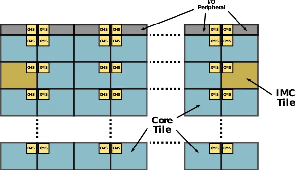
Below is the general floorplan.
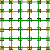
Tiles are replicated in the X and Y axis as many times as desired. The type of tile depends on the design goals and target market. In theory any type of IP block can serve as a tile provided it's modified to interface with the CMS. Each tile is associated with its own CMS which allows the tile to interface with the mesh. Every mesh stop at each tile is directly connected to its immediate four neighbors – north, south, east, and west.
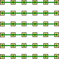
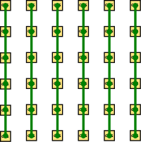
The mesh itself consists of a 2-dimensional array of half-rings. Every vertical column of CMSs form a bi-directional half ring. Similarly, every horizontal row forms a bi-directional half ring.
Operations[edit]
A packet follows a simple routing algorithm:
- Packets are 1st routed vertically
- Packets are then routed horizontally
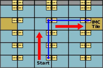
A packet originates at a tile (e.g. from the CHA) or some an I/O peripheral. It enters the fabric at its local Mesh Stop (CMS). The packet is then routed along the vertical half ring, either north or south, always taking the shortest path. Once the packet reaches its destination row, it will be taken off the vertical half ring and placed on the horizontal half ring where it will continue to the destination tile. Once the packet reaches the destination tile, it will interface back with the tile via Mesh Stop.
Example[edit]
Consider the 5 by 6 example mesh below. For a packet to go from the tile labeled 'Start' to the IMC, the packet will leave the core via the CHA and onto the mesh via the CMS. The packet will then be routed through three stops going north. The packet will then be taken off the vertical half ring and placed on the horizontal half ring where it will continue three additional stops going east to the IMC.
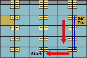
It's important to note that the return path may not be the same route as before. For example, as in this situation, a response from the IMC will be routed via the vertical half ring first to the very south-east corner tile. The packet will then be taken off the vertical half ring and placed on the horizontal half ring where it will go west until it reaches the destination tile.
Cluster Modes[edit]
Intel supports a number of different cluster modes with the mesh interconnect. Note that not all modes are supported by all microarchitectures.
- All-to-all
- Quadrant
- Sub-NUMA
Implementations[edit]
Knights Landing[edit]
- Main article: Knights Landing
The Xeon Phi many-core processors based on the Knights Landing microarchitecture were the first ones to utilize the mesh interconnect. In the case of Knights Landing, a tile actually consisted of a core duplex. The die was arranged as 7 rows by 6 columns for a total of 42 tiles. Two of the tiles are used for I/O while two additional tiles are for the IMC tiles, leaving a total of 38 core tiles (note that 2 tiles are disabled).
Skylake (server)[edit]
- Main article: Skylake (server)
The first Intel server and HEDT microprocessors to implement the mesh were those based on the Skylake server configuration. Skylake came in three different die configurations.
- 12 tiles (3x4), 10-core, Low Core Count (LCC)
- 20 tiles (5x4), 18-core, High Core Count (HCC)
- 30 tiles (5x6), 28-core, Extreme Core Count (XCC)
In every configuration, there are two core tiles removed and replaced by two IMC tile on both edges of the die.
References[edit]
- Some information was obtained directly from Intel
- IEEE Hot Chips 27 Symposium (HCS) 2015.
- IEEE ISSCC 2018
