| Edit Values | |
| FT1 | |
| General Info | |
| Designer | AMD |
| Introduction | January 4, 2011 (launched) |
| Market | Mobile, Embedded |
| Microarchitecture | Bobcat |
| TDP | 18 W 18,000 mW 0.0241 hp 0.018 kW |
| Package | |
| Name | FT1, UOB413 |
| Type | FC-OBGA |
| Contacts | 413 |
| Dimension | 19.0 mm 1.9 cm × 19.0 mm0.748 in 1.9 cm × 1.92 mm0.748 in 0.0756 in |
| Pitch | 0.8 mm 0.0315 in |
FT1 was a CPU package for low power AMD microprocessors with integrated graphics targeting the thin client, embedded, and tablet market, the successor to the ASB2 package. Its counterparts for the mainstream mobile and desktop markets are Socket FS1 and Socket FM1 respectively. FT1 was superseded by the FT3 package.
Package FT1 was used in AMD's "Brazos" platform for ultrathin notebooks. All processors in the FT1 package are members of AMD's x86 CPU Family 14h with CPU cores based on the Bobcat microarchitecture, and were manufactured on a TSMC 40 nm bulk CMOS process.
Contents
Features
- Lidless ball grid array package, 19.0 mm × 19.0 mm × 1.92 mm
- 413 contacts, 0.8 - 1.0 mm multi-pitch
- Organic substrate, flip chip die attachment
- 1 × 64 bit DDR3 SDRAM interface
- Up to 667 MHz, PC3-10600 (DDR3-1333), 10.67 GB/s raw bandwidth
- Up to 2 DIMMs
- UDIMM, SODIMM, or soldered DRAMs
- JEDEC 1.5V, 1.35V
- No ECC support
- PCIe Gen 1, 2 (5 GT/s) from one 5-port, 8-lane controller
- Configurable x4 General Purpose Ports (4x1, 2x2, 1x2 + 2x1, 1x4)
- x4 Unified Media Interface to FCH
- Two independent display controllers
- 2 × DisplayPort 1.1a, up to 2560 × 1600 at 60 Hz, 30 bpp
- 1 × eDP up to 2048 × 1536, 24 bpp, with ext. components
- 1 × LVDS up to 1440 × 900 or 1400 × 1050 at 60 Hz, 18 bpp
- 1 × VGA up to 2560 × 1600, 400 MHz
- 2 × SL DVI up to 1920 × 1200 at 60 Hz, 24 bpp, with ext. components
- 1 × HDMI up to 1920 × 1080 at 60 Hz, 36 bpp, with ext. components
Chipsets
- AMD FCH A50M "Hudson-M1"
- AMD FCH A55E "Hudson-E1"
The chipset is attached with an x4 UMI link (A50M PCIe Gen 1 (2.5 GT/s), A55E Gen 2) and can provide the following additional interfaces:
- 4 lanes PCIe Gen 1, 2 (5 GT/s) configurable x4/x2/x1
- 32-bit, 33 MHz PCI, max. four slots (A55E only)
- 6 × SATA Gen 1, 2, 3 (6 Gb/s)
- 14 × USB 1.1, 2.0
- 2 × USB 1.1
- Gb Ethernet MAC (A55E only)
- HDA, LPC, SPI, SMBus, GPIO
Processors using package FT1
- AMD C-Series "Ontario" (9 W)
- AMD E-Series "Zacate" (18 W)
- AMD Embedded G-Series "eBrazos"
- AMD Z-Series "Desna" (< 6 W)
| CPU | GPU | ||||||||
|---|---|---|---|---|---|---|---|---|---|
| Model | Family | Cores | L2$ | Frequ. | Brand | Frequ. | TDP | Launched | OPN |
| T16R | Embedded G-Series | 1 | 512 KiB 0.5 MiB 524,288 B 4.882812e-4 GiB | 615 MHz 0.615 GHz 615,000 kHz | Radeon HD 6250 | 276 MHz 0.276 GHz 276,000 KHz | 4.5 W 4,500 mW 0.00603 hp 0.0045 kW | June 2012 | GET16RFWB12GVE |
| T24L | Embedded G-Series | 1 | 512 KiB 0.5 MiB 524,288 B 4.882812e-4 GiB | 1,000 MHz 1 GHz 1,000,000 kHz | 5 W 5,000 mW 0.00671 hp 0.005 kW | 1 March 2011 | GET24LFQB12GVE | ||
| T30L | Embedded G-Series | 1 | 512 KiB 0.5 MiB 524,288 B 4.882812e-4 GiB | 1,400 MHz 1.4 GHz 1,400,000 kHz | 18 W 18,000 mW 0.0241 hp 0.018 kW | 1 March 2011 | GET30LGBB12GVE | ||
| T40E | Embedded G-Series | 2 | 1,024 KiB 1 MiB 1,048,576 B 9.765625e-4 GiB | 1,000 MHz 1 GHz 1,000,000 kHz | Radeon HD 6250 | 280 MHz 0.28 GHz 280,000 KHz | 6.4 W 6,400 mW 0.00858 hp 0.0064 kW | 23 May 2011 | GET40EFSB22GVE |
| T40N | Embedded G-Series | 2 | 1,024 KiB 1 MiB 1,048,576 B 9.765625e-4 GiB | 1,000 MHz 1 GHz 1,000,000 kHz | Radeon HD 6290 | 280 MHz 0.28 GHz 280,000 KHz | 18 W 18,000 mW 0.0241 hp 0.018 kW | 19 January 2011 | GET40NFPB22GVE |
| T40R | Embedded G-Series | 1 | 512 KiB 0.5 MiB 524,288 B 4.882812e-4 GiB | 1,000 MHz 1 GHz 1,000,000 kHz | Radeon HD 6250 | 280 MHz 0.28 GHz 280,000 KHz | 5.5 W 5,500 mW 0.00738 hp 0.0055 kW | 23 May 2011 | GET40RFSB12GVE |
| T44R | Embedded G-Series | 1 | 512 KiB 0.5 MiB 524,288 B 4.882812e-4 GiB | 1,200 MHz 1.2 GHz 1,200,000 kHz | Radeon HD 6250 | 280 MHz 0.28 GHz 280,000 KHz | 9 W 9,000 mW 0.0121 hp 0.009 kW | 19 January 2011 | GET44RFPB12GVE |
| T48E | Embedded G-Series | 2 | 1,024 KiB 1 MiB 1,048,576 B 9.765625e-4 GiB | 1,400 MHz 1.4 GHz 1,400,000 kHz | Radeon HD 6250 | 280 MHz 0.28 GHz 280,000 KHz | 18 W 18,000 mW 0.0241 hp 0.018 kW | 2012 | GET48EGBB22GVE |
| T48L | Embedded G-Series | 2 | 1,024 KiB 1 MiB 1,048,576 B 9.765625e-4 GiB | 1,400 MHz 1.4 GHz 1,400,000 kHz | 18 W 18,000 mW 0.0241 hp 0.018 kW | 1 March 2011 | GET48LGBB22GVE | ||
| T48N | Embedded G-Series | 2 | 1,024 KiB 1 MiB 1,048,576 B 9.765625e-4 GiB | 1,400 MHz 1.4 GHz 1,400,000 kHz | Radeon HD 6310 | 520 MHz 0.52 GHz 520,000 KHz | 18 W 18,000 mW 0.0241 hp 0.018 kW | 19 January 2011 | GET48NGBB22GVE |
| T52R | Embedded G-Series | 1 | 512 KiB 0.5 MiB 524,288 B 4.882812e-4 GiB | 1,500 MHz 1.5 GHz 1,500,000 kHz | Radeon HD 6310 | 500 MHz 0.5 GHz 500,000 KHz | 18 W 18,000 mW 0.0241 hp 0.018 kW | 19 January 2011 | GET52RGBB12GVE |
| T56E | Embedded G-Series | 2 | 1,024 KiB 1 MiB 1,048,576 B 9.765625e-4 GiB | 1,650 MHz 1.65 GHz 1,650,000 kHz | Radeon HD 6250 | 275 MHz 0.275 GHz 275,000 KHz | 18 W 18,000 mW 0.0241 hp 0.018 kW | 2012 | GET56EGBB22GVE |
| T56N | Embedded G-Series | 2 | 1,024 KiB 1 MiB 1,048,576 B 9.765625e-4 GiB | 1,650 MHz 1.65 GHz 1,650,000 kHz | Radeon HD 6320 | 500 MHz 0.5 GHz 500,000 KHz | 18 W 18,000 mW 0.0241 hp 0.018 kW | 19 January 2011 | GET56NGBB22GVE |
| Count: 13 | |||||||||
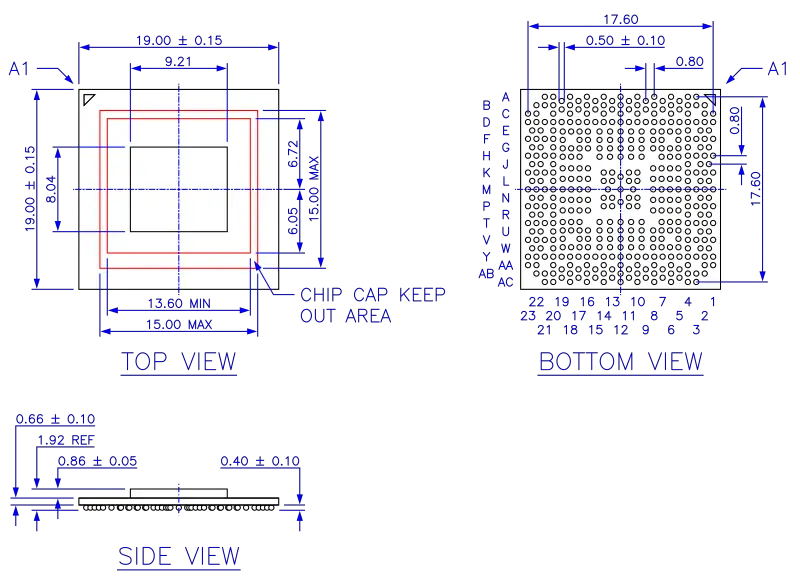
Package Diagram
All dimensions in millimeters.
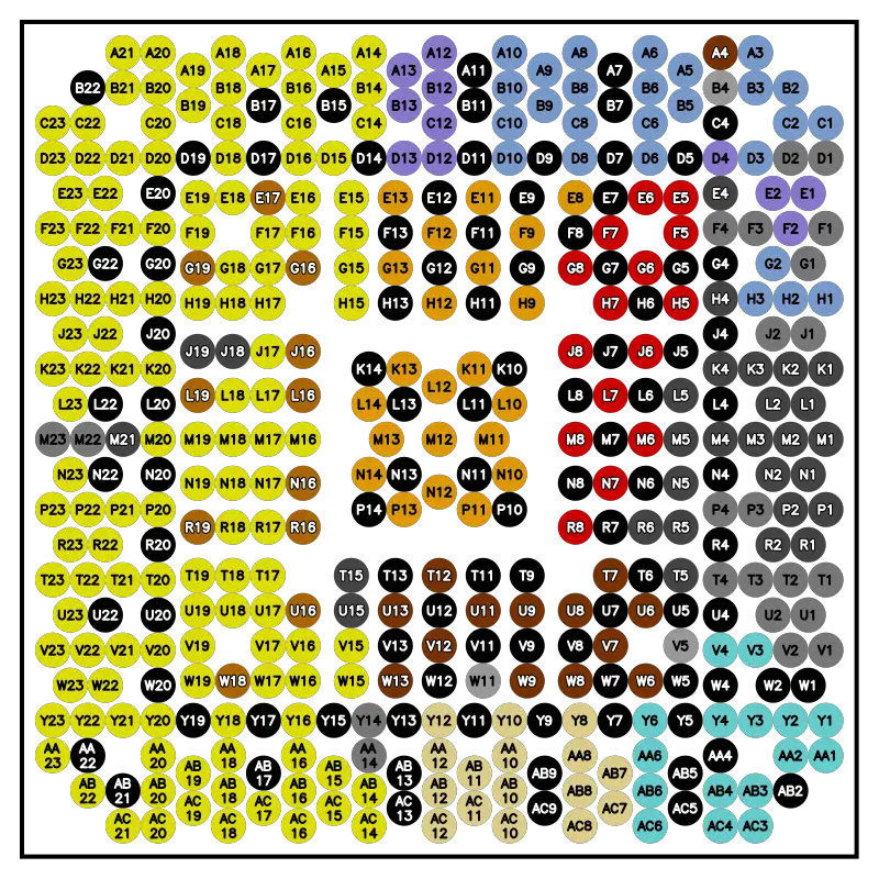
FT1 package ball numbers.
Pin Map
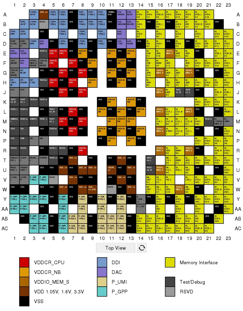
FT1 pinout.
Pin Description
| Signal | Type | Description |
|---|---|---|
| M_ADD[15:0] | O-IO-S | DRAM Column/Row Address |
| M_BANK[2:0] | O-IO-S | DRAM Bank Address |
| M_CAS_L | O-IO-S | DRAM Column Address Strobe |
| M_CKE[1:0] | O-IO-S | DRAM Clock Enable |
| M_CLK_H/L[3:0] | O-IO-S | DRAM Differential Clock |
| M_DATA[63:0] | B-IO-S | DRAM Data Bus |
| M_DM[7:0] | O-IO-S | DRAM Data Mask |
| M_DQS_H/L[7:0] | B-IO-D | DRAM Differential Data Strobe |
| M_EVENT_L | I-IO-S | DRAM Thermal Event |
| M_RAS_L | O-IO-S | DRAM Row Address Strobe |
| M_RESET_L | O-IO-S | DRAM Reset Pin for Suspend-to-RAM Power Management Mode |
| M_VREF | VREF | Memory Interface Voltage Reference |
| M_WE_L | O-IO-S | DRAM Write Enable |
| M0_CS_L[1:0], M1_CS_L[1:0] | O-IO-S | DRAM Chip Selects |
| M0_ODT[1:0], M1_ODT[1:0] | O-IO-S | DRAM Enable Pin for On Die Termination |
| M_ZVDDIO_MEM_S | A | DRAM Interface Drive-Strength Compensation Resistor to VDDIO |
| P_GPP_RXP/RXN[3:0] | I-PCIe-D | General Purpose External PCIe Receive Data Differential Pairs |
| P_GPP_TXP/TXN[3:0] | O-PCIe-D | General Purpose External PCIe Transmit Data Differential Pairs |
| P_UMI_RXP/RXN[3:0] | I-PCIe-D | Unified Media Interface Receive Data Differential Pairs |
| P_UMI_TXP/TXN[3:0] | O-PCIe-D | Unified Media Interface Transmit Data Differential Pairs |
| P_ZVDD_10 | A | PCIe Drive-Strength Compensation Resistor to P_VDD_10 Power Supply |
| P_ZVSS | A | PCIe Drive-Strength Compensation Resistor to VSS |
| LTDP0_TXP/TXN[3:0] | O-PCIe-D | LVDS/TMDS DisplayPort 0 Differential Transmitter |
| TDP1_TXP/TXN[3:0] | O-PCIe-D | TMDS DisplayPort 1 Differential Transmitter |
| LTDP0/TDP1_AUXP/AUXN | B-IO33-D | DisplayPort Auxiliary Channel |
| LTDP0/TDP1_HPD | I-IO33-S | DisplayPort Hot Plug Detect |
| DP_BLON | O-IO33-S | Display Panel Backlight Enable |
| DP_DIGON | O-IO33-S | Display Panel Power Enable |
| DP_VARY_BL | O-IO33-S | Display Backlight Brightness Control |
| DP_ZVSS | A | DP Drive-Strength Compensation Resistor to VSS |
| DAC_RED, DAC_REDB | A | Red for Video Monitor Output |
| DAC_GREEN, DAC_GREENB | A | Green for Video Monitor Output |
| DAC_BLUE, DAC_BLUEB | A | Blue for Video Monitor Output |
| DAC_HSYNC, DAC_VSYNC | O-IO33-S | Display Horizontal, Vertical Sync |
| DAC_SCL | O-IO33-OD | I2C Clock for Display (to video monitor) |
| DAC_SDA | B-IO33-OD | I2C Data for Display |
| DAC_ZVSS | A | DAC Drive-Strength Compensation Resistor to DAC Ground Pin |
| CLKIN_H/L | I-IO18-D | 100 MHz PLL Differential Reference Clock |
| DISP_CLKIN_H/L | I-IO18-D | 100 MHz Display Controller Reference Clock |
| DMAACTIVE_L | I-IO18-S | Indicated System DMA Activity |
| PWROK | I-IO18-S | Voltages and CLKIN have reached specified operation |
| RESET_L | I-IO18-S | Processor Reset |
| ALERT_L | O-IO33-OD | Programmable pin that can indicate different events, including a SB-TSI interrupt |
| PROCHOT_L | B-IO33-OD | Processor in HTC-active state |
| SIC | I-IO33-S | Sideband Interface (SB-TSI) Clock |
| SID | B-IO33-OD | Sideband Interface Data |
| THERMTRIP_L | O-IO33-OD | Thermal Sensor Trip Output |
| DBREQ_L | I-IO18-S | Debug Request |
| DBRDY | O-IO18-S | Debug Ready |
| TCK | I-IO18-S | JTAG Clock |
| TDI | I-IO18-S | JTAG Data Input |
| TDO | O-IO18-S | JTAG Data Output |
| TMS | I-IO18-S | JTAG Mode Select |
| TRST_L | I-IO18-S | JTAG Reset |
| TEST* | Test signal | |
| SVC | O-IO18-S | Serial VID Interface Clock |
| SVD | B-IO18-OD | Serial VID Interface Data |
| VDDCR_CPU | S | Core Power Supply |
| VDDCR_CPU_SENSE | A | VDDCR_CPU Voltage Monitor Pin |
| VDDCR_NB | S | Northbridge Power Supply |
| VDDCR_NB_SENSE | A | VDDCR_NB Voltage Monitor Pin |
| VDDIO_MEM_S | S | DRAM I/O Ring Power Supply |
| VDDIO_MEM_S_SENSE | A | VDDIO_MEM_S Voltage Monitor Pin |
| VDD_10 | S | 1.05 V Supply Pins |
| VDDPL_10 | S | 1.05 V Supply Pin for System PLL |
| VDD_18 | S | 1.8 V Supply Pins |
| VDD_18_DAC | S | 1.8 V Supply Pin for DAC |
| VDD_33 | S | 3.3 V Supply Pin |
| VSS | S | Ground |
| VSS_SENSE | A | VSS Voltage Monitor Pin |
| VSSBG_DAC | S | DAC Ground |
| RSVD | Reserved |
Pin Types
| I/O-PCIe-D | Input / Output, PCIe Voltage Domain, Differential |
| I/O/B-IO-D/S/OD | Input / Output / Bidirectional, VDDIO_MEM_S, Differential / Single-Ended / Open Drain |
| I/O/B-IO18-D/S/OD | Input / Output / Bidirectional, VDD_18, Differential / Single-Ended / Open Drain |
| I/O/B-IO33-D/S/OD | Input / Output / Bidirectional, VDD_33, Differential / Single-Ended / Open Drain |
| A | Analog |
| S | Supply Voltage |
Bibliography
- "FT1 Processor Functional Data Sheet", AMD Publ. #44444, Rev. 2.05, November 2010
- "BIOS and Kernel Developer’s Guide (BKDG) for AMD Family 14h Models 00h-0Fh Processors", AMD Publ. #43170, Rev. 3.13, February 17, 2012
- "Revision Guide for AMD Family 14h Models 00h-0Fh Processors", AMD Publ. #47534, Rev. 3.18, February 26, 2013
See also
| designer | AMD + |
| first launched | January 4, 2011 + |
| instance of | package + |
| market segment | Mobile + and Embedded + |
| microarchitecture | Bobcat + |
| name | FT1 + |
| package | FT1 + and UOB413 + |
| package contacts | 413 + |
| package height | 1.92 mm (0.0756 in) + |
| package length | 19 mm (1.9 cm, 0.748 in) + |
| package pitch | 0.8 mm (0.0315 in) + |
| package type | FC-OBGA + |
| package width | 19 mm (1.9 cm, 0.748 in) + |
| tdp | 18 W (18,000 mW, 0.0241 hp, 0.018 kW) + |


