(Aarch32 support was dropped) |
|||
| (55 intermediate revisions by 5 users not shown) | |||
| Line 3: | Line 3: | ||
|atype=CPU | |atype=CPU | ||
|name=Vulcan | |name=Vulcan | ||
| − | |designer= | + | |designer=Broadcom |
|designer 2=Cavium | |designer 2=Cavium | ||
|manufacturer=TSMC | |manufacturer=TSMC | ||
| Line 24: | Line 24: | ||
|isa=ARMv8.1 | |isa=ARMv8.1 | ||
|extension=NEON | |extension=NEON | ||
| + | |extension 2=TrustZone | ||
|l1i=32 KiB | |l1i=32 KiB | ||
|l1i per=core | |l1i per=core | ||
| Line 35: | Line 36: | ||
|l3=1 MiB | |l3=1 MiB | ||
|l3 per=core | |l3 per=core | ||
| + | |predecessor=XLP II | ||
| + | |predecessor link=broadcom/microarchitectures/larrabee | ||
| + | |successor=Triton | ||
| + | |successor link=cavium/microarchitectures/triton | ||
}} | }} | ||
| − | '''Vulcan''' is a [[16 nm]] high-performance {{arch|64}} [[ARM]] microarchitecture designed by [[Broadcom]] and later [[Cavium]] for the server market. | + | '''Vulcan''' is a [[16 nm]] high-performance {{arch|64}} [[ARM]] microarchitecture designed by [[Broadcom]] and later introduced by [[Cavium]] for the server market. |
Introduced in [[2018]], Vulcan-based microprocessors are branded as part of the {{cavium|ThunderX2}} family. | Introduced in [[2018]], Vulcan-based microprocessors are branded as part of the {{cavium|ThunderX2}} family. | ||
| + | |||
| + | == History == | ||
| + | Vulcan can trace its roots all the way back to [[Raza Microelectronics]] {{raza|XLR}} family of [[MIPS]] processors from [[2006]]. With the introduction of their {{raza|XLR}} family in [[2009]], Raza (and later [[NetLogic]]) moved to a high-performance superscalar design with fine-grained 4-way multithreading support. In [[2011]], [[Broadcom]] acquired [[NetLogic Microsystems]] and integrated them into Broadcom's Embedded Processor Group. | ||
| + | |||
| + | In [[2013]], Broadcom announced that they have licensed the ARMv7 and ARMv8 ISAs, allowing them to develop their own micro-architectures based on the ISA. Vulcan is the outcome of this effort which involved adapting the existing core to the [[ARM]] ISA instead of [[MIPS]] and enhancing the cores in various ways. Vulcan development started in early [[2012]] and was expected to enter mass production in mid-[[2015]]. | ||
| + | |||
| + | In [[2016]] [[Cavium]] acquired Vulcan from Broadcom which was introduced the following year. In early [[2018]], Vulcan-based microprocessor entered general availability under the {{cavium|ThunderX2}} brand. | ||
| + | |||
| + | == Brands == | ||
| + | Vulcan is sold under a single brand. | ||
| + | |||
| + | {| class="wikitable" style="text-align: center;" | ||
| + | |- | ||
| + | ! Logo !! Family !! SMP !! SMT !! Cores | ||
| + | |- | ||
| + | | [[File:ThunderX2_logo.png|100px|link=cavium/thunderx2]] || {{cavium|ThunderX2}} || {{tchk|yes|2-way}} || {{tchk|yes|4-way}} || 16-32 | ||
| + | |} | ||
| + | |||
| + | == Release Dates == | ||
| + | Cavium introduced the {{cavium|ThunderX2}} family based on the Vulcan microarchitecture in early 2017. On May 7, 2018, Cavium has announced that they have reached general availability. | ||
| + | |||
| + | == Compiler support == | ||
| + | {| class="wikitable" | ||
| + | ! Compiler !! Arch-Specific !! Arch-Favorable | ||
| + | |- | ||
| + | | GCC || <code>-march=thunderx2t99</code> || <code>-mtune=thunderx2t99</code> | ||
| + | |- | ||
| + | | LLVM || <code>-march=thunderx2t99</code> || <code>-mtune=thunderx2t99</code> | ||
| + | |} | ||
| + | |||
| + | Note that for earlier compiler version (prior to the compiler changes in early 2017), the two compilers used the actual Vulcan name as the option. | ||
| + | |||
| + | {| class="wikitable" | ||
| + | ! Compiler !! Arch-Specific !! Arch-Favorable !! Patched Change | ||
| + | |- | ||
| + | | GCC || <code>-march=vulcan</code> || <code>-mtune=vulcan</code> || [https://reviews.llvm.org/D30510 Change D30510] | ||
| + | |- | ||
| + | | LLVM || <code>-march=vulcan</code> || <code>-mtune=vulcan</code> || [https://bugs.llvm.org/show_bug.cgi?id=32113 Chnage 32113] | ||
| + | |} | ||
== Architecture == | == Architecture == | ||
| − | {{ | + | Vulcan builds on the prior MIPS-based {{broadcom|XLP II|l=arch}} microarchitecture. The design has been substantially improved and changed to execute [[ARM]] (based on the [[ARMv8.1]] ISA). |
| + | |||
| + | === Key changes from {{broadcom|XLP II|l=arch}} === | ||
| + | * Converted to [[ARM]] ISA (from [[MIPS]]) | ||
| + | ** Aarch64 | ||
| + | * [[16 nm lithography process|16nm FinFET process]] (from [[28 nm|28 nm planar]]) | ||
| + | * 40% IPC improvement | ||
| + | * 25% higher [[clock]] (2.5 GHz, up from 2 GHz) | ||
| + | * Core | ||
| + | ** Longer pipeline (15 stages, up from 13) | ||
| + | ** Improved branch predictor | ||
| + | ** Double fetch throughput (4, up from 2) | ||
| + | ** New Decoder | ||
| + | *** Decodes ARMv8.1 (Instead of MIPS64 R5) | ||
| + | *** Decodes to [[micro-ops]] | ||
| + | **** Roughly 10-20% more µOPs | ||
| + | ** New loop buffer | ||
| + | ** Execution Engine | ||
| + | *** New scheduler | ||
| + | **** Unified schedule (from distributed) | ||
| + | ***** 60 entries | ||
| + | *** Large ROB (180 entries, up from 100) | ||
| + | *** Execution Units | ||
| + | **** New FP Unit (2, up from 1) | ||
| + | **** Wider FP Units (128-bit, up from 64-bit) | ||
| + | ** Memory Subsystem | ||
| + | *** Double load bandwidth (128-bit, up from 64-bit) | ||
| + | *** New Store Data Unit | ||
| + | *** Half L2 Cache Size (256 KiB, down form 512 KiB) | ||
| + | * Memory Controller | ||
| + | ** DDR3 '''→''' DDR4 | ||
| + | ** 4 '''→''' 8 channels | ||
| + | ** 1600 MT/s '''→''' 2666 MT/s | ||
| + | ** 47.68 GiB/s '''→''' 158.9 GiB/s | ||
=== Block Diagram === | === Block Diagram === | ||
| − | + | ==== Entire Chip ==== | |
| + | |||
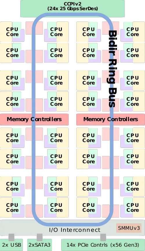
| + | :[[File:vulcan chip block diagram.svg|500px]] | ||
| + | |||
| + | ==== Individual Core ==== | ||
| + | |||
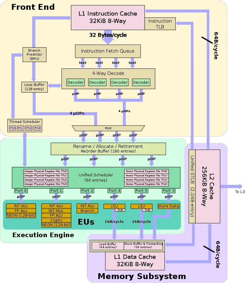
| + | :[[File:vulcan block diagram.svg|800px]] | ||
=== Memory Hierarchy === | === Memory Hierarchy === | ||
| − | + | * Cache | |
| + | ** L1I Cache | ||
| + | *** 32 KiB, 8-way set associative | ||
| + | ** L1D Cache | ||
| + | *** 32 KiB, 8-way set associative | ||
| + | ** L2 Cache | ||
| + | *** 256 KiB, 8-way set associative | ||
| + | ** L3 Cache | ||
| + | *** 16 tiles, line stripped | ||
| + | *** 1 MiB/core slice | ||
| + | *** Shared | ||
| + | *** Exclusive of L2 | ||
| + | **** Victim cache | ||
| + | ** System DRAM | ||
| + | *** 2 TiB Max Memory / socket | ||
| + | *** 8 Channels | ||
| + | *** DDR4, up to 2666 MT/s | ||
| + | **** 1 DPC and 2 DPC support | ||
| + | **** RDIMM, LRDIMM, NVDIMM-P support | ||
| + | **** Single, Dual and Quad rank modules | ||
| + | *** 8 B/cycle/channel (@ memory clock) | ||
| + | *** ECC | ||
| + | * TLBs | ||
| + | ** ITLB | ||
| + | *** Dedicated instruction TLB | ||
| + | *** DTLB | ||
| + | **** TLB unit for each LSU | ||
| + | ** STLB | ||
| + | *** 2048-entry | ||
| + | *** 4 KiB - 16 GiB pages | ||
== Overview == | == Overview == | ||
| − | {{ | + | [[File:vulcan overview.svg|500px|right]] |
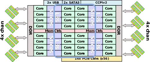
| + | Scaled up from prior architectures in all vectors (performance, area, and [[TDP]]), Vulcan was designed to be a {{intel|Xeon}}-class [[ARM]]-based server microprocessor. Vulcan features 32 high-performance custom-designed [[ARM]] cores fully compliant with [[ARMv8.1]] along with their accompanying 1 MiB of level 3 cache slice (for a total of 32 MiB of shared [[last level cache]]). Since each core supports up to [[simultaneous multithreading|four simultaneous]] threads, the full configuration can support up to 128 threads. Supporting a large number of cores, are eight [[DDR4]] channels capable of data rates of up to 2,666 MT/s, allowing for 170.7 GB/s of aggregated bandwidth. | ||
| + | |||
| + | The processor comes with 14 fully-configurable PCIe Gen3 controllers with 56 available lanes. The chip also has 2 USB 3 and 2 SATA 3 ports. | ||
| + | |||
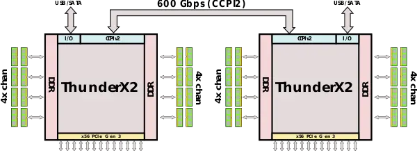
| + | Vulcan supports up to two-way multiprocessing through their second-generation {{cavium|Cavium Coherent Processor Interconnect}} (CCPI2) capable of providing 600 Gbps of aggregated bandwidth. | ||
== Core == | == Core == | ||
| − | {{ | + | Vulcan is an [[out-of-order]] superscalar with support for up to four simultaneous hardware threads. Vulcan features a 13-15-stage pipeline, slightly longer than the XLP II. |
| + | === Front-end === | ||
| + | Vulcan's front-end is tasked with fetching instructions from a ready thread instruction stream and feeding them into the decode in order to be delivered to the execution units. Since Vulcan supports up to four threads, a thread scheduler determines from which thread's instruction stream to operate on. This determination is done on each cycle with the help of the branch predictor with no added cost. | ||
| + | |||
| + | Vulcan has a 32 KiB L1 cache which is 8-way set associative and a dedicate L1 instruction TLB. It's worth noting that all the core caches on Vulcan are 8-way set associative to aid the [[branch predictor]] which works on cache line stride patterns. Under normal flow, the data to be fetched was already predicted and has made it to the L1 from the L2. The bandwidth to the L1 instruction cache is 64 bytes per cycle. | ||
| + | |||
| + | ==== Fetch ==== | ||
| + | [[Instruction fetch]] is done on a 32-byte window or 8 (4-byte) [[ARM]] instructions. This is twice the throughput of the previous architecture and is designed in order to better absorb bubbles in the pipeline. The instruction stream is decomposed into its constituent instructions where they are queued to go for the [[instruction decode|decoder]]. The queue is shared by all threads. The size of the queue has not been disclosed. | ||
| + | |||
| + | ==== Decoding ==== | ||
| + | Each cycle, up to four instructions are sent to the [[instruction decode|decoder]]. In prior design, [[Broadcom]]'s products decoded [[MIPS]] instructions. With Vulcan, the switching to ARM meant the decoder had to be replaced with much more complex logic that decodes the original [[instruction]] and emits [[micro-ops]]. For the most part, there is a 1:1 mapping between instructions and µOP with an average of 15% more µOPs emitted from instructions. The extra complexity has added another pipeline stage to the decode. | ||
| + | ==== Loop Buffer ==== | ||
| + | Sitting between the [[instruction decode|decoder]] and the [[instruction scheduler|scheduler]] is a 128-entry [[loop buffer]]. The loop buffer, in conjunction with the [[branch predictor]], will queue recent tight loop operations. The buffer will play back the operations repeatedly until a branch take occurs. When this takes place, the front-end (instruction fetch, decode, etc..) is largely power-gated in order to save power. | ||
| + | |||
| + | === Execution engine === | ||
| + | Vulcan's back-end handles the execution of out-of-order operations. Vulcan's back-end has been substantially enhanced from prior designs including a complete redesign of the [[instruction scheduler|scheduler]]. Most of the improvements dealt with entirely reworking the scheduler in order to more efficiently extract additional instruction-level parallelism opportunities. From decode, instructions are sent to the [[Reorder Buffer]] (ROB) at the rate of up to 4 µOPs each cycle. | ||
| + | |||
| + | ==== Renaming & Allocation ==== | ||
| + | In the prior XLP II microarchitecture, [[NetLogic]] had a five-queue instruction distributed scheduler mechanism whereby each queue is associated with certain execution units. In Cavium, Broadcom got rid of the distributed scheduler and replaced it with a more efficient unified scheduler, similar in design to Intel's {{intel|Skylake (Client)|Skylake|l=arch}}. | ||
| + | |||
| + | Vulcan's [[Reorder Buffer]] is 180-entry in size, an 80-entry increase over prior design. The ROB tracks all µOPs in flight. Vulcan renames and retires up to 4 µOPs per cycle. | ||
| + | |||
| + | ==== Scheduler ==== | ||
| + | Vulcan uses a 60-entry unified scheduler. Each cycle, up to six µOPs can be issued to the execution units, a much wider design from the four µOPs issue in prior design. It's worth noting that in order to support four threads, Vulcan duplicates most of the logic for each thread such as all the registers, architectural states, program counters, and interrupts. Ready µOPs from any thread are issued on each cycle. | ||
| + | |||
| + | ==== Execution Units ==== | ||
| + | Up to six µOPs can be sent into Vulcan's six execution units each cycle. As far as integer operations, up to three operations can be issued each cycle. One of the ALUs also handles branch instructions. Note that only the ALU on port 1 can perform complex integer operations (i.e., [[multiplication]] and [[division]]) in addition to the simple integer operations. The other two ALUs can only perform simple integer operations. | ||
| + | |||
| + | Vulcan has doubled the number of [[floating point]] units to two and widened them to 128-bit to support [[ARM]]'s {{arm|NEON}} operations (prior design was only 64-bit wide). In theory, Vulcan's peak performance now stands at 8 [[FLOPS]]/cycle or 8 GFLOPS at 1 GHz. | ||
| + | |||
| + | Port 1 has addition support for crypto operations supporting [[ARM]]'s crypto extension (e.g., ARM <code>AES</code>, <code>SHA1</code>, <code>SHA256</code> instructions). | ||
| + | |||
| + | === Memory subsystem === | ||
| + | Vulcan's memory subsystem deals with the loads and store requests and ordering. There are two [[load-store units]] each capable of moving 128-bit of data - double the bandwidth of the XLP II. The widening of the units was done in order to more efficiently support operations such as the Load Pair (<code>LDP</code>) and Store Pair (<code>STP</code>) instructions. In addition to the LSUs, there is a new dedicated Store Address unit. Similar to Intel's older architectures, the store operation is cracked into two distinct operations - a store address operation used to calculate the effective address and finally the store data operation. Vulcan can issue a store to the Store Address unit before the data is available where the address can be calculated and [[memory ordering conflicts]] can be detected. Once the data is ready, the operation will be reissued to the LSU. The [[store buffer]] is 36-entry deep with the [[load buffer]] at 64-entries for a total of 100 [[simultaneous memory operations]] in-flight or roughly 55% of all µOPs. Note that the store buffer is considerably smaller than the load buffer because Vulcan can only sustain a single store operation per cycle as most workloads do far more loads than stores. | ||
| + | |||
| + | Vulcan's L2 cache is 256 KiB, half that of prior design, and has an [[L2]] to [[L1]] bandwidth of 64 bytes per cycle in either direction. There is a 1 MiB L3 cache per core arranged as 2 MiB slices for a total of 32 MiB of cache shared by the entire chip. The L3 is [[exclusive cache]], filling up with evicted L2 cache lines. | ||
| + | |||
| + | ==== Miss sequence ==== | ||
| + | There are 16 tiles of L3 that are cache line stripped. though broken down into slices, there is no notion of L3 cache affinity to the cores. On an L2 miss, a hash is used to determine the home L3 cache hit. A check is done to determine if the cache line is found in that L3 tile and if found, return the data. Cavium implemented an enhanced version of the [[MOESI protocol]]. When not found, a [[snoop filter]] indicates the presence of the data in other cores. If present following a snoop, the owner transfers the line. On negative snoops for all cores, a DRAM request is issued to the memory controller. | ||
| + | |||
| + | == System Architecture == | ||
| + | Vulcan incorporates 32 cores on a single monolithic die. The cores are interconnected using a bidirectional ring bus, meaning the worst case path is halved. It appears that the cores consist of quad-core blocks with the L3 cache being the crossbar between the cores in the block. Eight of those cores are interconnected via the ring which operates at core frequency. The exact behavior has not been disclosed but in the XLP II, the ring was capable of moving 64 bytes of data each cycle per core. | ||
| + | |||
| + | Attached to the ring is 2nd-generation {{cavium|Cavium Coherent Processor Interconnect}} (CCPI2) used to support multiprocessing as well as the I/O subsystem. In its maximum configuration, the die feature 14 PCIe Gen 3 memory controllers supporting up to 56 lanes. Bifurcation is supported for up to 14 x1/x4, 7x8, or 3x16. | ||
| + | |||
| + | == Scalability == | ||
| + | Vulcan has multiprocessing support. Each die comes with 2nd-generation {{cavium|Cavium Coherent Processor Interconnect}} (CCPI2) which incorporates 24 25 Gpbs SerDes for a total aggregated bandwidth of 600 Gbps between the two sockets. | ||
| + | |||
| + | |||
| + | :[[File:vulcan overview-2way.svg|600px]] | ||
| + | |||
| + | |||
| + | In this configuration, a max system consists of two chips for a total of 64 cores, 256 threads, 16 memory channels and 32 DIMMs, 112 PCIe Gen 3 lanes, 4 SATA3 ports, 4 USB 3 ports, and other various low speed I/O interfaces. | ||
== Die == | == Die == | ||
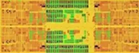
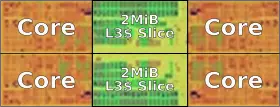
| − | * Broadcom's original die size was around 600 mm². It's unknown how much the die has changed when it was modified by Cavium. | + | === Core Group === |
| + | :[[File:cavium vulcan die core cluster.png|400px]] | ||
| + | |||
| + | |||
| + | :[[File:cavium vulcan die core cluster (annotated).png|400px]] | ||
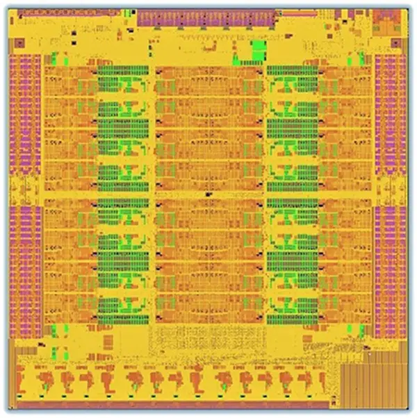
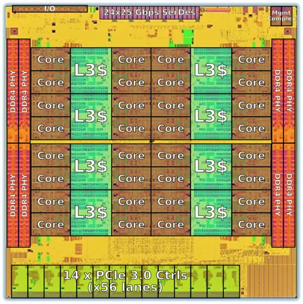
| + | === SoC === | ||
| + | * Broadcom's original die size was rumored to be around 600 mm². It's unknown how much the die has changed when it was modified by Cavium. | ||
* TSMC's [[16 nm process]] | * TSMC's [[16 nm process]] | ||
| + | * 32 cores | ||
| Line 66: | Line 242: | ||
== All Vulcan Chips == | == All Vulcan Chips == | ||
| − | {{ | + | <!-- NOTE: |
| + | This table is generated automatically from the data in the actual articles. | ||
| + | If a microprocessor is missing from the list, an appropriate article for it needs to be | ||
| + | created and tagged accordingly. | ||
| + | |||
| + | Missing a chip? please dump its name here: https://en.wikichip.org/wiki/WikiChip:wanted_chips | ||
| + | --> | ||
| + | {{comp table start}} | ||
| + | <table class="comptable sortable tc4"> | ||
| + | {{comp table header|main|5:List of Vulcan-based Processors}} | ||
| + | {{comp table header|main|5:Main processor}} | ||
| + | {{comp table header|cols|Launched|Cores|Threads|%Frequency|PCIe Lanes}} | ||
| + | {{#ask: [[Category:microprocessor models by cavium]] [[microarchitecture::Vulcan]] | ||
| + | |?full page name | ||
| + | |?model number | ||
| + | |?first launched | ||
| + | |?core count | ||
| + | |?thread count | ||
| + | |?base frequency#GHz | ||
| + | |?Has subobject.max pcie lanes | ||
| + | |format=template | ||
| + | |template=proc table 3 | ||
| + | |userparam=7 | ||
| + | |mainlabel=- | ||
| + | |valuesep=, | ||
| + | }} | ||
| + | {{comp table count|ask=[[Category:microprocessor models by cavium]] [[microarchitecture::Vulcan]]}} | ||
| + | </table> | ||
| + | {{comp table end}} | ||
| − | == | + | == Bibliography == |
| − | * | + | * Broadcom, personal communication, March, 2017 |
| − | * '' | + | * Cavium, personal communication, June, 2018 |
| + | * Cavium Booth No: E–1000 (2018, June). "ThunderX2 Processor Family". ISC 2018, Frankfurt, Germany. | ||
| + | * Schor, D (2018, June). ''[https://fuse.wikichip.org/news/1316/a-look-at-caviums-new-high-performance-arm-microprocessors-and-the-isambard-supercomputer/ A Look at Cavium’s New High-Performance ARM Microprocessors and the Isambard Supercomputer]''. | ||
== See also == | == See also == | ||
* Qualcomm's {{qualcomm|Falkor|l=arch}} | * Qualcomm's {{qualcomm|Falkor|l=arch}} | ||
* Intel's {{intel|Skylake (server)|Skylake|l=arch}} | * Intel's {{intel|Skylake (server)|Skylake|l=arch}} | ||
Latest revision as of 21:11, 4 October 2019
| Edit Values | |
| Vulcan µarch | |
| General Info | |
| Arch Type | CPU |
| Designer | Broadcom, Cavium |
| Manufacturer | TSMC |
| Introduction | 2018 |
| Process | 16 nm |
| Core Configs | 16, 20, 24, 28, 30, 32 |
| Pipeline | |
| Type | Superscalar, Superpipeline |
| OoOE | Yes |
| Speculative | Yes |
| Reg Renaming | Yes |
| Stages | 13-15 |
| Decode | 4-way |
| Instructions | |
| ISA | ARMv8.1 |
| Extensions | NEON, TrustZone |
| Cache | |
| L1I Cache | 32 KiB/core 8-way set associative |
| L1D Cache | 32 KiB/core 8-way set associative |
| L2 Cache | 256 KiB/core 8-way set associative |
| L3 Cache | 1 MiB/core |
| Succession | |
Vulcan is a 16 nm high-performance 64-bit ARM microarchitecture designed by Broadcom and later introduced by Cavium for the server market.
Introduced in 2018, Vulcan-based microprocessors are branded as part of the ThunderX2 family.
Contents
History[edit]
Vulcan can trace its roots all the way back to Raza Microelectronics XLR family of MIPS processors from 2006. With the introduction of their XLR family in 2009, Raza (and later NetLogic) moved to a high-performance superscalar design with fine-grained 4-way multithreading support. In 2011, Broadcom acquired NetLogic Microsystems and integrated them into Broadcom's Embedded Processor Group.
In 2013, Broadcom announced that they have licensed the ARMv7 and ARMv8 ISAs, allowing them to develop their own micro-architectures based on the ISA. Vulcan is the outcome of this effort which involved adapting the existing core to the ARM ISA instead of MIPS and enhancing the cores in various ways. Vulcan development started in early 2012 and was expected to enter mass production in mid-2015.
In 2016 Cavium acquired Vulcan from Broadcom which was introduced the following year. In early 2018, Vulcan-based microprocessor entered general availability under the ThunderX2 brand.
Brands[edit]
Vulcan is sold under a single brand.
| Logo | Family | SMP | SMT | Cores |
|---|---|---|---|---|
| |
ThunderX2 | 2-way | 4-way | 16-32 |
Release Dates[edit]
Cavium introduced the ThunderX2 family based on the Vulcan microarchitecture in early 2017. On May 7, 2018, Cavium has announced that they have reached general availability.
Compiler support[edit]
| Compiler | Arch-Specific | Arch-Favorable |
|---|---|---|
| GCC | -march=thunderx2t99 |
-mtune=thunderx2t99
|
| LLVM | -march=thunderx2t99 |
-mtune=thunderx2t99
|
Note that for earlier compiler version (prior to the compiler changes in early 2017), the two compilers used the actual Vulcan name as the option.
| Compiler | Arch-Specific | Arch-Favorable | Patched Change |
|---|---|---|---|
| GCC | -march=vulcan |
-mtune=vulcan |
Change D30510 |
| LLVM | -march=vulcan |
-mtune=vulcan |
Chnage 32113 |
Architecture[edit]
Vulcan builds on the prior MIPS-based XLP II microarchitecture. The design has been substantially improved and changed to execute ARM (based on the ARMv8.1 ISA).
Key changes from XLP II[edit]
- Converted to ARM ISA (from MIPS)
- Aarch64
- 16nm FinFET process (from 28 nm planar)
- 40% IPC improvement
- 25% higher clock (2.5 GHz, up from 2 GHz)
- Core
- Longer pipeline (15 stages, up from 13)
- Improved branch predictor
- Double fetch throughput (4, up from 2)
- New Decoder
- Decodes ARMv8.1 (Instead of MIPS64 R5)
- Decodes to micro-ops
- Roughly 10-20% more µOPs
- New loop buffer
- Execution Engine
- New scheduler
- Unified schedule (from distributed)
- 60 entries
- Unified schedule (from distributed)
- Large ROB (180 entries, up from 100)
- Execution Units
- New FP Unit (2, up from 1)
- Wider FP Units (128-bit, up from 64-bit)
- New scheduler
- Memory Subsystem
- Double load bandwidth (128-bit, up from 64-bit)
- New Store Data Unit
- Half L2 Cache Size (256 KiB, down form 512 KiB)
- Memory Controller
- DDR3 → DDR4
- 4 → 8 channels
- 1600 MT/s → 2666 MT/s
- 47.68 GiB/s → 158.9 GiB/s
Block Diagram[edit]
Entire Chip[edit]
Individual Core[edit]
Memory Hierarchy[edit]
- Cache
- L1I Cache
- 32 KiB, 8-way set associative
- L1D Cache
- 32 KiB, 8-way set associative
- L2 Cache
- 256 KiB, 8-way set associative
- L3 Cache
- 16 tiles, line stripped
- 1 MiB/core slice
- Shared
- Exclusive of L2
- Victim cache
- System DRAM
- 2 TiB Max Memory / socket
- 8 Channels
- DDR4, up to 2666 MT/s
- 1 DPC and 2 DPC support
- RDIMM, LRDIMM, NVDIMM-P support
- Single, Dual and Quad rank modules
- 8 B/cycle/channel (@ memory clock)
- ECC
- L1I Cache
- TLBs
- ITLB
- Dedicated instruction TLB
- DTLB
- TLB unit for each LSU
- STLB
- 2048-entry
- 4 KiB - 16 GiB pages
- ITLB
Overview[edit]
Scaled up from prior architectures in all vectors (performance, area, and TDP), Vulcan was designed to be a Xeon-class ARM-based server microprocessor. Vulcan features 32 high-performance custom-designed ARM cores fully compliant with ARMv8.1 along with their accompanying 1 MiB of level 3 cache slice (for a total of 32 MiB of shared last level cache). Since each core supports up to four simultaneous threads, the full configuration can support up to 128 threads. Supporting a large number of cores, are eight DDR4 channels capable of data rates of up to 2,666 MT/s, allowing for 170.7 GB/s of aggregated bandwidth.
The processor comes with 14 fully-configurable PCIe Gen3 controllers with 56 available lanes. The chip also has 2 USB 3 and 2 SATA 3 ports.
Vulcan supports up to two-way multiprocessing through their second-generation Cavium Coherent Processor Interconnect (CCPI2) capable of providing 600 Gbps of aggregated bandwidth.
Core[edit]
Vulcan is an out-of-order superscalar with support for up to four simultaneous hardware threads. Vulcan features a 13-15-stage pipeline, slightly longer than the XLP II.
Front-end[edit]
Vulcan's front-end is tasked with fetching instructions from a ready thread instruction stream and feeding them into the decode in order to be delivered to the execution units. Since Vulcan supports up to four threads, a thread scheduler determines from which thread's instruction stream to operate on. This determination is done on each cycle with the help of the branch predictor with no added cost.
Vulcan has a 32 KiB L1 cache which is 8-way set associative and a dedicate L1 instruction TLB. It's worth noting that all the core caches on Vulcan are 8-way set associative to aid the branch predictor which works on cache line stride patterns. Under normal flow, the data to be fetched was already predicted and has made it to the L1 from the L2. The bandwidth to the L1 instruction cache is 64 bytes per cycle.
Fetch[edit]
Instruction fetch is done on a 32-byte window or 8 (4-byte) ARM instructions. This is twice the throughput of the previous architecture and is designed in order to better absorb bubbles in the pipeline. The instruction stream is decomposed into its constituent instructions where they are queued to go for the decoder. The queue is shared by all threads. The size of the queue has not been disclosed.
Decoding[edit]
Each cycle, up to four instructions are sent to the decoder. In prior design, Broadcom's products decoded MIPS instructions. With Vulcan, the switching to ARM meant the decoder had to be replaced with much more complex logic that decodes the original instruction and emits micro-ops. For the most part, there is a 1:1 mapping between instructions and µOP with an average of 15% more µOPs emitted from instructions. The extra complexity has added another pipeline stage to the decode.
Loop Buffer[edit]
Sitting between the decoder and the scheduler is a 128-entry loop buffer. The loop buffer, in conjunction with the branch predictor, will queue recent tight loop operations. The buffer will play back the operations repeatedly until a branch take occurs. When this takes place, the front-end (instruction fetch, decode, etc..) is largely power-gated in order to save power.
Execution engine[edit]
Vulcan's back-end handles the execution of out-of-order operations. Vulcan's back-end has been substantially enhanced from prior designs including a complete redesign of the scheduler. Most of the improvements dealt with entirely reworking the scheduler in order to more efficiently extract additional instruction-level parallelism opportunities. From decode, instructions are sent to the Reorder Buffer (ROB) at the rate of up to 4 µOPs each cycle.
Renaming & Allocation[edit]
In the prior XLP II microarchitecture, NetLogic had a five-queue instruction distributed scheduler mechanism whereby each queue is associated with certain execution units. In Cavium, Broadcom got rid of the distributed scheduler and replaced it with a more efficient unified scheduler, similar in design to Intel's Skylake.
Vulcan's Reorder Buffer is 180-entry in size, an 80-entry increase over prior design. The ROB tracks all µOPs in flight. Vulcan renames and retires up to 4 µOPs per cycle.
Scheduler[edit]
Vulcan uses a 60-entry unified scheduler. Each cycle, up to six µOPs can be issued to the execution units, a much wider design from the four µOPs issue in prior design. It's worth noting that in order to support four threads, Vulcan duplicates most of the logic for each thread such as all the registers, architectural states, program counters, and interrupts. Ready µOPs from any thread are issued on each cycle.
Execution Units[edit]
Up to six µOPs can be sent into Vulcan's six execution units each cycle. As far as integer operations, up to three operations can be issued each cycle. One of the ALUs also handles branch instructions. Note that only the ALU on port 1 can perform complex integer operations (i.e., multiplication and division) in addition to the simple integer operations. The other two ALUs can only perform simple integer operations.
Vulcan has doubled the number of floating point units to two and widened them to 128-bit to support ARM's NEON operations (prior design was only 64-bit wide). In theory, Vulcan's peak performance now stands at 8 FLOPS/cycle or 8 GFLOPS at 1 GHz.
Port 1 has addition support for crypto operations supporting ARM's crypto extension (e.g., ARM AES, SHA1, SHA256 instructions).
Memory subsystem[edit]
Vulcan's memory subsystem deals with the loads and store requests and ordering. There are two load-store units each capable of moving 128-bit of data - double the bandwidth of the XLP II. The widening of the units was done in order to more efficiently support operations such as the Load Pair (LDP) and Store Pair (STP) instructions. In addition to the LSUs, there is a new dedicated Store Address unit. Similar to Intel's older architectures, the store operation is cracked into two distinct operations - a store address operation used to calculate the effective address and finally the store data operation. Vulcan can issue a store to the Store Address unit before the data is available where the address can be calculated and memory ordering conflicts can be detected. Once the data is ready, the operation will be reissued to the LSU. The store buffer is 36-entry deep with the load buffer at 64-entries for a total of 100 simultaneous memory operations in-flight or roughly 55% of all µOPs. Note that the store buffer is considerably smaller than the load buffer because Vulcan can only sustain a single store operation per cycle as most workloads do far more loads than stores.
Vulcan's L2 cache is 256 KiB, half that of prior design, and has an L2 to L1 bandwidth of 64 bytes per cycle in either direction. There is a 1 MiB L3 cache per core arranged as 2 MiB slices for a total of 32 MiB of cache shared by the entire chip. The L3 is exclusive cache, filling up with evicted L2 cache lines.
Miss sequence[edit]
There are 16 tiles of L3 that are cache line stripped. though broken down into slices, there is no notion of L3 cache affinity to the cores. On an L2 miss, a hash is used to determine the home L3 cache hit. A check is done to determine if the cache line is found in that L3 tile and if found, return the data. Cavium implemented an enhanced version of the MOESI protocol. When not found, a snoop filter indicates the presence of the data in other cores. If present following a snoop, the owner transfers the line. On negative snoops for all cores, a DRAM request is issued to the memory controller.
System Architecture[edit]
Vulcan incorporates 32 cores on a single monolithic die. The cores are interconnected using a bidirectional ring bus, meaning the worst case path is halved. It appears that the cores consist of quad-core blocks with the L3 cache being the crossbar between the cores in the block. Eight of those cores are interconnected via the ring which operates at core frequency. The exact behavior has not been disclosed but in the XLP II, the ring was capable of moving 64 bytes of data each cycle per core.
Attached to the ring is 2nd-generation Cavium Coherent Processor Interconnect (CCPI2) used to support multiprocessing as well as the I/O subsystem. In its maximum configuration, the die feature 14 PCIe Gen 3 memory controllers supporting up to 56 lanes. Bifurcation is supported for up to 14 x1/x4, 7x8, or 3x16.
Scalability[edit]
Vulcan has multiprocessing support. Each die comes with 2nd-generation Cavium Coherent Processor Interconnect (CCPI2) which incorporates 24 25 Gpbs SerDes for a total aggregated bandwidth of 600 Gbps between the two sockets.
In this configuration, a max system consists of two chips for a total of 64 cores, 256 threads, 16 memory channels and 32 DIMMs, 112 PCIe Gen 3 lanes, 4 SATA3 ports, 4 USB 3 ports, and other various low speed I/O interfaces.
Die[edit]
Core Group[edit]
SoC[edit]
- Broadcom's original die size was rumored to be around 600 mm². It's unknown how much the die has changed when it was modified by Cavium.
- TSMC's 16 nm process
- 32 cores
All Vulcan Chips[edit]
| List of Vulcan-based Processors | |||||
|---|---|---|---|---|---|
| Main processor | |||||
| Model | Launched | Cores | Threads | Frequency | PCIe Lanes |
| CN9960 | 7 May 2018 | 16 | 64 | 1.6 GHz 1,600 MHz , 1.8 GHz1,600,000 kHz 1,800 MHz , 2 GHz1,800,000 kHz 2,000 MHz , 2.2 GHz2,000,000 kHz 2,200 MHz 2,200,000 kHz | |
| CN9965 | 7 May 2018 | 20 | 40 | 1.8 GHz 1,800 MHz , 2 GHz1,800,000 kHz 2,000 MHz , 2.1 GHz2,000,000 kHz 2,100 MHz , 2.2 GHz2,100,000 kHz 2,200 MHz , 2.3 GHz2,200,000 kHz 2,300 MHz , 2.4 GHz2,300,000 kHz 2,400 MHz , 2.5 GHz2,400,000 kHz 2,500 MHz 2,500,000 kHz | |
| CN9970 | 7 May 2018 | 24 | 96 | 1.8 GHz 1,800 MHz , 2 GHz1,800,000 kHz 2,000 MHz , 2.1 GHz2,000,000 kHz 2,100 MHz , 2.2 GHz2,100,000 kHz 2,200 MHz , 2.3 GHz2,200,000 kHz 2,300 MHz , 2.4 GHz2,300,000 kHz 2,400 MHz , 2.5 GHz2,400,000 kHz 2,500 MHz 2,500,000 kHz | |
| CN9975 | 7 May 2018 | 28 | 112 | 1.8 GHz 1,800 MHz , 2 GHz1,800,000 kHz 2,000 MHz , 2.1 GHz2,000,000 kHz 2,100 MHz , 2.2 GHz2,100,000 kHz 2,200 MHz , 2.3 GHz2,200,000 kHz 2,300 MHz , 2.4 GHz2,300,000 kHz 2,400 MHz 2,400,000 kHz | |
| CN9978 | 7 May 2018 | 30 | 120 | 1.8 GHz 1,800 MHz , 2 GHz1,800,000 kHz 2,000 MHz , 2.1 GHz2,000,000 kHz 2,100 MHz , 2.2 GHz2,100,000 kHz 2,200 MHz , 2.3 GHz2,200,000 kHz 2,300 MHz 2,300,000 kHz | |
| CN9980 | 7 May 2018 | 32 | 128 | 2 GHz 2,000 MHz , 2.1 GHz2,000,000 kHz 2,100 MHz , 2.2 GHz2,100,000 kHz 2,200 MHz , 2.3 GHz2,200,000 kHz 2,300 MHz , 2.4 GHz2,300,000 kHz 2,400 MHz , 2.5 GHz2,400,000 kHz 2,500 MHz 2,500,000 kHz | |
| Count: 6 | |||||
Bibliography[edit]
- Broadcom, personal communication, March, 2017
- Cavium, personal communication, June, 2018
- Cavium Booth No: E–1000 (2018, June). "ThunderX2 Processor Family". ISC 2018, Frankfurt, Germany.
- Schor, D (2018, June). A Look at Cavium’s New High-Performance ARM Microprocessors and the Isambard Supercomputer.
See also[edit]
| codename | Vulcan + |
| core count | 16 +, 20 +, 24 +, 28 +, 30 + and 32 + |
| designer | Broadcom + and Cavium + |
| first launched | 2018 + |
| full page name | cavium/microarchitectures/vulcan + |
| instance of | microarchitecture + |
| instruction set architecture | ARMv8.1 + |
| manufacturer | TSMC + |
| microarchitecture type | CPU + |
| name | Vulcan + |
| pipeline stages (max) | 15 + |
| pipeline stages (min) | 13 + |
| process | 16 nm (0.016 μm, 1.6e-5 mm) + |
