Semiconductor & Computer Engineering
(→Timeline) |
(→Intel Process Roadmap) |
||
| (2 intermediate revisions by 2 users not shown) | |||
| Line 1: | Line 1: | ||
{{intel title|Process Technology History}} | {{intel title|Process Technology History}} | ||
| − | This article details | + | |
| + | This article details [[Intel]]'s semiconductor process technology history for research and posterity. | ||
== Overview == | == Overview == | ||
| Line 9: | Line 10: | ||
[[File:intel process naming scheme.svg|400px]] | [[File:intel process naming scheme.svg|400px]] | ||
| − | |||
== Timeline == | == Timeline == | ||
| − | |||
| − | |||
| − | |||
| − | |||
| − | |||
| − | |||
| − | |||
| − | |||
| − | |||
| − | |||
<div style="overflow-x: scroll; white-space: nowrap; min-width: 300px" class="scrollable"> | <div style="overflow-x: scroll; white-space: nowrap; min-width: 300px" class="scrollable"> | ||
<table class="wikitable" style="text-align: center;"> | <table class="wikitable" style="text-align: center;"> | ||
| Line 234: | Line 224: | ||
</table> | </table> | ||
</div> | </div> | ||
| + | |||
| + | === Intel Process Roadmap === | ||
| + | |||
| + | {| class="wikitable mw-datatable" style="margin:0.2em auto; text-align:center; min-width:70em;" | ||
| + | ! colspan="9" style="background:#D6D6FF;" | [[Intel]] Process [[intel/roadmap|Roadmap]] | ||
| + | |- | ||
| + | ! Process name !! [[Intel 10 nm process|Intel 10 nm]] <br>(SuperFin) !! [[Intel 7]] !! [[5 nm|Intel 4]] !! [[3 nm|Intel 3]] !! [[Intel]] 20A<br>([[TSMC]] N3B) !! [[Intel 18A]] !! [[Intel]] 14A !! [[Intel]] 14A-E | ||
| + | |- | ||
| + | ! Transistor <br>architecture | ||
| + | | FinFET || Optimized <br>FinFET || Optimized <br>FinFET || Optimized <br>FinFET || RibbonFET || Optimized <br>RibbonFET || TBD || TBD | ||
| + | |- | ||
| + | ! Perf/Watt <br>(over 10nm ESF) | ||
| + | | N/A || 10-15% || 20% || 18% || >20% ? || >25% ? || TBA || TBA | ||
| + | |- | ||
| + | ! EUV | ||
| + | | N/A || N/A || EUV || EUV || EUV || EUV || High-NA EUV || TBD | ||
| + | |- | ||
| + | ! Products | ||
| + | | {{intel|Cannon Lake|l=arch}} <br>{{intel|Tiger Lake|l=arch}} <br>{{intel|Lakefield|l=arch}} <br>{{intel|Gracemont|l=arch}} <br>{{intel|Tremont|l=arch}} | ||
| + | | {{intel|Alder Lake|l=arch}} <br>{{intel|Raptor Lake|l=arch}} <br>{{intel|Bretnett Lake|l=arch}} <br>{{intel|Emerald Rapids|l=arch}} <br>{{intel|Sapphire Rapids|l=arch}} | ||
| + | | {{intel|Meteor Lake|l=arch}} <br>Xe-HP ? <br>Xe-HPC ? <br>Xe-HPG ? <br>(6 nm) | ||
| + | | {{intel|Granite Rapids|l=arch}} <br>{{intel|Sierra Forest|l=arch}} | ||
| + | | {{intel|Lunar Lake|l=arch}} <br>{{intel|Arrow Lake|l=arch}} | ||
| + | | {{intel|Panther Lake|l=arch}} <br>{{intel|Diamond Rapids|l=arch}} <br>{{intel|Clearwater Forest|l=arch}} | ||
| + | | {{intel|Wildcat Lake|l=arch}} <br>{{intel|Nova Lake|l=arch}} | ||
| + | | {{intel|Razer Lake|l=arch}} <br>{{intel|Titan Lake|l=arch}} | ||
| + | |- | ||
| + | ! Production | ||
| + | | 2020 || 2021 || 2022 || 2023 || 2024 || 2025 || 2026 || 2027 ? | ||
| + | |- | ||
| + | |} | ||
| + | |||
| + | == Images == | ||
| + | <gallery> | ||
| + | File:intel 1micron yield.png|right|250px|thumb|[[1 µm]] vs [[500 nm]] yield | ||
| + | File:intel historical 2yr process.png|250px|thumb|historical roadmap | ||
| + | File:intel tech ramps 1um to 65nm.png|right|250px|thumb|Ramps from [[1 µm]] to [[65 nm]] | ||
| + | File:intel roadmap past 180nm.png|right|250px|thumb|Roadmap past [[180 nm]] | ||
| + | File:intel sram tests 130nm to 45nm.png|right|250px|thumb|SRAM test chips from [[130 nm]] to [[45 nm]] | ||
| + | File:intel fab roadmap from 2003.png|250px|thumb|Intel's fab roadmap from 2003 <!-- Intel had to switch to FinFET after gate length scaling stalled due to subpar electrical characteristics --> | ||
| + | File:intel sram density scaling.png|250px|thumb|[[65 nm]] to [[32 nm]] SRAM scaling | ||
| + | File:intel 90nm 32nm yield.png|250px|thumb|[[90 nm]] to [[32 nm]] | ||
| + | File:intel scaling from 45nm to 10nm.png|250px|thumb|Intel scaling from [[45 nm]] to [[10 nm]] | ||
| + | File:intel scaling roadmap to 5nm.png|250px|thumb|Intel roadmap from [[10 nm]] to [[5 nm]] and an advance packaging roadmap | ||
| + | </gallery> | ||
== SRAM Scaling == | == SRAM Scaling == | ||
For Intel, from [[2 µm]] to [[10 nm]], SRAM 6T [[bit cells]] have had an average shrink of 0.496x in an attempt to maintain [[Moore's Law]] double density observation/requirement. Note that SRAM shrunk more significantly prior to the [[65 nm process]] node. It should also be noted that logic typically scales better than the typical 6T SRAM cells, so raw logic density scaled more over time. Nonetheless, the size of the SRAM can be as much as three to four times the density of the typical logic cell. | For Intel, from [[2 µm]] to [[10 nm]], SRAM 6T [[bit cells]] have had an average shrink of 0.496x in an attempt to maintain [[Moore's Law]] double density observation/requirement. Note that SRAM shrunk more significantly prior to the [[65 nm process]] node. It should also be noted that logic typically scales better than the typical 6T SRAM cells, so raw logic density scaled more over time. Nonetheless, the size of the SRAM can be as much as three to four times the density of the typical logic cell. | ||
| − | |||
[[File:intel sram bit cell scaling.png|900px]] | [[File:intel sram bit cell scaling.png|900px]] | ||
Latest revision as of 15:00, 4 April 2025
This article details Intel's semiconductor process technology history for research and posterity.
Contents
[hide]Overview[edit]
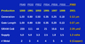
The table below shows the history of Intel's process scaling. Values were taken from various Intel documents including IDF presentations, ISSCC papers, and IEDM papers. Note that while a great deal of effort was put into ensuring the accuracy of the values, some numbers vary to a small degree between Intel's own documents and therefore discrepancies may exist. SRAM bitcell areas refer to a high-density 6T bitcell with the exception of the very first few processes where smaller cell designs were used. Additionally, the metal layer count is for the client dies (example consumer mobile & desktop); server models utilize considerably more layers. Finally, from the 45 nm node, Intel has switched to utilizing a high-κ material, therefore the oxide thickness shown refers to the equivalent oxide thickness instead.
Nomenclature[edit]
Intel has been using the same naming scheme for decades. All process technologies (including packaging technologies) begin with a 'P' followed by the wafer size and the process ID. Generally, the process ID is an auto-increment value with odd values generally reserved for SoC and I/O (low power) devices while the even values have been used for Intel premier line of high-performance processors.

Timeline[edit]
| Year | Process | Node | MLayers | Intel µarchs | Gate | Interconnects | Attributes | |||
|---|---|---|---|---|---|---|---|---|---|---|
| 1972 | PMOS I (4004, 8008) |
10 µm | 1 | 4004 | Gate Dielectric | SiO2 | ||||
| Lg | 10.0 µm | |||||||||
| 1974 | HMOS I (4040) |
8 µm | 1 | 4040 | Gate Dielectric | SiO2 | ||||
| Lg | 8.0 µm | |||||||||
| 1976 | HMOS II/III (8080) |
6 µm | 1 | 8080 | Gate Dielectric | SiO2 | ||||
| Lg | 6.0 µm | |||||||||
| 1977 | CHMOS I (8086, 8088) |
3 µm | 1 | 8085, 8086, 8088 |
Tox | 70 nm | Gate Dielectric | SiO2 | ||
| Vdd | 5 V | SRAM | 1120 µm² | |||||||
| Lg | 3.0 µm | |||||||||
| CPP | 7 µm | MMP | 11 µm | |||||||
| 1979 | CHMOS II (80186) |
2 µm | 1 | 80186 | Tox | 40 nm | Gate Dielectric | SiO2 | ||
| Vdd | 5 V | SRAM | 1740 µm² | |||||||
| Lg | 2.0 µm | |||||||||
| CPP | 5.6 µm | MMP | 8 µm | |||||||
| 1982 | P646 (CHMOS III) |
1.5 µm | 1 | 80286, 80386 |
Tox | 25 nm | Gate Dielectric | SiO2 | ||
| Vdd | 5 V | SRAM | 951.7 µm² | |||||||
| Lg | 1.5 µm | |||||||||
| CPP | 4.0 µm | MMP | 6.4 µm | |||||||
| 1987 | P648 | 1.0 µm | 2 | 80486 | Tox | Gate Dielectric | SiO2 | |||
| Vdd | 5 V | SRAM | 220 µm² | |||||||
| Lg | 1.0 µm | |||||||||
| CPP | MMP | |||||||||
| 1989 | P650 | 0.8 µm | 3 | 80486 | Tox | 15 nm | Gate Dielectric | SiO2 | ||
| Vdd | 4 V | SRAM | 111 µm² | |||||||
| Lg | 800 nm | |||||||||
| CPP | 1.7 µm | MMP | 2 µm | |||||||
| 1991 | P652 | 0.6 µm | 4 | 80486, P5 |
Tox | 8 nm | Gate Dielectric | SiO2 | ||
| Vdd | 3.3 V | SRAM | ||||||||
| Lg | 600 nm | |||||||||
| CPP | MMP | 1.4 µm | ||||||||
| 1993 | P852 | 0.5 µm | 4 | P5 | Tox | 8 nm | Gate Dielectric | SiO2 | ||
| Vdd | 3.3 V | SRAM | 44 µm² | |||||||
| Lg | 500 nm | |||||||||
| CPP | MMP | |||||||||
| 1995 | P854 | 0.35 µm | 4 | P6 | Tox | 6 nm | Gate Dielectric | SiO2 | ||
| Vdd | 2.5 V | SRAM | 20.5 µm² | |||||||
| Lg | 350 nm | |||||||||
| CPP | 920 nm | MMP | 880 nm | |||||||
| 1997 | P856 | 0.25 µm | 5 | P6 | Tox | 4.08 nm | Gate Dielectric | SiO2 | ||
| Vdd | 1.8 V | SRAM | 10.26 µm² | |||||||
| Lg | 200 nm | |||||||||
| CPP | 500 nm | MMP | 640 nm | |||||||
| 1998 | P856.5 | 0.25 µm | 5 | P6 | Tox | 4.08 nm | Gate Dielectric | SiO2 | ||
| Vdd | 1.8 V | SRAM | 9.26 µm² | |||||||
| Lg | 200 nm | |||||||||
| CPP | 475 nm | MMP | 608 nm | |||||||
| 1999 | P858 | 0.18 µm | 6 | NetBurst |  |
Tox | 2.0 nm | Gate Dielectric | SiO2 | |
| Vdd | 1.6 V | SRAM | 5.59 µm² | |||||||
| Lg | 130 nm | |||||||||
| CPP | 480 nm | MMP | 500 nm | |||||||
| 2001 | P860 | 0.13 µm | 6 | Pentium M |  |
 | Tox | 1.4 nm | Gate Dielectric | SiO2 |
| Vdd | 1.4 V | SRAM | 2.45 µm² | |||||||
| Lg | 70 nm | |||||||||
| CPP | 336 nm | MMP | 345 nm | |||||||
| 2003 | P1262 (CPU) P1263 (SoC, I/O) |
90 nm | 7 | Pentium M |  |
 | Tox | 1.2 nm | Gate Dielectric | SiO2 |
| Vdd | 1.2 V | SRAM | 1.00 µm² | |||||||
| Lg | 50 nm | |||||||||
| CPP | 260 nm | MMP | 220 nm | |||||||
| 2005 | P1264 (CPU) P1265 (SoC, I/O) |
65 nm | 8 | Core, Modified Pentium M |
 |
 | Tox | 1.2 nm | Gate Dielectric | SiO2 |
| Vdd | SRAM | 0.570 µm² | ||||||||
| Lg | 35 nm | |||||||||
| CPP | 220 nm | MMP | 210 nm | |||||||
| 2007 | P1266 (CPU) P1267 (SoC, I/O) |
45 nm | 9 | Penryn, Nehalem |
 |
 | Toxe | 1 nm | Gate Dielectric | High-κ |
| Vdd | SRAM | 0.346 µm² | ||||||||
| Lg | 25 nm | |||||||||
| CPP | 160 nm | MMP | 180 nm | |||||||
| 2009 | P1268 (CPU) P1269 (SoC, I/O) |
32 nm | 10 | Westmere, Sandy Bridge |
 |
 | Toxe | 1 nm | Gate Dielectric | High-κ |
| Vdd | 0.75 V | SRAM | 0.148 µm² | |||||||
| Lg | 30 nm | |||||||||
| CPP | 112.5 nm | MMP | 112.5 nm | |||||||
| 2011 | P1270 (CPU) P1271 (SoC, I/O) |
22 nm | 11 | Ivy Bridge, Haswell |
 |
 | Toxe | 0.9 nm | Gate Dielectric | High-κ |
| Vdd | 0.75 V | SRAM | 0.092 µm² | |||||||
| Lg | 26 nm | |||||||||
| CPP | 90 nm | MMP | 80 nm | |||||||
| Pfin | 60 nm | |||||||||
| Wfin | 8 nm | Hfin | 34 nm | |||||||
| 2014 | P1272 (CPU) P1273 (SoC, I/O) |
14 nm | 12 | Broadwell, Skylake, Kaby Lake, Coffee Lake, Cascade Lake, Comet Lake, Cooper Lake, Rocket Lake |
 |
 | Toxe | Gate Dielectric | High-κ | |
| Vdd | 0.70 V | SRAM | 0.0499 µm² | |||||||
| Lg | 20 nm | |||||||||
| CPP | 70 nm | MMP | 52 nm | |||||||
| Pfin | 42 nm | |||||||||
| Wfin | 8 nm | Hfin | 42-46 nm | |||||||
| 2019 | P1274 (CPU) P1275 (SoC, I/O) |
10 nm | 12-13 | Cannon Lake, Ice Lake, Lakefield, Tiger Lake |
Toxe | Gate Dielectric | High-κ | |||
| Vdd | 0.70 V | SRAM | 0.0312 µm² | |||||||
| Lg | 18 nm | |||||||||
| CPP | 54 nm | MMP | 36 nm | |||||||
| Pfin | 34 nm | |||||||||
| Wfin | 7 nm | Hfin | 44-55 nm | |||||||
| 2021 | P1276 (CPU) P1277 (SoC, I/O) |
7 nm | Intel 7 | Alder Lake, Raptor Lake, Sapphire Rapids, Emerald Rapids |
Toxe | Gate Dielectric | ||||
| Vdd | SRAM | |||||||||
| Lg | ||||||||||
| CPP | MMP | |||||||||
| Pfin | ||||||||||
| Wfin | Hfin | |||||||||
| 2023 | P1278 (CPU) P1279 (SoC, I/O) |
5 nm | Intel 4 nm 3 nm node |
Meteor Lake, Granite Rapids |
Toxe | Gate Dielectric | ||||
| Vdd | SRAM | |||||||||
| Lg | ||||||||||
| CPP | MMP | |||||||||
| Pfin | ||||||||||
| Wfin | Hfin | |||||||||
| 2024 | P1280 (CPU) P1281 (SoC, I/O) |
3 nm | TSMC N3B |
Lunar Lake, Arrow Lake |
Toxe | Gate Dielectric | ||||
| Vdd | SRAM | |||||||||
| Lg | ||||||||||
| CPP | MMP | |||||||||
| Pfin | ||||||||||
| Wfin | Hfin | |||||||||
| 2025 | P1282 (CPU) P1283 (SoC, I/O) |
2 nm | Intel 18A |
Panther Lake, Diamond Rapids |
Toxe | Gate Dielectric | ||||
| Vdd | SRAM | |||||||||
| Lg | ||||||||||
| CPP | MMP | |||||||||
| Pfin | ||||||||||
| Wfin | Hfin | |||||||||
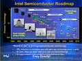
Intel Process Roadmap[edit]
| Intel Process Roadmap | ||||||||
|---|---|---|---|---|---|---|---|---|
| Process name | Intel 10 nm (SuperFin) |
Intel 7 | Intel 4 | Intel 3 | Intel 20A (TSMC N3B) |
Intel 18A | Intel 14A | Intel 14A-E |
| Transistor architecture |
FinFET | Optimized FinFET |
Optimized FinFET |
Optimized FinFET |
RibbonFET | Optimized RibbonFET |
TBD | TBD |
| Perf/Watt (over 10nm ESF) |
N/A | 10-15% | 20% | 18% | >20% ? | >25% ? | TBA | TBA |
| EUV | N/A | N/A | EUV | EUV | EUV | EUV | High-NA EUV | TBD |
| Products | Cannon Lake Tiger Lake Lakefield Gracemont Tremont |
Alder Lake Raptor Lake Bretnett Lake Emerald Rapids Sapphire Rapids |
Meteor Lake Xe-HP ? Xe-HPC ? Xe-HPG ? (6 nm) |
Granite Rapids Sierra Forest |
Lunar Lake Arrow Lake |
Panther Lake Diamond Rapids Clearwater Forest |
Wildcat Lake Nova Lake |
Razer Lake Titan Lake |
| Production | 2020 | 2021 | 2022 | 2023 | 2024 | 2025 | 2026 | 2027 ? |
Images[edit]
historical roadmap
Roadmap past 180 nm

Intel's fab roadmap from 2003


SRAM Scaling[edit]
For Intel, from 2 µm to 10 nm, SRAM 6T bit cells have had an average shrink of 0.496x in an attempt to maintain Moore's Law double density observation/requirement. Note that SRAM shrunk more significantly prior to the 65 nm process node. It should also be noted that logic typically scales better than the typical 6T SRAM cells, so raw logic density scaled more over time. Nonetheless, the size of the SRAM can be as much as three to four times the density of the typical logic cell.

Other processes[edit]
Semiconductor Process history by company:
- DEC
- Intel