(→Memory Hierarchy) |
(cache info) |
||
| Line 5: | Line 5: | ||
|designer=Zhaoxin | |designer=Zhaoxin | ||
|manufacturer=HLMC | |manufacturer=HLMC | ||
| + | |manufacturer 2=SMIC | ||
|introduction=December 28, 2017 | |introduction=December 28, 2017 | ||
|process=28 nm | |process=28 nm | ||
| Line 33: | Line 34: | ||
|extension 14=TXT | |extension 14=TXT | ||
|extension 15=RDSEED | |extension 15=RDSEED | ||
| + | |l1i=32 KiB | ||
| + | |l1i per=core | ||
| + | |l1i desc=8-way set associative | ||
| + | |l1d=32 KiB | ||
| + | |l1d per=core | ||
| + | |l1d desc=8-way set associative | ||
| + | |l2=4 MiB | ||
| + | |l2 per=cluster | ||
| + | |l2 desc=8-way set associative | ||
|predecessor=Zhangjiang | |predecessor=Zhangjiang | ||
|predecessor link=zhaoxin/microarchitectures/zhangjiang | |predecessor link=zhaoxin/microarchitectures/zhangjiang | ||
Revision as of 20:20, 27 May 2018
| Edit Values | |
| WuDaoKou µarch | |
| General Info | |
| Arch Type | CPU |
| Designer | Zhaoxin |
| Manufacturer | HLMC, SMIC |
| Introduction | December 28, 2017 |
| Process | 28 nm |
| Core Configs | 2, 4, 8 |
| Pipeline | |
| Type | Superscalar |
| OoOE | Yes |
| Speculative | Yes |
| Reg Renaming | Yes |
| Stages | 18 |
| Instructions | |
| ISA | x86-64 |
| Extensions | MMX, SSE, SSE2, SSE3, SSSE3, SSE4.1, SSE4.2, AVX, AVX2, AES, RDRND, BMI, BMI2, TXT, RDSEED |
| Cache | |
| L1I Cache | 32 KiB/core 8-way set associative |
| L1D Cache | 32 KiB/core 8-way set associative |
| L2 Cache | 4 MiB/cluster 8-way set associative |
| Succession | |
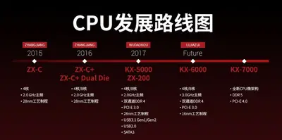
WuDaoKou is the successor to Zhangjiang, a 28 nm x86 microarchitecture designed by Zhaoxin for mainstream laptops, desktops, and servers.
Contents
Etymology
WuDaoKou is named after the Wudaokou Station of the Beijing Subway in China.
Brands
| Family | Series | Description |
|---|---|---|
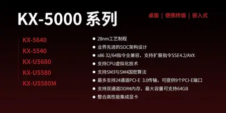
| KaiXian | KX (5000) | Desktop, Laptops |
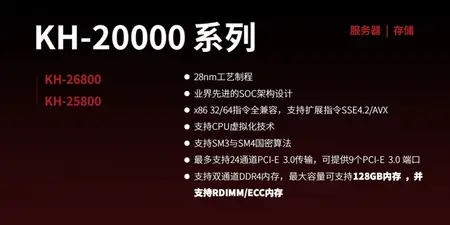
| KaisHeng | KH (20000) | Storage, Servers |
Release Dates
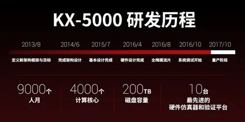
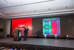
Development for WuDaoKou started in August 2013. The basic architecture design was completed by June 2014 with basic design done in July 2015. WuDaoKou hardware implementation was completed in April 2016 and taped out in August 2016. Final verification was done in October 2016 and mass production started in October 2017. The KX-5000 (formerly ZX-D) was announced at Semicon China 2017. The architecture and SKUs were officially unveiled at a conference on December 28, 2018.
WuDaoKou is said to be a result of 9,000 engineering months. Development data exceeded 200 TB with 4,000 cores being used for simulations with ten hardware emulators used for verification simulating a total of 150 billion instructions testing more than 300 different kinds of software, testing the CPU, GPU, memory controller, and bus.
Process Technology
WuDaoKou is manufactured on HLMC's 28 nm process.
Architecture
Key changes from Zhangjiang
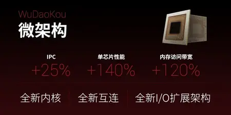
- 25% higher IPC
- 140% higher performance in multi-threaded workloads
- 8 cores per die (up from 4)
- SoC design
- New Uncore
- northbridge moved on-die
- PCIe 3.0 (from 2.0)
- DDR4 (From DDR3)
- New integrated graphics processor
- HD Audio Output/Codec
- DirectX 11.1
- Up to 3 displays
- DP (1.2a) / eDP (1.3) / HDMI (1.4b) / VGA
- New Uncore
- Core
- Improved OoOE algorithm
- Pipeline was reduced by 5 stages
- Execution engines were re-balanced
- Branch prediction unit was reworked and optimized
- FSB removed
- x4 PCIe 3.0 communication with southbridge chipset
- Chipset
- Gigabit Ethernet port (RGMII)
- USB 3.1 Gen2 (Type-C) ports
- SATA 3.0 ports
- Formal OS certification
- Windows Hardware Quality Labs (WHQL) certification
- Windows 7/10
- Windows Hardware Quality Labs (WHQL) certification
This list is incomplete; you can help by expanding it.
Block Diagram
Memory Hierarchy
- Cache
- L1D Cache
- 32 KiB, 8-way set associative
- Per core
- L1I Cache
- 32 KiB, 8-way set associative
- Per core
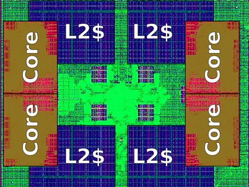
- L2 Cache
- 4 MiB, 8-way set associative
- Per quad-core cluster
- L1D Cache
- System DRAM
- 2 Channels
- DDR4, Up to 2400 MT/s
Overview
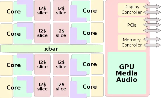
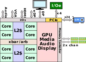
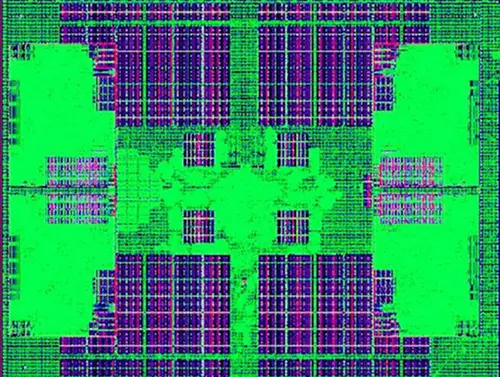
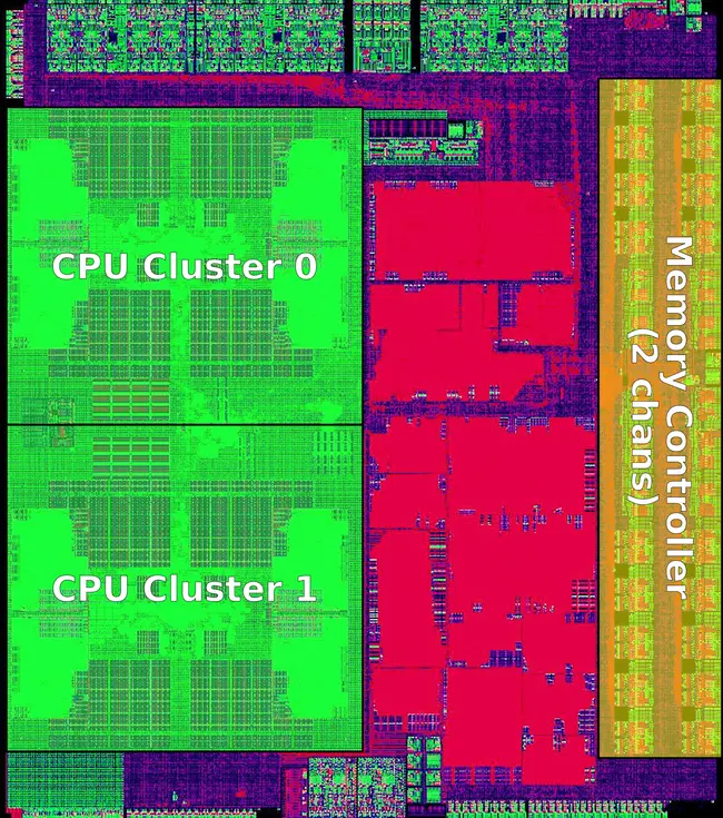
WuDaoKou is largely a brand new architecture designed by Zhaoxin. This is a departure from earlier microarchitectures such as ZhangJiang which were a lightly modified version of VIA Technologies (Centaur) architecture. WuDaoKou is a new and complete SoC design. Whereas prior processors had separate dies connected together over the legacy front-side bus, the new design is a single-die system-on-a-chip design that features 8 integrated x86 cores consisting of two clusters of four cores each connected over a new point-to-point crossbar, improving the internal bandwidth and latency considerably. The new chip also integrated the memory controller and the rest of the north-bridge on-die as well which further improved latency, bandwidth, and performance. The new chip also has an integrated graphics processor supporting 4K resolution and up to three screens via an array of display ports.
Overall, Zhaoxin has reported the new microarchitecture to have 25% improvement in IPC, 140% improvement in multi-core workloads, and 120% higher memory access bandwidth.
Uncore
WuDaoKou features a new point-to-point high-speed interconnect crossbar which replaces the front-side bus from prior architectures. The new crossbar reduces the latency and provides facilities for control flow and cache coherency. Going through the crossbar is also the newly integrated graphics processor as well the memory controller. The new memory controller now supports up to dual-channel DDR4 with data rates of up to 2400 MT/s (although current SKUs only seem to support up to 2133 MT/s). Zhaoxin has stated that this is the first domestic CPU to have a dual-channel DDR4 memory controller.
Core
Pipeline
WuDaoKou features an 18-stage pipeline with a 15 cycle misprediction penalty.
Graphics
The exact architecture of the GPU has not been disclosed but there is some evidence that suggest they may be using a S3 Graphics IP (originally owned by VIA Technologies as well but has since been purchased by HTC.) The GPU supports up to three displays using HDMI 1.4b, DisplayPort 1.2a, Embedded DisplayPort 1.3, and VGA. The GPU supports DirectX 11.1 and up to 4K resolution.
Sockets/Platform
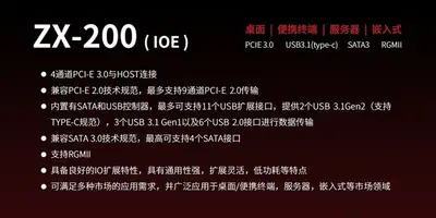
All parts use a HFCBGA 37.5×37.5 mm package and are effectively a system on a chip. However, for the most part, those parts get paired with a chipset which serves as an I/O extension chip. The chipset communicates with the microprocessor over standard PCIe 3.0 x4 lanes.
| Chipset | ||||||||||
|---|---|---|---|---|---|---|---|---|---|---|
| Chipset | TDP | PCIe | SATA | USB | Network | Process | Package | |||
| 2.0 | 3.0 | 3.0 | 2.0 | 3.1 Gen 1 | 3.1 Gen 2 | |||||
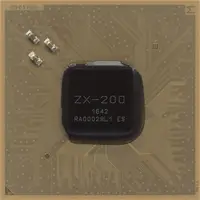
| ZX-200 | 6 W | 9 lanes | - | 4 | 6 | 3 | 2 | 10/100M/1 Gbps | 40 nm | FCBGA (21mm x 21mm) |
Die
Core module
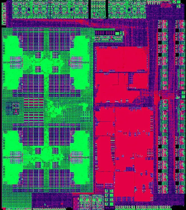
Octa-core die
- HLMC 28 nm process
- 187 mm² die size
- 2,100,000,000 transistors
All WuDaoKou Processors
| List of WuDaoKou-based Processors | |||||||
|---|---|---|---|---|---|---|---|
| Main processor | |||||||
| Model | Family | Launched | Cores | L2 | Frequency | Max Memory | ECC |
| KH-25800 | KaisHeng | 28 December 2017 | 8 | 8 MiB 8,192 KiB 8,388,608 B 0.00781 GiB | 1.8 GHz 1,800 MHz 1,800,000 kHz | 128 GiB 131,072 MiB 134,217,728 KiB 137,438,953,472 B 0.125 TiB | ✔ |
| KH-26800 | KaisHeng | 28 December 2017 | 8 | 8 MiB 8,192 KiB 8,388,608 B 0.00781 GiB | 2 GHz 2,000 MHz 2,000,000 kHz | 128 GiB 131,072 MiB 134,217,728 KiB 137,438,953,472 B 0.125 TiB | ✔ |
| KX-5540 | KaiXian | 28 December 2017 | 4 | 4 MiB 4,096 KiB 4,194,304 B 0.00391 GiB | 1.8 GHz 1,800 MHz 1,800,000 kHz | 64 GiB 65,536 MiB 67,108,864 KiB 68,719,476,736 B 0.0625 TiB | ✘ |
| KX-5640 | KaiXian | 28 December 2017 | 4 | 4 MiB 4,096 KiB 4,194,304 B 0.00391 GiB | 2 GHz 2,000 MHz 2,000,000 kHz | 64 GiB 65,536 MiB 67,108,864 KiB 68,719,476,736 B 0.0625 TiB | ✘ |
| KX-U5580 | KaiXian | 28 December 2017 | 8 | 8 MiB 8,192 KiB 8,388,608 B 0.00781 GiB | 1.8 GHz 1,800 MHz 1,800,000 kHz | 64 GiB 65,536 MiB 67,108,864 KiB 68,719,476,736 B 0.0625 TiB | ✘ |
| KX-U5580M | KaiXian | 28 December 2017 | 8 | 8 MiB 8,192 KiB 8,388,608 B 0.00781 GiB | 1.8 GHz 1,800 MHz 1,800,000 kHz | 64 GiB 65,536 MiB 67,108,864 KiB 68,719,476,736 B 0.0625 TiB | ✘ |
| KX-U5680 | KaiXian | 28 December 2017 | 8 | 8 MiB 8,192 KiB 8,388,608 B 0.00781 GiB | 2 GHz 2,000 MHz 2,000,000 kHz | 64 GiB 65,536 MiB 67,108,864 KiB 68,719,476,736 B 0.0625 TiB | ✘ |
| Count: 7 | |||||||
Documents
References
- Information was obtained directly from Zhaoxin
- Zhaoxin launches their highest-performance Chinese x86 chips
| codename | WuDaoKou + |
| core count | 2 +, 4 + and 8 + |
| designer | Zhaoxin + |
| first launched | December 28, 2017 + |
| full page name | zhaoxin/microarchitectures/wudaokou + |
| instance of | microarchitecture + |
| instruction set architecture | x86-64 + |
| manufacturer | HLMC + and SMIC + |
| microarchitecture type | CPU + |
| name | WuDaoKou + |
| pipeline stages | 18 + |
| process | 28 nm (0.028 μm, 2.8e-5 mm) + |
