| Edit Values | |
| TaiShan v110 µarch | |
| General Info | |
| Arch Type | CPU |
| Designer | HiSilicon |
| Manufacturer | TSMC |
| Introduction | 2019 |
| Process | 7 nm |
| Core Configs | 32, 48, 64 |
| Pipeline | |
| Type | Superscalar, Superpipeline |
| OoOE | Yes |
| Speculative | Yes |
| Reg Renaming | Yes |
| Decode | 4-way |
| Instructions | |
| ISA | ARMv8.2-A |
| Extensions | NEON |
| Cache | |
| L1I Cache | 64 KiB/core |
| L1D Cache | 64 KiB/core |
| L2 Cache | 512 KiB/core |
| L3 Cache | 1 MiB/core |
| Succession | |
TaiShan v110 is the successor to the TaiShan v100, a high-performance ARM server microarchitecture designed by HiSilicon for Huawei's own TaiShan servers.
Contents
Brands[edit]
TaiShan-based CPUs are branded as the Kunpeng 920 series.
Release Dates[edit]
Kunpeng 920 CPUs were officially launched in early 2019.
Architecture[edit]
Key changes from TaiShan v100[edit]
- TSMC 7 nm HPC process (from 16 nm)
- 2x core count (64, up from 32)
- Custom cores (from Cortex-A72)
- ASIMD
- double SP Vector throughput (2 inst/cycle, up from 1)
- ASIMD
- Custom cores (from Cortex-A72)
- Memory
- 2x memory channels (8, up from 4)
- I/O
- PCIe Gen 4 (from Gen 3)
This list is incomplete; you can help by expanding it.
Block Diagram[edit]
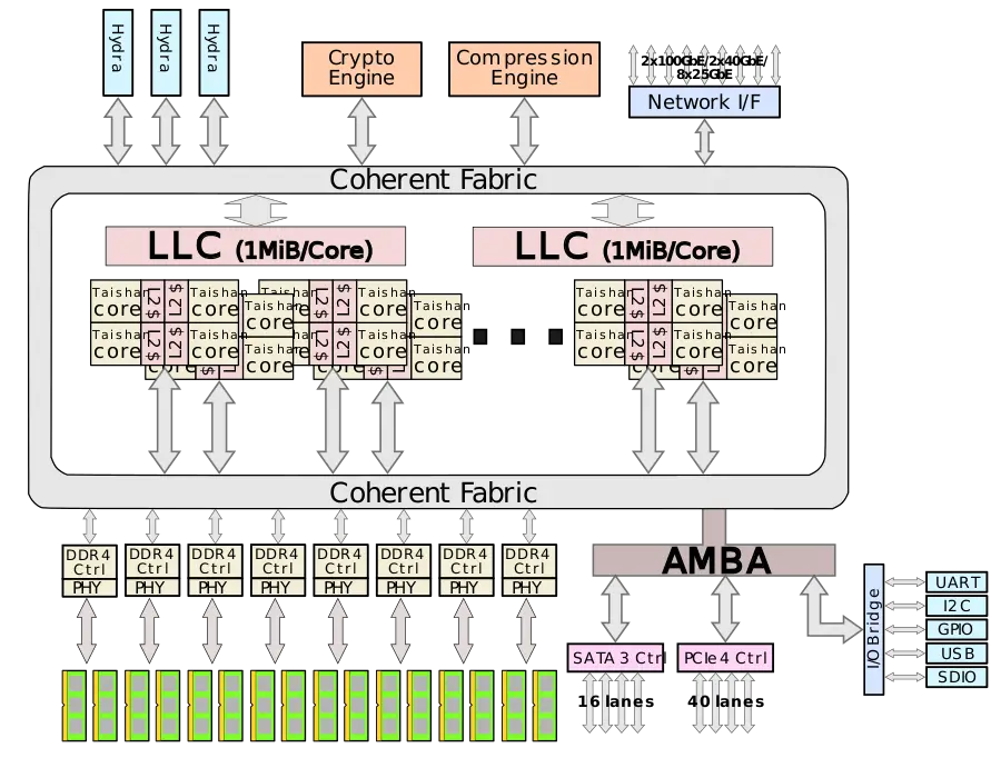
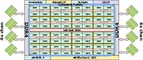
Entire Chip[edit]
Memory Hierarchy[edit]
- Cache
- L1I Cache
- 64 KiB/core, private
- 64-byte cache lines
- L1D Cache
- 64 KiB/core, private
- 64-byte cache lines
- L2 Cache
- 512 KiB/core, private
- L3 Cache
- 1 MiB/core
- Shared by all cores
- System DRAM
- 1 TiB Max Memory / socket
- 8 Channels
- DDR4, up to 2933 MT/s
- 1 DPC and 2 DPC support
- 8 B/cycle/channel (@ memory clock)
- ECC, SDDC, DDDC
- L1I Cache
Overview[edit]
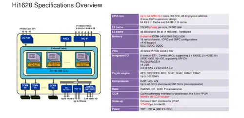
Though HiSilicon has a history of designing Arm processors. The TaiShan v110 core is HiSilicons' first custom homegrown high-performance ARM core and SoC design. The chip, which incorporates multiple compute dies and an I/O is a multi-chip package, is fabricated on TSMC's 7-nanometers HPC process and integrates up to 64 cores and up to 64 MiB of last level cache.
The SoC also incorporates a number of hardware accelerators. There is a crypto engine that supports AES, DES/3DES, MD5, SHA1, SHA2, HMAC, CMAC with throughputs of up to 100 Gbit/s. Additionally, there is also a compression engine supporting GZIP, LZS, LZ4 with compression throughputs of up to 40 Gbit/s and decompression of up to 100 Gbit/s.
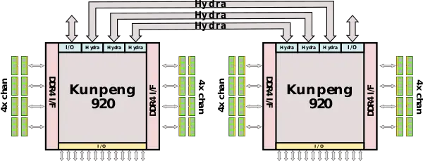
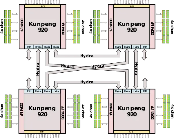
Marketed as the Kunpeng 920, this SoC supports up to 4-way multiprocessing support through HiSilicon's Hydra interface. In order to keep the cores fed, eight DDR4 memory channels are incorporated per socket. Additionally, designed to facilitate an easy accelerator platform, there are 40 PCIe Gen 4 lanes provided per socket with CCIX support, enabling cache coherency.
Core[edit]
Each core is a 4-way out-of-order superscalar that implements the ARMv8.2-A ISA. Huawei stated that the core supports almost all the ARMv8.4 features with a few exceptions, including dot product and the FP16 FML extension. It features private 64 KiB L1 instruction and data caches as well as 512 KiB of private L2. Though light on details, Huawei says that compared to Arm's Cortex cores, their core features an improved memory subsystem, a larger number of execution units, and a better branch predictor.
ASIMD[edit]
Each core features a single 128-bit NEON unit. It is capable of executing single double-precision FMA vector instruction per cycle or two single-precision vector instructions per cycle. Operating at 2 GHz, a 64-core chip will have a peak compute of 512 GigaFLOPS of double-precision floating point. It's worth noting that compared to the TaiShan v100, the throughput for single-precision vector has been doubled from 1 to 2 instructions per cycle.
MCP physical design[edit]
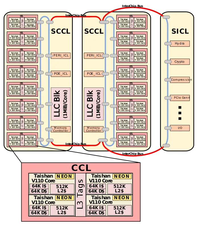
The SoC itself comprises 3 dies - two Super CPU Cluster (SCCL) compute dies and a Super IO Cluster (SICL). The SCCL compute dies contains 8 CPU Clusters (CCLs), memory controllers, and the L3 cache block. There are eight CCLs on each of the SICL dies for a total of 64 cores. The CCLs are TaiShan V110 quadplex along with the L3 cache tags partition. The Super IO Clusters include the various I/O peripherals including PCIe Gen 4, SAS, the network interface controllers, and the Hydra links.
Scalability[edit]
- See also: Hydra Interface
Each chip incorporates three Hydra interface ports. The Hydra interface facilitates the cache coherency between the dies on the chip. Every link supports 240 Gb/s (30 GB/s) of peak bandwidth for a total aggregated bandwidth of 720 Gb/s (90 GB/s) in a 2-way symmetric multiprocessing configuration.
With all three links, there is also support for 4-way SMP. In this configuration, one link from each socket is connected to another socket for an all-for-all connection.
Chipset[edit]
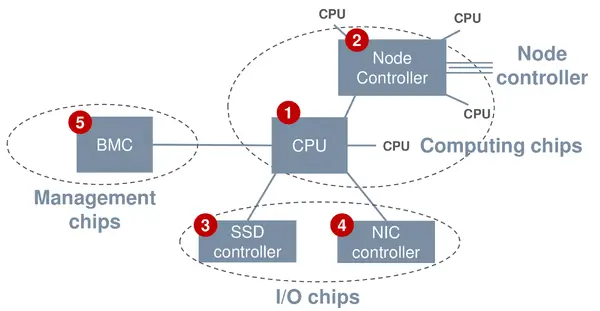
Along with the Hi1620 SoC, HiSilicon developed a number of integrated circuits as part of the chipset platform.
| Chip | Description |
|---|---|
| Hi1620 | CPU, Kunpeng 920 series Chip |
| Hi1503 | CPU interconnect chip, supports scaling-up to 32 sockets |
| Hi1812 | SSD storage controller, for read/write I/O acceleration |
| Hi1822 | Network controller chip, DC high-speed flexible interconnect |
| Hi1710 | BMC management chip + enhanced RAS features chip |
Die[edit]
- TSMC 7 nm HPC
- 20,000,000,000 transistors
- 3-4 dies
All TaiShan v110 Chips[edit]
| List of TaiShan v110-based Processors | ||||||
|---|---|---|---|---|---|---|
| Model | Launched | Cores | Arch | Frequency | L3 | TDP |
| 920-3226 | 26 April 2019 | 32 | TaiShan v110 | 2.6 GHz 2,600 MHz 2,600,000 kHz | 32 MiB 32,768 KiB 33,554,432 B 0.0313 GiB | 120 W 120,000 mW 0.161 hp 0.12 kW |
| 920-4826 | 26 April 2019 | 48 | TaiShan v110 | 2.6 GHz 2,600 MHz 2,600,000 kHz | 48 MiB 49,152 KiB 50,331,648 B 0.0469 GiB | 158 W 158,000 mW 0.212 hp 0.158 kW |
| 920-6426 | 7 January 2019 | 64 | TaiShan v110 | 2.6 GHz 2,600 MHz 2,600,000 kHz | 64 MiB 65,536 KiB 67,108,864 B 0.0625 GiB | 195 W 195,000 mW 0.261 hp 0.195 kW |
| Count: 3 | ||||||
Bibliography[edit]
- Huawei. Personal Communication. 2019
- Huawei Connect 2018. October 2018
- HiSilicon Event. January 7, 2019
- Huawei, Supercomputing 2018
| codename | TaiShan v110 + |
| core count | 32 +, 48 + and 64 + |
| designer | HiSilicon + |
| first launched | 2019 + |
| full page name | hisilicon/microarchitectures/taishan v110 + |
| instance of | microarchitecture + |
| instruction set architecture | ARMv8.2-A + |
| manufacturer | TSMC + |
| microarchitecture type | CPU + |
| name | TaiShan v110 + |
| process | 7 nm (0.007 μm, 7.0e-6 mm) + |
