Semiconductor & Computer Engineering
| Edit Values | |
| Skylake µarch | |
| General Info | |
| Arch Type | CPU |
| Designer | Intel |
| Manufacturer | Intel |
| Introduction | August 5, 2015 |
| Process | 14 nm |
| Core Configs | 2, 4, 6, 8, 10, 12, 14, 16, 18, 20, 22, 24, 26, 28 |
| Pipeline | |
| Type | Superscalar |
| OoOE | Yes |
| Speculative | Yes |
| Reg Renaming | Yes |
| Stages | 14-19 |
| Instructions | |
| ISA | x86-16, x86-32, x86-64 |
| Extensions | MOVBE, MMX, SSE, SSE2, SSE3, SSSE3, SSE4.1, SSE4.2, POPCNT, AVX, AVX2, AES, PCLMUL, FSGSBASE, RDRND, FMA3, F16C, BMI, BMI2, VT-x, VT-d, TXT, TSX, RDSEED, ADCX, PREFETCHW, CLFLUSHOPT, XSAVE, SGX, MPX, AVX-512 |
| Cache | |
| L1I Cache | 32 KiB/core 8-way set associative |
| L1D Cache | 32 KiB/core 8-way set associative |
| L2 Cache | 256 KiB/core 4-way set associative |
| L3 Cache | 2 MiB/core Up to 16-way set associative |
| Side Cache | 128 MiB/package on Iris Pro GPUs only |
| Cores | |
| Core Names | Skylake Y, Skylake U, Skylake H, Skylake S, Skylake DT, Skylake X, Skylake SP |
| Succession | |
Skylake (SKL) is Intel's successor to Broadwell, a 14 nm process microarchitecture for mainstream desktops, servers, and mobile devices. Skylake succeeded the short-lived Broadwell which experienced severe delays. Skylake is the "Architecture" phase as part of Intel's PAO model. The microarchitecture was developed by Intel's R&D center in Haifa, Israel.
For desktop and mobile, Skylake is branded as 6th Generation Intel Core i3, Core i5, Core i7, and Core i9 processors. For workstations it's branded as Xeon E3 v5 For scalable server class processors, Intel branded it as Xeon Bronze, Xeon Silver, Xeon Gold, and Xeon Platinum.
Contents
- 1 Codenames
- 2 Brands
- 3 Release Dates
- 4 Process Technology
- 5 Compatibility
- 6 Compiler support
- 7 Architecture
- 8 Overview (Client)
- 9 Overview (Server)
- 10 New Technologies
- 11 Power
- 12 Clock domains
- 13 New Integration
- 14 Graphics
- 15 Sockets/Platform
- 16 Die
- 17 All Skylake Chips
- 18 References
- 19 Documents
- 20 See also
Codenames
| Core | Abbrev | Target |
|---|---|---|
| Skylake Y | SKL-Y | 2-in-1s detachable, tablets, and computer sticks |
| Skylake U | SKL-U | Light notebooks, portable All-in-Ones (AiOs), Minis, and conference room |
| Skylake H | SKL-H | Ultimate mobile performance, mobile workstations |
| Skylake S | SKL-S | Desktop performance to value, AiOs, and minis |
| Skylake X | SKL-X | High-end desktops & enthusiasts market |
| Skylake DT | SKL-DT | Workstations & entry-level servers |
| Skylake SP | SKL-SP | Server Scalable Processors |
Brands

Intel released Skylake under 7 main brand families.
Additionally, Intel introduced a number of new server chip families with the introduction of Skylake SP.
| Logo | Family | General Description | Differentiating Features | ||||||
|---|---|---|---|---|---|---|---|---|---|
| Cores | HT | AVX | AVX2 | AVX-512 | TBT | ECC | |||
 |
Celeron | Entry-level Budget | dual | ✘ | ✘ | ✘ | ✘ | ✘ | ✘ |
| Entry-level Budget (Embedded) | ✘ | ✘ | ✘ | ✘ | ✘ | ✔ | |||
 |
Pentium | Budget (Mobile) | dual | ✔ | ✘ | ✘ | ✘ | ✘ | ✘ |
| Budget (Desktop) | ✘ | ✘ | ✘ | ✘ | ✘ | ✔ | |||
| |
Core i3 | Low-end Performance | dual | ✔ | ✔ | ✔ | ✘ | ✘ | ✘ |
| Low-end Performance (Desktop/Embedded) |
✔ | ✔ | ✔ | ✘ | ✘ | ✔ | |||
| |
Core i5 | Mid-range Performance | dual | ✔ | ✔ | ✔ | ✘ | ✔ | ✘ |
| quad | ✘ | ✔ | ✔ | ✘ | ✔ | ✘ | |||
| |
Core i7 | High-end Performance | dual | ✔ | ✔ | ✔ | ✘ | ✔ | ✘ |
| quad | ✔ | ✔ | ✔ | ✘ | ✔ | ✘ | |||
| Enthusiasts/High Performance (X) | 6 - 8 | ✔ | ✔ | ✔ | ✔ | ✔ | ✘ | ||
| |
Xeon E3 | Workstation/dense servers | quad | ✔/✘ | ✔ | ✔ | ✘ | ✔ | ✔ |
| |
Core i9 | Enthusiasts/High Performance | 10 - 18 | ✔ | ✔ | ✔ | ✔ | ✔ | ✘ |
| Logo | Family | General Description | Differentiating Features | ||||||
| Cores | HT | TBT | AVX-512 | AVX-512 Units | UPI links | Scalability | |||
.png) |
Xeon Bronze | Entry-level performance / Cost-sensitive |
6 - 8 | ✘ | ✘ | ✔ | 1 | 2 | Up to 2 |
.png) |
Xeon Silver | Mid-range performance / Efficient lower power |
4 - 12 | ✔ | ✔ | ✔ | 1 | 2 | Up to 2 |
.png) |
Xeon Gold 5000 | High performance | 4 - 14 | ✔ | ✔ | ✔ | 1 | 2 | Up to 4 |
| Xeon Gold 6000 | Higher performance | 6 - 22 | ✔ | ✔ | ✔ | 2 | 3 | Up to 4 | |
.png) |
Xeon Platinum | Highest performance / flexibility | 4 - 28 | ✔ | ✔ | ✔ | 2 | 3 | Up to 8 |
Release Dates
Skylake was first demonstrated at the 2014 Intel Developer Forum in San Francisco on September 9 with the goals of launching in the second half of 2015. Skylake-based Core X was introduced in May 2017 while Skylake SP was introduced in July 2017.
Process Technology
- Main article: Broadwell § Process Technology
Skylake uses the same 14 nm process used for the Broadwell microarchitecture for all mainstream consumer parts (Core, Celeron, et al). Unlike mainstream Skylake models, the enthusiasts (Skylake X) models are fabricated on Intel's enhanced 14+ nm process which is used by Kaby Lake (see Kaby Lake § Process Technology for more info).
Compatibility
| Vendor | OS | Version | Notes |
|---|---|---|---|
| Microsoft | Windows | Windows Vista | No Support |
| Windows 7 | Support ends July 2017 | ||
| Windows 8.1 | |||
| Windows 10 | Support | ||
| Linux | Linux | Kernel 3.19 | Initial Support (MPX support) |
| Chromium | Chromium | Support | |
| Wind River | VxWorks | VxWorks 5.5? | Support |
Compiler support
| Compiler | Arch-Specific | Arch-Favorable |
|---|---|---|
| ICC | -march=skylake |
-mtune=skylake
|
| GCC | -march=skylake |
-mtune=skylake
|
| LLVM | -march=skylake |
-mtune=skylake
|
| Visual Studio | /arch:AVX2 |
/tune:skylake
|
CPUID
| Core | Extended Family |
Family | Extended Model |
Model |
|---|---|---|---|---|
| Y/U | 0 | 0x6 | 0x4 | 0xE |
| Family 6 Model 78 | ||||
| DT/H/S/X | 0 | 0x6 | 0x5 | 0xE |
| Family 6 Model 94 | ||||
| SP | 0 | 0x6 | 0x5 | 0x5 |
| Family 6 Model 85 | ||||
Architecture
Overall Skylake builds upon Intel's previous microarchitecture, Broadwell, but includes a wider and more beefed up front end, more optimized execution engine, and numerous other enhancements. Intel designed Skylake to encompass a wide range of devices and applications with a large emphasis on mobile with models ranging from as low as 4.5 W to as high as 100 W.
Key changes from Broadwell

- 8x performance/watt over Nehalem (Up from 3.5x in Haswell)
- Mainstream chipset
- Lynx Point → Sunrise Point
- Bus/Interface to Chipset
- DMI 3.0 (from 2.0)
- Skylake S and Skylake H cores, connected by 4-lane DMI 3.0
- Skylake Y and Skylake U cores have chipset in the same package (simplified OPIO)
- Increase in transfer rate from 5.0 GT/s to 8.0 GT/s (~3.93GB/s up from 2GB/s) per lane
- Limits motherboard trace design to 7 inches max from (down from 8) from the CPU to chipset
- DMI 3.0 (from 2.0)
- PCIe & DMI upgraded to Gen3
- More I/O (configurable as PCIe/SATA/USB3)
- Lower-power I/O (eMMC, UFS, SDXC)
- CSI-2 for the integrated IPU (mobile SKUs)
- Intel Sensor Solution Hub integration
- System Agent
- New Image Processing Unit (IPU)
- Incorporates an image signal processor (ISP)
- Mobile client models only
- Can now have its own variable voltage and frequency
- New Image Processing Unit (IPU)
- Core
- Front End
- Larger legacy pipeline delivery (5 µOPs, up from 4)
- Another simple decoder has been added.
- Allocation Queue (IDQ)
- Larger delivery (6 µOPs, up from 4)
- 2.28x larger buffer (64/thread, up from 56)
- Partitioned for each active threads (from unified)
- Improved branch prediction unit
- reduced penalty for wrong direct jump target
- No specifics were disclosed
- µOP Cache
- instruction window is now 64 Bytes (from 32)
- 1.5x bandwidth (6 µOPs/cycle, up from 4)
- Larger legacy pipeline delivery (5 µOPs, up from 4)
- Execution Engine
- Larger re-order buffer (224 entries, up from 192)
- Larger scheduler (97 entries, up from 64)
- Larger Integer Register File (180 entries, up from 168)
- Larger Retire (4 µOPs/cycle/thread, up from 4 µOPs/cycle/core)?
- Memory Subsystem
- Larger store buffer (56 entries, up from 42)
- L2$ was changed from 8-way to 4-way set associative
- Page split load penalty reduced 20-fold
- Larger Write-back buffer
- Larger Line Fill Buffer?
- Front End
- Memory
- Support for faster DDR-2400 memory
- L3$ re-gained 512 KiB/core (See §eDRAM architectural changes for the reason)
- A new coherent cache fabric implementation
- doubles the throughput of the last level cache (LLC, L3$ in this case) miss handling
- 50% improvement in bandwidth/watt
- new eDRAM cache architecture for higher bandwidth
- TLBs
- ITLB
- 4 KiB page translations was changed from 4-way to 8-way associative
- STLB
- 4 KiB + 2 MiB page translations was changed from 6-way to 12-way associative
- ITLB
- Electrical
- The fully integrated voltage regulator (FIVR) is moved back to the motherboard
- Originally intended to be a cost-cutting measure by moving the FIVR on-die as well as making it more efficient, the move resulted in unintentionally making the FIVR the limiting factor when it came to overclocking.
- DMI/PEG are now on a discrete clock domain with BCLK sitting on its own domain with full-range granularity (1 MHz intervals)
- The fully integrated voltage regulator (FIVR) is moved back to the motherboard
- Testability
- New support for Direct Connect Interface (DCI), a new debugging transport protocol designed to allow debugging of closed cases (e.g. laptops, embedded) by accessing things such as JTAG through any USB 3 port.
- Gen 9 GPUs
- Improved underlying implementation of the memory QoS for higher resolution displays and the integrated image signal processor (ISP)
- Allow for higher concurrent bandwidth
- Skylake retires VGA support, multi-monitor support for up to 3 displays via HDMI 1.4, DP 1.2, and eDP 1.3 interfaces.
- Direct X 12, OpenCL 2.0, OpenGL 4.4
- Up to 24 EUs GT2 (same as Haswell); 48 EUs for GT3, and up to 72 EUs on Iris Pro Graphics
- 1,152 GFLOPS @ 1 GHz
- Improved underlying implementation of the memory QoS for higher resolution displays and the integrated image signal processor (ISP)
Server

Unlike client models, Skylake servers and HEDT models will still incorporate the fully integrated voltage regulator (FIVR) on-die. Those chips also have an entirely new multi-core architecture along with a new mesh topology interconnect network (from ring topology).
- Improved "14 nm+" process (see Kaby Lake § Process Technology)
- Omni-Path Architecture (OPA)
- Mesh architecture
- Sub-NUMA Clustering (SNC) support (replaces the Cluster-on-Die (COD) implementation)
- Core
- Front-end
- LSD is disabled
- Back-end
- Port 4 now performs 512b stores (from 256b)
- Port 0 & Port 1 can now be fused to perform AVX-512
- Port 5 now can do full 512b operations (not on all models)
- Memory Subsystem
- Store is now 64B/cycle (from 32B/cycle)
- Load is now 2x64B/cycle (from 2x32B/cycle)
- Front-end
- Memory
- L2$
- Increased to 1 MiB/core (from 250 KiB/core)
- L3$
- Was made non-inclusive (from inclusive)
- Reduced to 1.375 MiB/core (from 2.5 MiB/core)
- DRAM
- hex-channel DDR4-2666 (from quad-channel)
- L2$
CPU changes
- Most ALU operations have 4 op/cycle 1 for 8 and 32-bit registers. 64-bit ops are still limited to 3 op/cycle. (16-bit throughput varies per op, can be 4, 3.5 or 2 op/cycle).
- MOVSX and MOVZX have 4 op/cycle throughput for 16->32 and 32->64 forms, in addition to Haswell's 8->32, 8->64 and 16->64 bit forms.
- ADC and SBB have throughput of 1 op/cycle, same as Haswell.
- Vector moves have throughput of 4 op/cycle (move elimination).
- Not only zeroing vector vpXORxx and vpSUBxx ops, but also vPCMPxxx on the same register, have throughput of 4 op/cycle.
- Vector ALU ops are often "standardized" to latency of 4. for example, vADDPS and vMULPS used to have L of 3 and 5, now both are 4.
- Fused multiply-add ops have latency of 4 and throughput of 0.5 op/cycle.
- Throughput of vADDps, vSUBps, vCMPps, vMAXps, their scalar and double analogs is increased to 2 op/cycle.
- Throughput of vPSLxx and vPSRxx with immediate (i.e. fixed vector shifts) is increased to 2 op/cycle.
- Throughput of vANDps, vANDNps, vORps, vXORps, their scalar and double analogs, vPADDx, vPSUBx is increased to 3 op/cycle.
- vDIVPD, vSQRTPD have approximately twice as good throughput: from 8 to 4 and from 28 to 12 cycles/op.
- Throughput of some MMX ALU ops (such as PAND mm1, mm2) is decreased to 2 or 1 op/cycle (users are expected to use wider SSE/AVX registers instead).
New instructions
Skylake introduced a number of new instructions:
- Client:
-
SGX1- Software Guard Extensions, Version 1 -
MPX-Memory Protection Extensions -
XSAVEC- Save processor extended states with compaction to memory -
XSAVES- Save processor supervisor-mode extended states to memory. -
CLFLUSHOPT- Flush & Invalidates memory operand and its associated cache line (All L1/L2/L3 etc..)
-
- Server
Block Diagram
Client SoC
Entire SoC Overview (dual)
.svg)
Entire SoC Overview (quad)

Individual Core

Gen9
See Gen9#Gen9.
Server MPUs
Server Chip
Note that the LCC die is identical without the two bottom rows. The XCC (28-core) die has one additional row and two additional columns of cores. Otherwise the die is identical.

- CHA - Caching and Home Agent
- SF - Snooping Filter
Individual Core

Memory Hierarchy
Client
Other than a few organizational changes (e.g. L2$ went from 8-way to 4-way set associative), the overall memory structure is identical to Broadwell/Haswell.
- Cache
- L0 µOP cache:
- 1,536 µOPs, 8-way set associative
- 32 sets, 6-µOP line size
- statically divided between threads, per core, inclusive with L1I
- 1,536 µOPs, 8-way set associative
- L1I Cache:
- 32 KiB, 8-way set associative
- 64 sets, 64 B line size
- shared by the two threads, per core
- 32 KiB, 8-way set associative
- L1D Cache:
- 32 KiB, 8-way set associative
- 64 sets, 64 B line size
- shared by the two threads, per core
- 4 cycles for fastest load-to-use (simple pointer accesses)
- 5 cycles for complex addresses
- 64 B/cycle load bandwidth
- 32 B/cycle store bandwidth
- Write-back policy
- L2 Cache:
- Unified, 256 KiB, 4-way set associative
- 1024 sets, 64 B line size
- Non-inclusive
- 12 cycles for fastest load-to-use
- 64 B/cycle bandwidth to L1$
- Write-back policy
- L3 Cache/LLC:
- Up to 2 MiB Per core, shared across all cores
- Up to 16-way set associative
- Inclusive
- 64 B line size
- Write-back policy
- Per each core:
- Read: 32 B/cycle (@ ring clock)
- Write: 32 B/cycle (@ ring clock)
- 42 cycles for fastest load-to-use
- Side Cache:
- System DRAM:
- 2 Channels
- 8 B/cycle/channel (@ memory clock)
- 42 cycles + 51 ns latency
- L0 µOP cache:
Skylake TLB consists of dedicated L1 TLB for instruction cache (ITLB) and another one for data cache (DTLB). Additionally there is a unified L2 TLB (STLB).
- TLBs:
- ITLB
- 4 KiB page translations:
- 128 entries; 8-way set associative
- dynamic partitioning
- 2 MiB / 4 MiB page translations:
- 8 entries per thread; fully associative
- Duplicated for each thread
- 4 KiB page translations:
- DTLB
- 4 KiB page translations:
- 64 entries; 4-way set associative
- fixed partition
- 2 MiB / 4 MiB page translations:
- 32 entries; 4-way set associative
- fixed partition
- 1G page translations:
- 4 entries; fully associative
- fixed partition
- 4 KiB page translations:
- STLB
- 4 KiB + 2 MiB page translations:
- 1536 entries; 12-way set associative
- fixed partition
- 1 GiB page translations:
- 16 entries; 4-way set associative
- fixed partition
- 4 KiB + 2 MiB page translations:
- ITLB
Server

The memory hierarchy for Skylake's server and HEDT processors has been rebalanced. Note that the L3 is now non-inclusive and some of the SRAM from the L3 cache was moved into the private L2 cache.
- Cache
- L2 Cache:
- Unified, 1 MiB, 16-way set associative
- 64 B line size
- Non-inclusive
- 64 B/cycle bandwidth to L1$
- Write-back policy
- 14 cycles latency
- L3 Cache:
- 1.375 MiB/s, shared across all cores
- Note that some models have non-default cache sizes which are larger due to some disabled cores
- 64 B line size
- 11-way set associative
- Non-Inclusive
- Write-back policy
- 50-70 cycles latency
- 1.375 MiB/s, shared across all cores
- L2 Cache:
Overview (Client)
- Main article: Client Architecture
Skylake inherits much of the Core design philosophy which was enhanced significantly over the past number of architectures. Skylake, like its predecessor Broadwell, is also a dual-threaded and complex out-of-order pipeline. Skylake which builds on Broadwell incorporates large number of enhancements that has improved performance and efficiency in order to cover a large spectrum of devices from ultra-low power to high-performance computing. Additionally, a large number of improvements were done to the integrated graphics and multimedia capabilities as well as a new set of security technologies were introduced.
Design goals & new goals

Skylake tries to address 4 major design goals: Scalability, Performance, Power, and Media & Graphics. Skylake started out as a "traditional client product" when initial design goals and development started back in 2010. At that time, Skylake was expected to cover products ranging from thin-and-lights all the way up to desktops. This translated to roughly 3x TDP scale and 2x form factor between the smallest and biggest models. With the introduction of Ultralight, Skylake design goals were extended to a new class of smaller form factors (down to 15 W). Skylake design goals were later further extended to more mobility segments and even smaller form factors. The final end result is a microarchitecture that now spans 20-fold TDP scale (from 3.5 W all the way to 80 W+) and up to 4-fold form factor between the lowest power model and the highest performance model. Intel claims that Skylake also succeeded in reducing power by 40-60% during important workloads such as video, graphics, and idle power which especially affect models where battery life is absolutely critical.
It's interesting to note that Skylake's end result managed to overlap and to some degree exceed Intel's own ultra-low power (ULP) series of microarchitectures (i.e. Silvermont and Goldmont).
Product Development Vectors:
- Form factor reduction - Emphasis was placed on reduction of form factor which includes both actual die size and package size.
- Platform minimization - Effort was spent on reducing the overall platform size include reduction of system board size, components, and power.
- Better life scenario power reduction - (mobile segment) The reduction of power during critical workloads such as video playback, video conferencing, and various other multimedia applications where the CPU itself is mostly idle.
- IA performance - Improvements to both power and performance of the CPU core
- IGP performance - Improvement to both power and performance of the GPU
- New Security technology - Better protection against hardware and software attacks
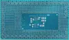
SoC design
.png)
The Skylake system on a chip consists of a five major components: CPU core, LLC, Ring interconnect, System agent, and the integrated graphics. The image shown on the right, presented by Intel at the Intel Developer Forum in 2015, represents a hypothetical model incorporating all available features Skylake has to offer (i.e. superset of features). Skylake features an improved core (see § Pipeline) with higher performance per watt and higher performance per clock. The number of cores depends on the model, but mainstream mobile models are typically dual-core while mainstream desktop models are typically quad-core with dual-core desktop models still offered for value models (e.g. Celeron). Accompanying the cores is the LCC (last level cache or L3$ as seen from the CPU perspective). On mainstream parts the LLC consists of 2 MiB for each core with lower amounts for value models. Connecting the cores together is the ring interconnect. The ring extends to the GPU and the system agent as well. Intel further optimized the ring in Skylake for low-power and higher bandwidth.
Accompanying the cores is the Gen9 integrated graphics unit which comes in a number of different tiers ranging from just 12 execution units (used in the ultra-low power models) all the way the GT4 (Gen9 § Pipeline) with 72 execution units boasting a peak performance of up to 2,534.4 GFLOPS (HF) / 1,267.2 GFLOPS (SP) on the highest-end workstation model. The two highest-tier models are also accompanied by dedicated eDRAM ranging from 64 GiB to 120 GiB in capacity. The eDRAM is packaged along with the SoC in the same package.
On the other side is the System Agent (SA) which houses the various functionality that's not directly related to the cores or graphics. Skylake features an upgraded integrated memory controller (IMC) with most mainstream models supporting faster memory and dual-channel DDR4. The SA in Skylake also includes the Display Controller which now supports higher resolution displays with up to three displays for all mainstream models.
The SA also incorporates up to 20 lanes of PCIe with lesser amounts depending on the model. Of the 20 lanes, x16 PCIe lanes are offered for an external dedicated graphics hookup with the other four lanes reserved for communication with the southbridge chipset over Intel's new proprietary DMI 3.0 bus. The upgrade from DMI 2.0 (used in previous architectures) to 3.0 increased the bandwidth by 60% (8.0 GT/s from 5). For some models where form factor is exceptionally critical, such as those used for ultralight device, the chipset is packaged along with the SoC utilizing an on-package-interconnect (OPI) instead.
The last component of the System Agent and an entirely new addition in Skylake is the Image Processing Unit (IPU) which incorporates an image signal processor (ISP) on-die. The IPU is only available on mobile models and was added in order to improve and streamline (i.e. form factor and consistent set of features and quality) the implementation and performance of tablets and 2-in-1s. Previously this would require the assistance of an external component and the implementations varied by designer.
Overview (Server)
- Main article: Server Architecture
Skylake-based servers have been entirely re-architected to meet the need for increased scalabiltiy and performance all while meeting power requirements. A superset model is shown on the right. Skylake-based servers are the first mainstream servers to make use of Intel's new mesh interconnect architecture, an architecture that was previously explored, experimented with, and enhanced with Intel's Phi many-core processors. Those processors are offered from 4 cores up to 28 cores with 8 to 56 threads. With Skylake, Intel now has a separate core architecture for those chips which incorporate a plethora of new technologies and features including support for the new AVX-512 instruction set extension.
All models incorporate 6 channels of DDR4 supporting up to 12 DIMMS for a total of 768 GiB (with extended models support 1.5 TiB). For I/O all models incorporate 48x (3x16) lanes of PCIe 3.0. There is an additional x4 lanes PCIe 3.0 reserved exclusively for DMI for the the Lewisburg chipset. For a selected number of models (specifically those with F suffix) have an Omni-Path Host Fabric Interface (HFI) on-package (see Integrated Omni-Path).
Skylake processors are designed for scalability, supporting 2-way, 4-way, and 8-way multiprocessing through Intel's new Ultra Path Interconnect (UPI) interconnect links, with two to three links being offered (see § Scalability). High-end models have node controller support allowing higher way (e.g., 32-way multiprocessing).
New Technologies
Client
Software Guard Extension (SGX)
- Main article: Intel's Software Guard Extension
Software Guard Extension (SGX) is a new inter-software guard x86 extension that allows software in user-level mode to create isolated secure environments called "enclaves" for storing data or code. Data and code stored in enclaves are protected from external processes including code executing with higher privileges including the operating system or a hypervisor (including all forms of debugging).
Memory Protection Extension (MPX)
- Main article: Intel's Memory Protection Extension
Memory Protection Extension (MPX) is a new x86 extension that offers a hardware-level bound checking implementation. This extension allows an application to define memory boundaries for allocated memory areas. The processors can then check all proceeding memory accesses against those boundaries to ensure accesses are not out of bound. A program accessing a boundary-marked buffer out of buffer will generate an exception.
Server
In addition to the client technologies, servers have a number of new technologies as well:
Key Protection Technology (KPT)
Key Protection Technology (KPT) is designed to help secure sensitive private keys in hardware at runtime. KPT augments QuickAssist Technology (QAT) hardware crypto accelerators with run-time storage of private keys using Intel's existing Platform Trust Technology (PTT), thereby allowing high throughput hardware security acceleration. The QAT accelerators are all integrated onto Intel's new Lewisburg chipset along with the Converged Security Manageability Engine (CSME) which implements Intel's PTT. The CSME is linked through a private hardware link that is invisible to x86 software and simple hardware probes.
Memory Protection Keys for Userspace (PKU)
Memory Protection Keys for Userspace (PKU also PKEYs) is an extension that provides a mechanism for enforcing page-based protections - all without requiring modification of the page tables when an application changes protection domains. PKU introduces 16 keys by re-purposing the 4 ignored bits from the page table entry.
Mode-Based Execute (MBE) Control
Mode-Based Execute (MBE) is an enhancement to the Extended Page Tables (EPT) that provides finer level of control of execute permissions. With MBE the previous Execute Enable (X) bit is turned into Excuse Userspace page (XU) and Execute Supervisor page (XS). The processor selects the mode based on the guest page permission. With proper software support, hypervisors can take advantage of this as well to ensure integrity of kernel-level code.
Power
"Speed Shift" (new power management)
Ever since the introduction of the modern power management unit on a microprocessor, it was effectively the role of the operating system to determine the desired operating frequency and voltage (i.e. a p-state) for the current workload. When the CPU utilization peaked, it was the role of the operating system to bump up the frequency to help cope with it. The issue has always been the limitation of the operating system. One such major limitation is the granularity of the operating system response time - usually in the 10s of milliseconds (anything lower than that would likely be too intensive and would not yield better result). A second major issue is that the operating system doesn't have an instantaneous observation of the microarchitectural behavior of the workload.
Intel introduced Speed Shift with Skylake, a new methodology for quickly alternating core frequencies in response to power loads. Intel introduced a new unit called Package Control Unit (PCU) which is effectively a full fledged microcontroller (containing power management logic and firmware) that collects and tracks many internal SoC statistics as well as external power telemetry (e.g. Psys and iMon). PCU is also capable of interfacing with the OS, BIOS, and DPTF. Speed Shift improves the performance of frequency shifting by off-loading the control from the operating system to the PCU.
Speed Shift effectively eliminates the need for the OS to manages the P-states - though it does have the final say (unless special exceptions occur such as thermal throttling). Intel calls this "autonomous P-state", allowing Speed Shift to kick in in a matter of just ~1 millisecond (whereas the operating system-based p-states control can be as slow as 30 ms). Speed Shift effectively reduces hitting peak frequency in around ~30 ms from over 100 ms (OS-based implementation as before). While Speed Shift is capable of full range shift by default, the operating system can set the minimum QoS, maximum frequency and power/performance hints when desired. The final result should be higher performance and specially higher responsiveness at power constrained form factors.
SpeedStep Technology Expansion
- Main article: SpeedStep Technology
Prior to Skylake, SpeedStep had three major domains: Cores, Integrated Graphics, and Coherent Fabric. With Skylake, SpeedStep has been extended to a number of new domains, including the System Agent, Memory, and the eDRAM I/O. Depending on the bandwidth consumption, SpeedStep can now save energy by reducing frequency on the new domains.
Information from the new domains, including additional thermal skin temperature control information is now supplied to OEMs.
Power of System (Psys)
Psys (Power of System) is a way for the PCU to monitor the performance and the total platform power provided to the chip. The chip uses a number of autonomous algorithms (one for "Low Range" and one for "High Range"). The Low Range algorithm frequency is lowered to conserve energy. Algorithm is capable of overriding the low P state - a state calculated ever millisecond based on the active workload and system characteristics. The High Range algorithm deals with elevating frequency for the benefit of increase performance (at the cost of increase energy/inefficiency). The exact ratio of ΔPower/ΔPerformance ≤ αPreference can be finely controlled via the OS and user preferences.
Other Power Optimization
Skylake includes a number of additional power optimization changes:
- AVX2 is now power gated - prior to Skylake, AVX2 was not power gated which meant it was susceptible to leakage. Starting with Skylake, those instruction are full power gated and turn off when not used.
- Many older/legacy underused resources have been downscaled.
- Various scenario-based power optimizations were done, including:
- Idle power is reduced further
- C1 state power reduction (improved dynamic capacitance Cdyn)
- For specific tasks such as streaming, Skylake is capable of powering down certain components of the GPU maintaining power on to the critical components needed for that purpose.
Overall Skylake enjoys better performance/Watt per core for 8x performance/watt over Nehalem.
AVX2 Power Gating
In Skylake, AVX2 has been entirely power-gated. The motive for this change is derived from the fact that applications either make heavy use of AVX2 instructions or don't use it at all. Most programs seldomly use AVX2 for only a small number of instructions. This gave Intel the ability to completely power gate it when the core execute code that does not make use of those instructions. Skylake requires a warm-up time before instructions can execute at full rate (in the order of a couple of 10,000s of cycles depending on frequency). Executing a dummy AVX2 instruction some time prior to heavy AVX2 workloads to prepare the CPU can avoid this.
Clock domains
Skylake is divided into a number of clock domains, each controlling the clock frequency of their respective unit in the processor. All clock domains are some multiple of the [virtual] bus clock (BCLK).
- BCLK - Bus/Base Clock - The system bus interface frequency (once upon a time referred to the actual FSB speed, it now serves as only a base clock reference for all other clock domains). The base clock is 100 MHz.
- Core Clock - The frequency at which the core and the L1/L2 caches operate at. (Frequency depends on the model and is represented as a multiple of BCLK).
- Ring Clock - The frequency at which the ring interconnect and LLC operate at. Data from/to the individual cores are read/written into the L3 at a rate of 32B/cycle operating at Ring Clock frequency.
- IGP Clock - The frequency at which the integrated graphics (Gen9 GPU) operates at. Data from/to the GPU are read/written into the LLC at a rate of 64B/cycle operating at this frequency as well.
- eDRAM Clock - The frequency at which the embedded DRAM operates at (only available for certain models). Data is read/written from/to the LLC at a rate of 32B/cycle operating at this frequency as well.
- MemClk - Memory Clock - The frequency at which the system DRAM operates at. DRAM data is transfered at a rate of 8B/cycle operating at MemClk frequency.

Overclocking
- See also: Intel's XMP

Skylake has improved overclocking capabilities greatly. Overclocking is generally done on unlocked parts such as the Core i7-6700K, Core i5-6600K, and the mobile Core i7-6820HK processor. Unlocked processors should be paired with a chipset such as the Z170 which offers the most overclocking capabilities such as unlocked BCLK, unlocked core ratio, unlocked memory ratio, unlocked GPU ratio, and voltage controls.
Skylake increased both the overclocking range and ratio granularity, allowing for much more finer overclocking.
| Core i7-3770K | Core i7-4790K | Core i7-6700K | |
|---|---|---|---|
| Core Ratios Override | Up to x63 | Up to x80 | Up to x83 |
| Real-time Core Ratio | ✔ | ✔ | ✔ |
| BCLK Overclocking | Limited | 100/125/167 MHz | 100+ in 1 MHz increments |
| MSR Voltage Control | SVID Extra Voltage | FIVR SVID Extra Voltage, Voltage Override, Interpolative | SVID Extra Voltage, Voltage Override, Interpolative |
| GPU Overclocking | All Chipsets | All Chipsets | All Chipsets |
| DDR Ratio/Frequency Override and MRC | Up to 2667 MT/s | Up to 2667 MT/s | Up to 4133 MT/s |
| DDR Granularity Steps | 200/266 MHz | 200/266 MHz | 100/133 MHz |
Note that core ratio has been increased to a [theoretical] x83 multiplier and the coarse-grain ratio was dropped from Skylake allowing a BCLK ratio to have granularity of 1 MHz increments with BCLK frequency of over 200 readily achievable. The FIVER was removed and the voltage control was given back to the motherboard manufacturers; i.e., voltage supplies can be entirely motherboard-controlled. Skylake also bumped the DDR ratio up to 4133 MT/s.

In the diagram on the left (xC) refers to the Core Frequency and is represented as a multiple of BCLK (Core Frequency = BCLK × Core Freq Multiplier up to x83). Likewise (xM) refers to the memory ratio (up to 4133 MT/s) and (xG) refers to the Graphics Frequency (pGfx; up to x60).
The BCLK in Skylake has undergone dramatic architectural changes. Considerable effort was dedicated to separating the DMI and PEG (PCIe & Graphics), allowing DMI/PEG to run at their nominal ~100 MHz clock in their own isolated clock domain. This allows BCLK to run at very high speeds (200 MHz+ with upward of 400 MHz+ in LN2). Additionally, while the BCLK is typically supplied by the chipset internal clock generator, it's also possible to supply the clock externally; i.e., motherboard ODMs can potentially take advantage of this and offer their own discrete BCLK control.


Overclocking may involve changing the BCLK frequency. Because a large number of components operate their own clock domains as a multiple of the BCLK, an increase of 10% to the BCLK frequency will result in an increase of 10% to all other components. On Skylake, the PCIe & DMI sit on their own dedicated reference clock.
The primary voltage rails on Skylake are the VCORE = VRING which can operate up to 1.52 V (SVID) + Vboost. VDDQ is the typical 1.2 V nominal voltage for DDR4. VGT refers to the graphics processor which can also operate up to 1.52 V (SVID) + Vboost. Lastly the VSA refers to the system agent which has its own voltage control as well. Note that the ring voltage now runs at core voltage; Intel found no harm in overclocking and coupling them together. Additional rails are provided to the manufacturers which they can also expose for overclocking.
Voltage Control Modes

As with all of Intel's latest microarchitectures, Skylake incorporates a Power Control Unit (PCU) which is a dedicated microcontroller on-die in the System Agent. The PCU runs dedicated embedded firmware and makes dynamic power management decisions based on various global inputs such as temperature, current, power, and workload types.
The system can operate in a number of Voltage Control Modes. The mode chosen dictates how the PCU determines what voltage to use:
- Fused V/f - This is the default mode where the PCU will adjust the voltage based on frequency with a voltage cap at the max turbo frequency.
- Interpolation (adaptive) V/f - In this mode a higher custom voltage point (e.g., 1.5 V) can be set. The PCU will then continue to increase voltage with frequency in a granular way up to the custom point. Likewise, if the frequency drops (e.g. when the system is idle) the voltage is reduced. This mode helps prolong the life of the chip by reducing the voltage when not needed.
- Offset V/f - An offset mode allows the entire voltage curve to be shifted up by a certain amount. This mode can also be combined with any other mode to increase its entire curve by a certain millivoltage.
- Override V/f - Override is an extreme overclocking mode whereby the system runs at a fixed voltage the entire time.
New Integration
Image Processing Unit (IPU)
Skylake integrates a new Image Processing Unit (IPU) on-die. The IPU is an entire imaging subsystem turnkey solution (i.e., ISP + hardware manipulation functionality), requiring only the external sensor camera. This feature is only available on the dual-core mobile models. The motivations behind this integration is primarily form factor the integrated IPU allows for higher user-end experience, and further power optimization.

The IPU hardware supports:
- 13 MP zero shutter lag 1080p60/2160p30 video capture and imaging and a large array of standardized image processing capabilities.
- Face detection and recognition (smile/blink/group setting)
- Full resolution still capture during video captures
- Multi-stream video captures (up to 2 concurrent streams)
- Panorama
- Burst Captures
- HDR ultra low-light captures
Graphics
- Main article: Gen9
Support for three displays via HDMI 1.4[graphics 1], DisplayPort (DP) 1.2, an Embedded DisplayPort (eDP) 1.4 interfaces.
| Gen9 IGP Models | Standards | ||||||||||||
|---|---|---|---|---|---|---|---|---|---|---|---|---|---|
| Name | Execution Units | Tier | Series | eDRAM | Vulkan | Direct3D | OpenGL | OpenCL | |||||
| Windows | Linux | Windows | Linux | HLSL | Windows | Linux | Windows | Linux | |||||
| HD Graphics 510 | 12 | GT1 | U, S | - | 1.0 | 12 | N/A | 5.1 | 4.5 | 4.5 | 2.0 | ||
| HD Graphics 515 | 24 | GT2 | Y | - | |||||||||
| HD Graphics 520 | 24 | GT2 | U | - | |||||||||
| HD Graphics 530 | 24 | GT2 | H, S | - | |||||||||
| HD Graphics P530 | 24 | GT2 | H | - | |||||||||
| Iris Graphics 540 | 48 | GT3e | U | 64 MiB | |||||||||
| Iris Graphics 550 | 48 | GT3e | U | 64 MiB | |||||||||
| Iris Pro Graphics P555 | 48 | GT3e | H | 128 MiB | |||||||||
| Iris Pro Graphics 580 | 72 | GT4e | H | 128 MiB | |||||||||
| Iris Pro Graphics P580 | 72 | GT4e | H | 128 MiB | |||||||||
- ↑ Note that while there is no native HDMI 2.0 support, Intel did provide somewhat of an awkward solution using an LSPCON (Level Shifter/Protocol Converter) to drive DP to HDMI 1.4 signal + convert HDMI 1.4 to HDMI 2.0. One such solution is the MegaChips MCDP2800.
Hardware Accelerated Video
| [Edit] Skylake (Gen9) Hardware Accelerated Video Capabilities | |||||||
|---|---|---|---|---|---|---|---|
| Codec | Encode | Decode | |||||
| Profiles | Levels | Max Resolution | Profiles | Levels | Max Resolution | ||
| MPEG-2 (H.262) | Main | High | 1080p (FHD) | Main | Main, High | 1080p (FHD) | |
| MPEG-4 AVC (H.264) | High, Main | 5.1 | 2160p (4K) | Main, High, SHP, MHP | 5.1 | 2160p (4K) | |
| JPEG/MJPEG | Baseline | - | 16k x 16k | Baseline | Unified | 16k x 16k | |
| HEVC (H.265) | Main | 5.1 | 2160p (4K) | Main, Main 10 | 5.1 | 2160p (4K) | |
| VC-1 | ✘ | Advanced, Main, Simple | 3, High | 3840x3840 | |||
| VP8 | Unified | Unified | - | 0 | Unified | 1080p | |
| VP9 | ✘ | 0 | Unified | 2160p (4K) | |||
Sockets/Platform
Skylake Y and U are single-chip solutions. Y chips utilize a 2-die multi-chip package (MCP) whereas the Skylake U's are either 2 or 3-die MCP configuration. The 3 die chip configuration are for the Iris IGPs which incorporate an on-package cache (OPC) in addition to the hub. Communication from the CPU to the hub on those chips are done via a lightweight On-Package Interconnect (OPI) interface. Skylake S and H are a two-chip solution linked together via Intel's standard DMI 3.0 bus interface which utilizes 4 of the CPU's 20 PCIe 3.0 lanes (having a transfer rate of 8 GT/s per lane). Only Skylake S (used on mainstream desktop processors) are not soldered onto the motherboard and can be interchanged/replaced.
| Core | Socket | Permanent | Platform | Chipset | Bus | |
|---|---|---|---|---|---|---|
 |
Skylake Y | BGA-1515 | Yes | 1-chip | N/A | OPI |
 |
Skylake U | BGA-1356 | Yes | 1-chip | ||
 |
Skylake H | BGA-1440 | Yes | 2-chip | Sunrise Point | DMI 3.0 |
 |
Skylake S | LGA-1151 | No | 2-chip | ||
| Skylake DT | LGA-1151 | No | 2-chip | Xeon Sunrise Point | ||
 |
Skylake X | LGA-2066 | No | 2-chip | Lewisburg |
Packages
| Core | Die Type | Package | Dimensions |
|---|---|---|---|
| Skylake H | 4+2 | FCBGA-1440 | 42 mm x 28 mm x 1.46 mm |
| Skylake H | 2+2 | ||
| Skylake S | 4+2 | FCLGA-1151 | 37.5 mm x 37.5 mm x 4.4 mm |
| Skylake S | 2+2 |
Die
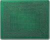
Client Die
Skylake desktop and mobile come and 2 and 4 cores. Each variant has its own die. One of the most noticeable changes on die is the amount of die space allocated to the GPU. The major components of the die is:
- System Agent
- CPU Core
- Ring bus interconnect
- Memory Controller
System Agent
The System Agent (SA) contains the Image Processing Unit (IPU), the Display Engine (DE), the I/O bus and various other shared functionality. Note that the mainstream desktop (i.e., quad-core die) does not have an IPU (The memory controller actually occupies a portion of where it would otherwise be).
Dual-Core Die

.png)
Quad-Core Die

.png)
Core
Skylake Client models come in either 2x core or 4x core setup.
- ~3.95 mm x ~2.21 mm
- ~8.73 mm²

.png)
Core Group
Client models come in groups of 2 or 4 cores. (die sizes includes the dark silicon space where the L3 ends).
- 2-cores group:
- ~8.91 mm x ~2.845 mm
- ~25.347 mm²

- 4-core group
- ~8.844 mm x 5.694 mm
- ~50.354 mm²

Integrated Graphics
The integrated graphics takes up the largest portion of the die. The normal dual-core and quad-core dies come with 24 EU Gen9.5 GPU (with 12 units disabled on the low end models).

.png)
Dual-core
Die shot of the dual-core GT2 Skylake processors. Those are found in mobile models, and entry-level/budget processors:
- 14 nm process
- 11 metal layers
- ~1,750,000,000 transistors
- ~9.57 mm x ~10.3 mm
- ~98.57 mm² die size
- 2 CPU cores + 24 GPU EUs
.png)
_(annotated).png)
Quad-core
Die shot of the quad-core GT2 Skyllake processors. Those are found in almost all mainstream desktop processors.
- 14 nm process
- 11 metal layers
- ~122 mm² die size
- 4 CPU cores + 24 GPU EUs
.png)
_(annotated).png)
Server Die

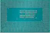
Skylake Server class models and high-end desktop (HEDT) consist of 3 different dies: Low Core Count (LCC), High Core Count (HCC), and Extreme Core Count (XCC).
Low Core Count (LCC)
- 14 nm process
- ? metal layers
- ~22.26 mm x ~14.62 mm
- ~325.44 mm² die size
- 10 cores
High Core Count (HCC)
Die shot of the octadeca core HEDT Skylake X processors.
- 14 nm process
- ? metal layers
- ? mm² die size
- 18 cores
.png)
| |
Preliminary Data! Information presented in this article deal with future products, data, features, and specifications that have yet to be finalized, announced, or released. Information may be incomplete and can change by final release. |
_(annotated).png)
Extreme Core Count (XCC)
- 14 nm process
- ? metal layers
- ? mm² die size
- 28 cores

| |
Preliminary Data! Information presented in this article deal with future products, data, features, and specifications that have yet to be finalized, announced, or released. Information may be incomplete and can change by final release. |
.png)
.png)
All Skylake Chips
| List of Skylake Processors | |||||||||||||||||||||||||
|---|---|---|---|---|---|---|---|---|---|---|---|---|---|---|---|---|---|---|---|---|---|---|---|---|---|
| Main processor | Turbo Boost | Mem | IGP | Major Feature Diff | |||||||||||||||||||||
| Model | Launched | Price | Family | Core Name | Cores | Threads | L2$ | L3$ | TDP | Frequency | 1 Core | 2 Cores | 3 Cores | 4 Cores | Max Mem | GPU | Frequency | Turbo | Turbo | SMT | AVX2 | TXT | TSX | vPro | |
| Uniprocessors | |||||||||||||||||||||||||
| 3855U | 27 December 2015 | $ 107.00 € 96.30 £ 86.67 ¥ 11,056.31 | Celeron | Skylake U | 2 | 2 | 0.5 MiB 512 KiB 524,288 B 4.882812e-4 GiB | 2 MiB 2,048 KiB 2,097,152 B 0.00195 GiB | 15 W 15,000 mW 0.0201 hp 0.015 kW | 1.6 GHz 1,600 MHz 1,600,000 kHz | 32 GiB 32,768 MiB 33,554,432 KiB 34,359,738,368 B 0.0313 TiB | HD Graphics 510 | 300 MHz 0.3 GHz 300,000 KHz | 900 MHz 0.9 GHz 900,000 KHz | ✘ | ✘ | ✘ | ✘ | ✘ | ✘ | |||||
| 3955U | 27 December 2015 | $ 107.00 € 96.30 £ 86.67 ¥ 11,056.31 | Celeron | Skylake U | 2 | 2 | 0.5 MiB 512 KiB 524,288 B 4.882812e-4 GiB | 2 MiB 2,048 KiB 2,097,152 B 0.00195 GiB | 15 W 15,000 mW 0.0201 hp 0.015 kW | 2 GHz 2,000 MHz 2,000,000 kHz | 32 GiB 32,768 MiB 33,554,432 KiB 34,359,738,368 B 0.0313 TiB | HD Graphics 510 | 300 MHz 0.3 GHz 300,000 KHz | 900 MHz 0.9 GHz 900,000 KHz | ✘ | ✘ | ✘ | ✘ | ✘ | ✘ | |||||
| G3900 | 19 October 2015 | $ 42.00 € 37.80 £ 34.02 ¥ 4,339.86 | Celeron | Skylake S | 2 | 2 | 0.5 MiB 512 KiB 524,288 B 4.882812e-4 GiB | 2 MiB 2,048 KiB 2,097,152 B 0.00195 GiB | 51 W 51,000 mW 0.0684 hp 0.051 kW | 2.8 GHz 2,800 MHz 2,800,000 kHz | 64 GiB 65,536 MiB 67,108,864 KiB 68,719,476,736 B 0.0625 TiB | HD Graphics 510 | 350 MHz 0.35 GHz 350,000 KHz | 950 MHz 0.95 GHz 950,000 KHz | ✘ | ✘ | ✔ | ✘ | ✘ | ✘ | |||||
| G3900E | 2 January 2016 | $ 107.00 € 96.30 £ 86.67 ¥ 11,056.31 | Celeron | Skylake H | 2 | 2 | 0.5 MiB 512 KiB 524,288 B 4.882812e-4 GiB | 2 MiB 2,048 KiB 2,097,152 B 0.00195 GiB | 35 W 35,000 mW 0.0469 hp 0.035 kW | 2.4 GHz 2,400 MHz 2,400,000 kHz | 64 GiB 65,536 MiB 67,108,864 KiB 68,719,476,736 B 0.0625 TiB | HD Graphics 510 | 350 MHz 0.35 GHz 350,000 KHz | 950 MHz 0.95 GHz 950,000 KHz | ✘ | ✘ | ✘ | ✘ | ✘ | ✘ | |||||
| G3900T | 19 October 2015 | Celeron | Skylake S | 2 | 2 | 0.5 MiB 512 KiB 524,288 B 4.882812e-4 GiB | 2 MiB 2,048 KiB 2,097,152 B 0.00195 GiB | 35 W 35,000 mW 0.0469 hp 0.035 kW | 2.6 GHz 2,600 MHz 2,600,000 kHz | 64 GiB 65,536 MiB 67,108,864 KiB 68,719,476,736 B 0.0625 TiB | HD Graphics 510 | 350 MHz 0.35 GHz 350,000 KHz | 950 MHz 0.95 GHz 950,000 KHz | ✘ | ✘ | ✔ | ✘ | ✘ | ✘ | ||||||
| G3900TE | 19 October 2015 | $ 42.00 € 37.80 £ 34.02 ¥ 4,339.86 | Celeron | Skylake S | 2 | 2 | 0.5 MiB 512 KiB 524,288 B 4.882812e-4 GiB | 2 MiB 2,048 KiB 2,097,152 B 0.00195 GiB | 35 W 35,000 mW 0.0469 hp 0.035 kW | 2.3 GHz 2,300 MHz 2,300,000 kHz | 64 GiB 65,536 MiB 67,108,864 KiB 68,719,476,736 B 0.0625 TiB | HD Graphics 510 | 350 MHz 0.35 GHz 350,000 KHz | 950 MHz 0.95 GHz 950,000 KHz | ✘ | ✘ | ✔ | ✘ | ✘ | ✘ | |||||
| G3902E | 2 January 2016 | $ 107.00 € 96.30 £ 86.67 ¥ 11,056.31 | Celeron | Skylake H | 2 | 2 | 0.5 MiB 512 KiB 524,288 B 4.882812e-4 GiB | 2 MiB 2,048 KiB 2,097,152 B 0.00195 GiB | 25 W 25,000 mW 0.0335 hp 0.025 kW | 1.6 GHz 1,600 MHz 1,600,000 kHz | 64 GiB 65,536 MiB 67,108,864 KiB 68,719,476,736 B 0.0625 TiB | HD Graphics 510 | 350 MHz 0.35 GHz 350,000 KHz | 950 MHz 0.95 GHz 950,000 KHz | ✘ | ✘ | ✘ | ✘ | ✘ | ✘ | |||||
| G3920 | 19 October 2015 | $ 52.00 € 46.80 £ 42.12 ¥ 5,373.16 | Celeron | Skylake S | 2 | 2 | 0.5 MiB 512 KiB 524,288 B 4.882812e-4 GiB | 2 MiB 2,048 KiB 2,097,152 B 0.00195 GiB | 51 W 51,000 mW 0.0684 hp 0.051 kW | 2.9 GHz 2,900 MHz 2,900,000 kHz | 64 GiB 65,536 MiB 67,108,864 KiB 68,719,476,736 B 0.0625 TiB | HD Graphics 510 | 350 MHz 0.35 GHz 350,000 KHz | 950 MHz 0.95 GHz 950,000 KHz | ✘ | ✘ | ✔ | ✘ | ✘ | ✘ | |||||
| i3-6006U | 10 November 2016 | $ 281.00 € 252.90 £ 227.61 ¥ 29,035.73 | Core i3 | Skylake U | 2 | 4 | 0.5 MiB 512 KiB 524,288 B 4.882812e-4 GiB | 3 MiB 3,072 KiB 3,145,728 B 0.00293 GiB | 15 W 15,000 mW 0.0201 hp 0.015 kW | 2 GHz 2,000 MHz 2,000,000 kHz | 32 GiB 32,768 MiB 33,554,432 KiB 34,359,738,368 B 0.0313 TiB | HD Graphics 520 | 300 MHz 0.3 GHz 300,000 KHz | 900 MHz 0.9 GHz 900,000 KHz | ✘ | ✔ | ✔ | ✘ | ✘ | ✘ | |||||
| i3-6098P | 27 December 2015 | $ 117.00 € 105.30 £ 94.77 ¥ 12,089.61 | Core i3 | Skylake S | 2 | 4 | 0.5 MiB 512 KiB 524,288 B 4.882812e-4 GiB | 3 MiB 3,072 KiB 3,145,728 B 0.00293 GiB | 54 W 54,000 mW 0.0724 hp 0.054 kW | 3.6 GHz 3,600 MHz 3,600,000 kHz | 64 GiB 65,536 MiB 67,108,864 KiB 68,719,476,736 B 0.0625 TiB | HD Graphics 510 | 350 MHz 0.35 GHz 350,000 KHz | 1,050 MHz 1.05 GHz 1,050,000 KHz | ✘ | ✔ | ✔ | ✘ | ✘ | ✘ | |||||
| i3-6100 | 27 September 2015 | $ 117.00 € 105.30 £ 94.77 ¥ 12,089.61 | Core i3 | Skylake S | 2 | 4 | 0.5 MiB 512 KiB 524,288 B 4.882812e-4 GiB | 3 MiB 3,072 KiB 3,145,728 B 0.00293 GiB | 51 W 51,000 mW 0.0684 hp 0.051 kW | 3.7 GHz 3,700 MHz 3,700,000 kHz | 64 GiB 65,536 MiB 67,108,864 KiB 68,719,476,736 B 0.0625 TiB | HD Graphics 530 | 350 MHz 0.35 GHz 350,000 KHz | 1,050 MHz 1.05 GHz 1,050,000 KHz | ✘ | ✔ | ✔ | ✘ | ✘ | ✘ | |||||
| i3-6100E | 12 October 2015 | $ 225.00 € 202.50 £ 182.25 ¥ 23,249.25 | Core i3 | Skylake H | 2 | 4 | 0.5 MiB 512 KiB 524,288 B 4.882812e-4 GiB | 3 MiB 3,072 KiB 3,145,728 B 0.00293 GiB | 35 W 35,000 mW 0.0469 hp 0.035 kW | 2.7 GHz 2,700 MHz 2,700,000 kHz | 64 GiB 65,536 MiB 67,108,864 KiB 68,719,476,736 B 0.0625 TiB | HD Graphics 530 | 350 MHz 0.35 GHz 350,000 KHz | 950 MHz 0.95 GHz 950,000 KHz | ✘ | ✔ | ✔ | ✘ | ✔ | ✘ | |||||
| i3-6100H | 27 September 2015 | $ 225.00 € 202.50 £ 182.25 ¥ 23,249.25 | Core i3 | Skylake H | 2 | 4 | 0.5 MiB 512 KiB 524,288 B 4.882812e-4 GiB | 3 MiB 3,072 KiB 3,145,728 B 0.00293 GiB | 35 W 35,000 mW 0.0469 hp 0.035 kW | 2.7 GHz 2,700 MHz 2,700,000 kHz | 64 GiB 65,536 MiB 67,108,864 KiB 68,719,476,736 B 0.0625 TiB | HD Graphics 530 | 350 MHz 0.35 GHz 350,000 KHz | 900 MHz 0.9 GHz 900,000 KHz | ✘ | ✔ | ✔ | ✘ | ✘ | ✘ | |||||
| i3-6100T | 27 September 2015 | $ 117.00 € 105.30 £ 94.77 ¥ 12,089.61 | Core i3 | Skylake S | 2 | 4 | 0.5 MiB 512 KiB 524,288 B 4.882812e-4 GiB | 3 MiB 3,072 KiB 3,145,728 B 0.00293 GiB | 35 W 35,000 mW 0.0469 hp 0.035 kW | 3.2 GHz 3,200 MHz 3,200,000 kHz | 64 GiB 65,536 MiB 67,108,864 KiB 68,719,476,736 B 0.0625 TiB | HD Graphics 530 | 350 MHz 0.35 GHz 350,000 KHz | 950 MHz 0.95 GHz 950,000 KHz | ✘ | ✔ | ✔ | ✘ | ✘ | ✘ | |||||
| i3-6100TE | 12 October 2015 | $ 117.00 € 105.30 £ 94.77 ¥ 12,089.61 | Core i3 | Skylake S | 2 | 4 | 0.5 MiB 512 KiB 524,288 B 4.882812e-4 GiB | 4 MiB 4,096 KiB 4,194,304 B 0.00391 GiB | 35 W 35,000 mW 0.0469 hp 0.035 kW | 2.7 GHz 2,700 MHz 2,700,000 kHz | 64 GiB 65,536 MiB 67,108,864 KiB 68,719,476,736 B 0.0625 TiB | HD Graphics 530 | 350 MHz 0.35 GHz 350,000 KHz | 1,000 MHz 1 GHz 1,000,000 KHz | ✘ | ✔ | ✔ | ✘ | ✘ | ✘ | |||||
| i3-6100U | 27 September 2015 | $ 281.00 € 252.90 £ 227.61 ¥ 29,035.73 | Core i3 | Skylake U | 2 | 4 | 0.5 MiB 512 KiB 524,288 B 4.882812e-4 GiB | 3 MiB 3,072 KiB 3,145,728 B 0.00293 GiB | 15 W 15,000 mW 0.0201 hp 0.015 kW | 2.3 GHz 2,300 MHz 2,300,000 kHz | 32 GiB 32,768 MiB 33,554,432 KiB 34,359,738,368 B 0.0313 TiB | HD Graphics 520 | 300 MHz 0.3 GHz 300,000 KHz | 1,000 MHz 1 GHz 1,000,000 KHz | ✘ | ✔ | ✔ | ✘ | ✘ | ✘ | |||||
| i3-6102E | 12 October 2015 | $ 225.00 € 202.50 £ 182.25 ¥ 23,249.25 | Core i3 | Skylake H | 2 | 4 | 0.5 MiB 512 KiB 524,288 B 4.882812e-4 GiB | 3 MiB 3,072 KiB 3,145,728 B 0.00293 GiB | 25 W 25,000 mW 0.0335 hp 0.025 kW | 1.9 GHz 1,900 MHz 1,900,000 kHz | 64 GiB 65,536 MiB 67,108,864 KiB 68,719,476,736 B 0.0625 TiB | HD Graphics 530 | 350 MHz 0.35 GHz 350,000 KHz | 950 MHz 0.95 GHz 950,000 KHz | ✘ | ✔ | ✔ | ✘ | ✔ | ✘ | |||||
| i3-6120T | Core i3 | Skylake S | 2 | 4 | 0.5 MiB 512 KiB 524,288 B 4.882812e-4 GiB | 3 MiB 3,072 KiB 3,145,728 B 0.00293 GiB | 35 W 35,000 mW 0.0469 hp 0.035 kW | 64 GiB 65,536 MiB 67,108,864 KiB 68,719,476,736 B 0.0625 TiB | HD Graphics 530 | 350 MHz 0.35 GHz 350,000 KHz | 950 MHz 0.95 GHz 950,000 KHz | ✘ | ✔ | ✔ | ✘ | ✘ | ✘ | ||||||||
| i3-6157U | June 2016 | $ 304.00 € 273.60 £ 246.24 ¥ 31,412.32 | Core i3 | Skylake U | 2 | 4 | 0.5 MiB 512 KiB 524,288 B 4.882812e-4 GiB | 3 MiB 3,072 KiB 3,145,728 B 0.00293 GiB | 28 W 28,000 mW 0.0375 hp 0.028 kW | 2.4 GHz 2,400 MHz 2,400,000 kHz | 32 GiB 32,768 MiB 33,554,432 KiB 34,359,738,368 B 0.0313 TiB | Iris Graphics 550 | 300 MHz 0.3 GHz 300,000 KHz | 1,000 MHz 1 GHz 1,000,000 KHz | ✘ | ✔ | ✔ | ✘ | ✘ | ✘ | |||||
| i3-6167U | 27 September 2015 | $ 304.00 € 273.60 £ 246.24 ¥ 31,412.32 | Core i3 | Skylake U | 2 | 4 | 0.5 MiB 512 KiB 524,288 B 4.882812e-4 GiB | 3 MiB 3,072 KiB 3,145,728 B 0.00293 GiB | 28 W 28,000 mW 0.0375 hp 0.028 kW | 2.7 GHz 2,700 MHz 2,700,000 kHz | 32 GiB 32,768 MiB 33,554,432 KiB 34,359,738,368 B 0.0313 TiB | Iris Graphics 550 | 300 MHz 0.3 GHz 300,000 KHz | 1,000 MHz 1 GHz 1,000,000 KHz | ✘ | ✔ | ✔ | ✘ | ✘ | ✘ | |||||
| i3-6300 | 27 September 2015 | $ 147.00 € 132.30 £ 119.07 ¥ 15,189.51 | Core i3 | Skylake S | 2 | 4 | 0.5 MiB 512 KiB 524,288 B 4.882812e-4 GiB | 4 MiB 4,096 KiB 4,194,304 B 0.00391 GiB | 51 W 51,000 mW 0.0684 hp 0.051 kW | 3.8 GHz 3,800 MHz 3,800,000 kHz | 64 GiB 65,536 MiB 67,108,864 KiB 68,719,476,736 B 0.0625 TiB | HD Graphics 530 | 350 MHz 0.35 GHz 350,000 KHz | 1,150 MHz 1.15 GHz 1,150,000 KHz | ✘ | ✔ | ✔ | ✘ | ✘ | ✘ | |||||
| i3-6300T | 27 September 2015 | $ 147.00 € 132.30 £ 119.07 ¥ 15,189.51 | Core i3 | Skylake S | 2 | 4 | 0.5 MiB 512 KiB 524,288 B 4.882812e-4 GiB | 4 MiB 4,096 KiB 4,194,304 B 0.00391 GiB | 35 W 35,000 mW 0.0469 hp 0.035 kW | 3.3 GHz 3,300 MHz 3,300,000 kHz | 64 GiB 65,536 MiB 67,108,864 KiB 68,719,476,736 B 0.0625 TiB | HD Graphics 530 | 350 MHz 0.35 GHz 350,000 KHz | 950 MHz 0.95 GHz 950,000 KHz | ✘ | ✔ | ✔ | ✘ | ✘ | ✘ | |||||
| i3-6320 | 27 September 2015 | $ 157.00 € 141.30 £ 127.17 ¥ 16,222.81 | Core i3 | Skylake S | 2 | 4 | 0.5 MiB 512 KiB 524,288 B 4.882812e-4 GiB | 4 MiB 4,096 KiB 4,194,304 B 0.00391 GiB | 51 W 51,000 mW 0.0684 hp 0.051 kW | 3.9 GHz 3,900 MHz 3,900,000 kHz | 64 GiB 65,536 MiB 67,108,864 KiB 68,719,476,736 B 0.0625 TiB | HD Graphics 530 | 350 MHz 0.35 GHz 350,000 KHz | 1,150 MHz 1.15 GHz 1,150,000 KHz | ✘ | ✔ | ✔ | ✘ | ✘ | ✘ | |||||
| i3-6320T | Core i3 | Skylake S | 2 | 4 | 0.5 MiB 512 KiB 524,288 B 4.882812e-4 GiB | 4 MiB 4,096 KiB 4,194,304 B 0.00391 GiB | 35 W 35,000 mW 0.0469 hp 0.035 kW | 64 GiB 65,536 MiB 67,108,864 KiB 68,719,476,736 B 0.0625 TiB | HD Graphics 530 | 350 MHz 0.35 GHz 350,000 KHz | 950 MHz 0.95 GHz 950,000 KHz | ✘ | ✔ | ✔ | ✘ | ✘ | ✘ | ||||||||
| i5-6198DU | 27 December 2015 | Core i5 | Skylake U | 2 | 4 | 0.5 MiB 512 KiB 524,288 B 4.882812e-4 GiB | 3 MiB 3,072 KiB 3,145,728 B 0.00293 GiB | 15 W 15,000 mW 0.0201 hp 0.015 kW | 2.3 GHz 2,300 MHz 2,300,000 kHz | 2.8 GHz 2,800 MHz 2,800,000 kHz | 32 GiB 32,768 MiB 33,554,432 KiB 34,359,738,368 B 0.0313 TiB | HD Graphics 510 | 300 MHz 0.3 GHz 300,000 KHz | 1,000 MHz 1 GHz 1,000,000 KHz | ✔ | ✔ | ✔ | ✘ | ✘ | ✘ | |||||
| i5-6200U | 27 September 2015 | $ 281.00 € 252.90 £ 227.61 ¥ 29,035.73 | Core i5 | Skylake U | 2 | 4 | 0.5 MiB 512 KiB 524,288 B 4.882812e-4 GiB | 3 MiB 3,072 KiB 3,145,728 B 0.00293 GiB | 15 W 15,000 mW 0.0201 hp 0.015 kW | 2.3 GHz 2,300 MHz 2,300,000 kHz | 2.8 GHz 2,800 MHz 2,800,000 kHz | 2.7 GHz 2,700 MHz 2,700,000 kHz | 32 GiB 32,768 MiB 33,554,432 KiB 34,359,738,368 B 0.0313 TiB | HD Graphics 520 | 300 MHz 0.3 GHz 300,000 KHz | 1,000 MHz 1 GHz 1,000,000 KHz | ✔ | ✔ | ✔ | ✘ | ✘ | ✘ | |||
| i5-6260U | 27 September 2015 | $ 304.00 € 273.60 £ 246.24 ¥ 31,412.32 | Core i5 | Skylake U | 2 | 4 | 0.5 MiB 512 KiB 524,288 B 4.882812e-4 GiB | 4 MiB 4,096 KiB 4,194,304 B 0.00391 GiB | 15 W 15,000 mW 0.0201 hp 0.015 kW | 1.8 GHz 1,800 MHz 1,800,000 kHz | 2.9 GHz 2,900 MHz 2,900,000 kHz | 2.7 GHz 2,700 MHz 2,700,000 kHz | 32 GiB 32,768 MiB 33,554,432 KiB 34,359,738,368 B 0.0313 TiB | Iris Graphics 540 | 300 MHz 0.3 GHz 300,000 KHz | 950 MHz 0.95 GHz 950,000 KHz | ✔ | ✔ | ✔ | ✘ | ✘ | ✘ | |||
| i5-6267U | 27 September 2015 | $ 304.00 € 273.60 £ 246.24 ¥ 31,412.32 | Core i5 | Skylake U | 2 | 4 | 0.5 MiB 512 KiB 524,288 B 4.882812e-4 GiB | 4 MiB 4,096 KiB 4,194,304 B 0.00391 GiB | 28 W 28,000 mW 0.0375 hp 0.028 kW | 2.9 GHz 2,900 MHz 2,900,000 kHz | 3.3 GHz 3,300 MHz 3,300,000 kHz | 3.1 GHz 3,100 MHz 3,100,000 kHz | 32 GiB 32,768 MiB 33,554,432 KiB 34,359,738,368 B 0.0313 TiB | Iris Graphics 550 | 300 MHz 0.3 GHz 300,000 KHz | 1,050 MHz 1.05 GHz 1,050,000 KHz | ✔ | ✔ | ✔ | ✘ | ✘ | ✘ | |||
| i5-6287U | 27 September 2015 | $ 304.00 € 273.60 £ 246.24 ¥ 31,412.32 | Core i5 | Skylake U | 2 | 4 | 0.5 MiB 512 KiB 524,288 B 4.882812e-4 GiB | 4 MiB 4,096 KiB 4,194,304 B 0.00391 GiB | 28 W 28,000 mW 0.0375 hp 0.028 kW | 3.1 GHz 3,100 MHz 3,100,000 kHz | 3.5 GHz 3,500 MHz 3,500,000 kHz | 3.3 GHz 3,300 MHz 3,300,000 kHz | 32 GiB 32,768 MiB 33,554,432 KiB 34,359,738,368 B 0.0313 TiB | Iris Graphics 550 | 300 MHz 0.3 GHz 300,000 KHz | 1,100 MHz 1.1 GHz 1,100,000 KHz | ✔ | ✔ | ✔ | ✘ | ✘ | ✘ | |||
| i5-6300HQ | 27 September 2015 | $ 250.00 € 225.00 £ 202.50 ¥ 25,832.50 | Core i5 | Skylake H | 4 | 4 | 1 MiB 1,024 KiB 1,048,576 B 9.765625e-4 GiB | 6 MiB 6,144 KiB 6,291,456 B 0.00586 GiB | 45 W 45,000 mW 0.0603 hp 0.045 kW | 2.3 GHz 2,300 MHz 2,300,000 kHz | 3.2 GHz 3,200 MHz 3,200,000 kHz | 3 GHz 3,000 MHz 3,000,000 kHz | 2.9 GHz 2,900 MHz 2,900,000 kHz | 2.8 GHz 2,800 MHz 2,800,000 kHz | 64 GiB 65,536 MiB 67,108,864 KiB 68,719,476,736 B 0.0625 TiB | HD Graphics 530 | 350 MHz 0.35 GHz 350,000 KHz | 950 MHz 0.95 GHz 950,000 KHz | ✔ | ✘ | ✔ | ✘ | ✔ | ✘ | |
| i5-6300U | 27 September 2015 | $ 281.00 € 252.90 £ 227.61 ¥ 29,035.73 | Core i5 | Skylake U | 2 | 4 | 0.5 MiB 512 KiB 524,288 B 4.882812e-4 GiB | 3 MiB 3,072 KiB 3,145,728 B 0.00293 GiB | 15 W 15,000 mW 0.0201 hp 0.015 kW | 2.4 GHz 2,400 MHz 2,400,000 kHz | 3 GHz 3,000 MHz 3,000,000 kHz | 2.9 GHz 2,900 MHz 2,900,000 kHz | 32 GiB 32,768 MiB 33,554,432 KiB 34,359,738,368 B 0.0313 TiB | HD Graphics 520 | 300 MHz 0.3 GHz 300,000 KHz | 1,000 MHz 1 GHz 1,000,000 KHz | ✔ | ✔ | ✔ | ✔ | ✔ | ✔ | |||
| i5-6350HQ | 2 January 2016 | $ 306.00 € 275.40 £ 247.86 ¥ 31,618.98 | Core i5 | Skylake H | 4 | 4 | 1 MiB 1,024 KiB 1,048,576 B 9.765625e-4 GiB | 6 MiB 6,144 KiB 6,291,456 B 0.00586 GiB | 45 W 45,000 mW 0.0603 hp 0.045 kW | 2.3 GHz 2,300 MHz 2,300,000 kHz | 3.2 GHz 3,200 MHz 3,200,000 kHz | 64 GiB 65,536 MiB 67,108,864 KiB 68,719,476,736 B 0.0625 TiB | Iris Pro Graphics 580 | 350 MHz 0.35 GHz 350,000 KHz | 900 MHz 0.9 GHz 900,000 KHz | ✔ | ✘ | ✔ | ✘ | ✘ | ✘ | ||||
| i5-6360U | 27 September 2015 | $ 304.00 € 273.60 £ 246.24 ¥ 31,412.32 | Core i5 | Skylake U | 2 | 4 | 0.5 MiB 512 KiB 524,288 B 4.882812e-4 GiB | 4 MiB 4,096 KiB 4,194,304 B 0.00391 GiB | 15 W 15,000 mW 0.0201 hp 0.015 kW | 2 GHz 2,000 MHz 2,000,000 kHz | 3.1 GHz 3,100 MHz 3,100,000 kHz | 2.9 GHz 2,900 MHz 2,900,000 kHz | 32 GiB 32,768 MiB 33,554,432 KiB 34,359,738,368 B 0.0313 TiB | Iris Graphics 540 | 300 MHz 0.3 GHz 300,000 KHz | 1,000 MHz 1 GHz 1,000,000 KHz | ✔ | ✔ | ✔ | ✔ | ✔ | ✔ | |||
| i5-6400 | 27 September 2015 | $ 187.00 € 168.30 £ 151.47 ¥ 19,322.71 | Core i5 | Skylake S | 4 | 4 | 1 MiB 1,024 KiB 1,048,576 B 9.765625e-4 GiB | 6 MiB 6,144 KiB 6,291,456 B 0.00586 GiB | 65 W 65,000 mW 0.0872 hp 0.065 kW | 2.7 GHz 2,700 MHz 2,700,000 kHz | 3.3 GHz 3,300 MHz 3,300,000 kHz | 3.3 GHz 3,300 MHz 3,300,000 kHz | 3.2 GHz 3,200 MHz 3,200,000 kHz | 3.1 GHz 3,100 MHz 3,100,000 kHz | 64 GiB 65,536 MiB 67,108,864 KiB 68,719,476,736 B 0.0625 TiB | HD Graphics 530 | 350 MHz 0.35 GHz 350,000 KHz | 950 MHz 0.95 GHz 950,000 KHz | ✔ | ✘ | ✔ | ✘ | ✘ | ✘ | |
| i5-6400T | 27 September 2015 | $ 182.00 € 163.80 £ 147.42 ¥ 18,806.06 | Core i5 | Skylake S | 4 | 4 | 1 MiB 1,024 KiB 1,048,576 B 9.765625e-4 GiB | 6 MiB 6,144 KiB 6,291,456 B 0.00586 GiB | 35 W 35,000 mW 0.0469 hp 0.035 kW | 2.2 GHz 2,200 MHz 2,200,000 kHz | 2.8 GHz 2,800 MHz 2,800,000 kHz | 2.7 GHz 2,700 MHz 2,700,000 kHz | 2.6 GHz 2,600 MHz 2,600,000 kHz | 2.5 GHz 2,500 MHz 2,500,000 kHz | 64 GiB 65,536 MiB 67,108,864 KiB 68,719,476,736 B 0.0625 TiB | HD Graphics 530 | 350 MHz 0.35 GHz 350,000 KHz | 950 MHz 0.95 GHz 950,000 KHz | ✔ | ✘ | ✔ | ✘ | ✘ | ✘ | |
| i5-6402P | 27 December 2015 | $ 187.00 € 168.30 £ 151.47 ¥ 19,322.71 | Core i5 | Skylake S | 4 | 4 | 1 MiB 1,024 KiB 1,048,576 B 9.765625e-4 GiB | 6 MiB 6,144 KiB 6,291,456 B 0.00586 GiB | 65 W 65,000 mW 0.0872 hp 0.065 kW | 2.8 GHz 2,800 MHz 2,800,000 kHz | 3.4 GHz 3,400 MHz 3,400,000 kHz | 64 GiB 65,536 MiB 67,108,864 KiB 68,719,476,736 B 0.0625 TiB | HD Graphics 510 | 350 MHz 0.35 GHz 350,000 KHz | 950 MHz 0.95 GHz 950,000 KHz | ✔ | ✘ | ✔ | ✘ | ✘ | ✘ | ||||
| i5-6440EQ | 12 October 2015 | $ 250.00 € 225.00 £ 202.50 ¥ 25,832.50 | Core i5 | Skylake H | 4 | 4 | 1 MiB 1,024 KiB 1,048,576 B 9.765625e-4 GiB | 6 MiB 6,144 KiB 6,291,456 B 0.00586 GiB | 45 W 45,000 mW 0.0603 hp 0.045 kW | 2.7 GHz 2,700 MHz 2,700,000 kHz | 3.4 GHz 3,400 MHz 3,400,000 kHz | 3.3 GHz 3,300 MHz 3,300,000 kHz | 3.2 GHz 3,200 MHz 3,200,000 kHz | 3.1 GHz 3,100 MHz 3,100,000 kHz | 64 GiB 65,536 MiB 67,108,864 KiB 68,719,476,736 B 0.0625 TiB | HD Graphics 530 | 350 MHz 0.35 GHz 350,000 KHz | 1,000 MHz 1 GHz 1,000,000 KHz | ✔ | ✘ | ✔ | ✔ | ✔ | ✔ | |
| i5-6440HQ | 27 October 2015 | $ 250.00 € 225.00 £ 202.50 ¥ 25,832.50 | Core i5 | Skylake H | 4 | 4 | 1 MiB 1,024 KiB 1,048,576 B 9.765625e-4 GiB | 6 MiB 6,144 KiB 6,291,456 B 0.00586 GiB | 45 W 45,000 mW 0.0603 hp 0.045 kW | 2.6 GHz 2,600 MHz 2,600,000 kHz | 3.5 GHz 3,500 MHz 3,500,000 kHz | 3.3 GHz 3,300 MHz 3,300,000 kHz | 3.2 GHz 3,200 MHz 3,200,000 kHz | 3.1 GHz 3,100 MHz 3,100,000 kHz | 64 GiB 65,536 MiB 67,108,864 KiB 68,719,476,736 B 0.0625 TiB | HD Graphics 530 | 350 MHz 0.35 GHz 350,000 KHz | 950 MHz 0.95 GHz 950,000 KHz | ✔ | ✘ | ✔ | ✔ | ✔ | ✔ | |
| i5-6442EQ | 12 October 2015 | $ 250.00 € 225.00 £ 202.50 ¥ 25,832.50 | Core i5 | Skylake H | 4 | 4 | 1 MiB 1,024 KiB 1,048,576 B 9.765625e-4 GiB | 6 MiB 6,144 KiB 6,291,456 B 0.00586 GiB | 25 W 25,000 mW 0.0335 hp 0.025 kW | 1.9 GHz 1,900 MHz 1,900,000 kHz | 2.7 GHz 2,700 MHz 2,700,000 kHz | 2.6 GHz 2,600 MHz 2,600,000 kHz | 2.5 GHz 2,500 MHz 2,500,000 kHz | 2.4 GHz 2,400 MHz 2,400,000 kHz | 64 GiB 65,536 MiB 67,108,864 KiB 68,719,476,736 B 0.0625 TiB | HD Graphics 530 | 350 MHz 0.35 GHz 350,000 KHz | 1,000 MHz 1 GHz 1,000,000 KHz | ✔ | ✘ | ✔ | ✔ | ✔ | ✔ | |
| i5-6500 | 27 September 2015 | $ 202.00 € 181.80 £ 163.62 ¥ 20,872.66 | Core i5 | Skylake S | 4 | 4 | 1 MiB 1,024 KiB 1,048,576 B 9.765625e-4 GiB | 6 MiB 6,144 KiB 6,291,456 B 0.00586 GiB | 65 W 65,000 mW 0.0872 hp 0.065 kW | 3.2 GHz 3,200 MHz 3,200,000 kHz | 3.6 GHz 3,600 MHz 3,600,000 kHz | 3.5 GHz 3,500 MHz 3,500,000 kHz | 3.4 GHz 3,400 MHz 3,400,000 kHz | 3.3 GHz 3,300 MHz 3,300,000 kHz | 64 GiB 65,536 MiB 67,108,864 KiB 68,719,476,736 B 0.0625 TiB | HD Graphics 530 | 350 MHz 0.35 GHz 350,000 KHz | 1,050 MHz 1.05 GHz 1,050,000 KHz | ✔ | ✘ | ✔ | ✔ | ✔ | ✔ | |
| i5-6500T | 27 September 2015 | $ 192.00 € 172.80 £ 155.52 ¥ 19,839.36 | Core i5 | Skylake S | 4 | 4 | 1 MiB 1,024 KiB 1,048,576 B 9.765625e-4 GiB | 6 MiB 6,144 KiB 6,291,456 B 0.00586 GiB | 35 W 35,000 mW 0.0469 hp 0.035 kW | 2.5 GHz 2,500 MHz 2,500,000 kHz | 3.1 GHz 3,100 MHz 3,100,000 kHz | 3 GHz 3,000 MHz 3,000,000 kHz | 2.9 GHz 2,900 MHz 2,900,000 kHz | 2.8 GHz 2,800 MHz 2,800,000 kHz | 64 GiB 65,536 MiB 67,108,864 KiB 68,719,476,736 B 0.0625 TiB | HD Graphics 530 | 350 MHz 0.35 GHz 350,000 KHz | 1,100 MHz 1.1 GHz 1,100,000 KHz | ✔ | ✘ | ✔ | ✔ | ✔ | ✔ | |
| i5-6500TE | 19 October 2015 | $ 192.00 € 172.80 £ 155.52 ¥ 19,839.36 | Core i5 | Skylake S | 4 | 4 | 1 MiB 1,024 KiB 1,048,576 B 9.765625e-4 GiB | 6 MiB 6,144 KiB 6,291,456 B 0.00586 GiB | 35 W 35,000 mW 0.0469 hp 0.035 kW | 2.3 GHz 2,300 MHz 2,300,000 kHz | 3.3 GHz 3,300 MHz 3,300,000 kHz | 3.2 GHz 3,200 MHz 3,200,000 kHz | 3.1 GHz 3,100 MHz 3,100,000 kHz | 3 GHz 3,000 MHz 3,000,000 kHz | 64 GiB 65,536 MiB 67,108,864 KiB 68,719,476,736 B 0.0625 TiB | HD Graphics 530 | 350 MHz 0.35 GHz 350,000 KHz | 1,000 MHz 1 GHz 1,000,000 KHz | ✔ | ✘ | ✔ | ✔ | ✔ | ✔ | |
| i5-6585R | 22 April 2016 | $ 255.00 € 229.50 £ 206.55 ¥ 26,349.15 | Core i5 | Skylake H | 4 | 4 | 1 MiB 1,024 KiB 1,048,576 B 9.765625e-4 GiB | 6 MiB 6,144 KiB 6,291,456 B 0.00586 GiB | 65 W 65,000 mW 0.0872 hp 0.065 kW | 2.8 GHz 2,800 MHz 2,800,000 kHz | 3.6 GHz 3,600 MHz 3,600,000 kHz | 64 GiB 65,536 MiB 67,108,864 KiB 68,719,476,736 B 0.0625 TiB | Iris Pro Graphics 580 | 350 MHz 0.35 GHz 350,000 KHz | 1,100 MHz 1.1 GHz 1,100,000 KHz | ✔ | ✘ | ✔ | ✔ | ✔ | ✘ | ||||
| i5-6600 | 27 September 2015 | $ 224.00 € 201.60 £ 181.44 ¥ 23,145.92 | Core i5 | Skylake S | 4 | 4 | 1 MiB 1,024 KiB 1,048,576 B 9.765625e-4 GiB | 6 MiB 6,144 KiB 6,291,456 B 0.00586 GiB | 65 W 65,000 mW 0.0872 hp 0.065 kW | 3.3 GHz 3,300 MHz 3,300,000 kHz | 3.9 GHz 3,900 MHz 3,900,000 kHz | 3.8 GHz 3,800 MHz 3,800,000 kHz | 3.7 GHz 3,700 MHz 3,700,000 kHz | 3.6 GHz 3,600 MHz 3,600,000 kHz | 64 GiB 65,536 MiB 67,108,864 KiB 68,719,476,736 B 0.0625 TiB | HD Graphics 530 | 350 MHz 0.35 GHz 350,000 KHz | 1,150 MHz 1.15 GHz 1,150,000 KHz | ✔ | ✘ | ✔ | ✔ | ✔ | ✔ | |
| i5-6600K | 27 September 2015 | $ 243.00 € 218.70 £ 196.83 ¥ 25,109.19 | Core i5 | Skylake S | 4 | 4 | 1 MiB 1,024 KiB 1,048,576 B 9.765625e-4 GiB | 6 MiB 6,144 KiB 6,291,456 B 0.00586 GiB | 91 W 91,000 mW 0.122 hp 0.091 kW | 3.5 GHz 3,500 MHz 3,500,000 kHz | 3.9 GHz 3,900 MHz 3,900,000 kHz | 3.8 GHz 3,800 MHz 3,800,000 kHz | 3.7 GHz 3,700 MHz 3,700,000 kHz | 3.6 GHz 3,600 MHz 3,600,000 kHz | 64 GiB 65,536 MiB 67,108,864 KiB 68,719,476,736 B 0.0625 TiB | HD Graphics 530 | 350 MHz 0.35 GHz 350,000 KHz | 1,150 MHz 1.15 GHz 1,150,000 KHz | ✔ | ✘ | ✔ | ✘ | ✔ | ✘ | |
| i5-6600T | 27 September 2015 | $ 213.00 € 191.70 £ 172.53 ¥ 22,009.29 | Core i5 | Skylake S | 4 | 4 | 1 MiB 1,024 KiB 1,048,576 B 9.765625e-4 GiB | 6 MiB 6,144 KiB 6,291,456 B 0.00586 GiB | 35 W 35,000 mW 0.0469 hp 0.035 kW | 2.7 GHz 2,700 MHz 2,700,000 kHz | 3.5 GHz 3,500 MHz 3,500,000 kHz | 3.4 GHz 3,400 MHz 3,400,000 kHz | 3.3 GHz 3,300 MHz 3,300,000 kHz | 3.3 GHz 3,300 MHz 3,300,000 kHz | 64 GiB 65,536 MiB 67,108,864 KiB 68,719,476,736 B 0.0625 TiB | HD Graphics 530 | 350 MHz 0.35 GHz 350,000 KHz | 1,100 MHz 1.1 GHz 1,100,000 KHz | ✔ | ✘ | ✔ | ✔ | ✔ | ✔ | |
| i5-6685R | 22 April 2016 | $ 288.00 € 259.20 £ 233.28 ¥ 29,759.04 | Core i5 | Skylake H | 4 | 4 | 1 MiB 1,024 KiB 1,048,576 B 9.765625e-4 GiB | 6 MiB 6,144 KiB 6,291,456 B 0.00586 GiB | 65 W 65,000 mW 0.0872 hp 0.065 kW | 3.2 GHz 3,200 MHz 3,200,000 kHz | 3.8 GHz 3,800 MHz 3,800,000 kHz | 64 GiB 65,536 MiB 67,108,864 KiB 68,719,476,736 B 0.0625 TiB | Iris Pro Graphics 580 | 350 MHz 0.35 GHz 350,000 KHz | 1,150 MHz 1.15 GHz 1,150,000 KHz | ✔ | ✘ | ✔ | ✔ | ✔ | ✘ | ||||
| i7-6498DU | 27 September 2015 | $ 393.00 € 353.70 £ 318.33 ¥ 40,608.69 | Core i7 | Skylake U | 2 | 4 | 0.5 MiB 512 KiB 524,288 B 4.882812e-4 GiB | 4 MiB 4,096 KiB 4,194,304 B 0.00391 GiB | 15 W 15,000 mW 0.0201 hp 0.015 kW | 2.5 GHz 2,500 MHz 2,500,000 kHz | 3.1 GHz 3,100 MHz 3,100,000 kHz | 32 GiB 32,768 MiB 33,554,432 KiB 34,359,738,368 B 0.0313 TiB | HD Graphics 510 | 300 MHz 0.3 GHz 300,000 KHz | 1,050 MHz 1.05 GHz 1,050,000 KHz | ✔ | ✔ | ✔ | ✘ | ✘ | ✘ | ||||
| i7-6500U | 27 September 2015 | $ 393.00 € 353.70 £ 318.33 ¥ 40,608.69 | Core i7 | Skylake U | 2 | 4 | 0.5 MiB 512 KiB 524,288 B 4.882812e-4 GiB | 4 MiB 4,096 KiB 4,194,304 B 0.00391 GiB | 15 W 15,000 mW 0.0201 hp 0.015 kW | 2.5 GHz 2,500 MHz 2,500,000 kHz | 3.1 GHz 3,100 MHz 3,100,000 kHz | 3 GHz 3,000 MHz 3,000,000 kHz | 32 GiB 32,768 MiB 33,554,432 KiB 34,359,738,368 B 0.0313 TiB | HD Graphics 520 | 300 MHz 0.3 GHz 300,000 KHz | 1,050 MHz 1.05 GHz 1,050,000 KHz | ✔ | ✔ | ✔ | ✘ | ✘ | ✘ | |||
| i7-6560U | 27 September 2015 | Core i7 | Skylake U | 2 | 4 | 0.5 MiB 512 KiB 524,288 B 4.882812e-4 GiB | 4 MiB 4,096 KiB 4,194,304 B 0.00391 GiB | 15 W 15,000 mW 0.0201 hp 0.015 kW | 2.2 GHz 2,200 MHz 2,200,000 kHz | 3.2 GHz 3,200 MHz 3,200,000 kHz | 3.1 GHz 3,100 MHz 3,100,000 kHz | 32 GiB 32,768 MiB 33,554,432 KiB 34,359,738,368 B 0.0313 TiB | Iris Graphics 540 | 300 MHz 0.3 GHz 300,000 KHz | 1,050 MHz 1.05 GHz 1,050,000 KHz | ✔ | ✔ | ✔ | ✘ | ✘ | ✘ | ||||
| i7-6567U | 27 September 2015 | Core i7 | Skylake U | 2 | 4 | 0.5 MiB 512 KiB 524,288 B 4.882812e-4 GiB | 4 MiB 4,096 KiB 4,194,304 B 0.00391 GiB | 28 W 28,000 mW 0.0375 hp 0.028 kW | 3.3 GHz 3,300 MHz 3,300,000 kHz | 3.6 GHz 3,600 MHz 3,600,000 kHz | 3.4 GHz 3,400 MHz 3,400,000 kHz | 32 GiB 32,768 MiB 33,554,432 KiB 34,359,738,368 B 0.0313 TiB | Iris Graphics 550 | 300 MHz 0.3 GHz 300,000 KHz | 1,100 MHz 1.1 GHz 1,100,000 KHz | ✔ | ✔ | ✔ | ✘ | ✘ | ✘ | ||||
| i7-6600U | 27 September 2015 | $ 393.00 € 353.70 £ 318.33 ¥ 40,608.69 | Core i7 | Skylake U | 2 | 4 | 0.5 MiB 512 KiB 524,288 B 4.882812e-4 GiB | 4 MiB 4,096 KiB 4,194,304 B 0.00391 GiB | 15 W 15,000 mW 0.0201 hp 0.015 kW | 2.6 GHz 2,600 MHz 2,600,000 kHz | 3.4 GHz 3,400 MHz 3,400,000 kHz | 3.2 GHz 3,200 MHz 3,200,000 kHz | 32 GiB 32,768 MiB 33,554,432 KiB 34,359,738,368 B 0.0313 TiB | HD Graphics 520 | 300 MHz 0.3 GHz 300,000 KHz | 1,050 MHz 1.05 GHz 1,050,000 KHz | ✔ | ✔ | ✔ | ✔ | ✔ | ✔ | |||
| i7-6650U | 27 September 2015 | $ 415.00 € 373.50 £ 336.15 ¥ 42,881.95 | Core i7 | Skylake U | 2 | 4 | 0.5 MiB 512 KiB 524,288 B 4.882812e-4 GiB | 4 MiB 4,096 KiB 4,194,304 B 0.00391 GiB | 15 W 15,000 mW 0.0201 hp 0.015 kW | 2.2 GHz 2,200 MHz 2,200,000 kHz | 3.4 GHz 3,400 MHz 3,400,000 kHz | 3.2 GHz 3,200 MHz 3,200,000 kHz | 32 GiB 32,768 MiB 33,554,432 KiB 34,359,738,368 B 0.0313 TiB | Iris Graphics 540 | 300 MHz 0.3 GHz 300,000 KHz | 1,050 MHz 1.05 GHz 1,050,000 KHz | ✔ | ✔ | ✔ | ✔ | ✔ | ✔ | |||
| i7-6660U | 20 March 2016 | $ 415.00 € 373.50 £ 336.15 ¥ 42,881.95 | Core i7 | Skylake U | 2 | 4 | 0.5 MiB 512 KiB 524,288 B 4.882812e-4 GiB | 4 MiB 4,096 KiB 4,194,304 B 0.00391 GiB | 15 W 15,000 mW 0.0201 hp 0.015 kW | 2.4 GHz 2,400 MHz 2,400,000 kHz | 3.4 GHz 3,400 MHz 3,400,000 kHz | 3.4 GHz 3,400 MHz 3,400,000 kHz | 32 GiB 32,768 MiB 33,554,432 KiB 34,359,738,368 B 0.0313 TiB | Iris Graphics 540 | 300 MHz 0.3 GHz 300,000 KHz | 1,050 MHz 1.05 GHz 1,050,000 KHz | ✔ | ✔ | ✔ | ✔ | ✔ | ✔ | |||
| i7-6700 | 27 September 2015 | $ 312.00 € 280.80 £ 252.72 ¥ 32,238.96 | Core i7 | Skylake S | 4 | 8 | 1 MiB 1,024 KiB 1,048,576 B 9.765625e-4 GiB | 8 MiB 8,192 KiB 8,388,608 B 0.00781 GiB | 65 W 65,000 mW 0.0872 hp 0.065 kW | 3.4 GHz 3,400 MHz 3,400,000 kHz | 4 GHz 4,000 MHz 4,000,000 kHz | 3.9 GHz 3,900 MHz 3,900,000 kHz | 3.8 GHz 3,800 MHz 3,800,000 kHz | 3.7 GHz 3,700 MHz 3,700,000 kHz | 64 GiB 65,536 MiB 67,108,864 KiB 68,719,476,736 B 0.0625 TiB | HD Graphics 530 | 350 MHz 0.35 GHz 350,000 KHz | 1,150 MHz 1.15 GHz 1,150,000 KHz | ✘ | ✔ | ✔ | ✔ | ✔ | ✘ | |
| i7-6700HQ | 27 September 2015 | $ 378.00 € 340.20 £ 306.18 ¥ 39,058.74 | Core i7 | Skylake H | 4 | 8 | 1 MiB 1,024 KiB 1,048,576 B 9.765625e-4 GiB | 6 MiB 6,144 KiB 6,291,456 B 0.00586 GiB | 45 W 45,000 mW 0.0603 hp 0.045 kW | 2.6 GHz 2,600 MHz 2,600,000 kHz | 3.5 GHz 3,500 MHz 3,500,000 kHz | 3.3 GHz 3,300 MHz 3,300,000 kHz | 3.2 GHz 3,200 MHz 3,200,000 kHz | 3.1 GHz 3,100 MHz 3,100,000 kHz | 64 GiB 65,536 MiB 67,108,864 KiB 68,719,476,736 B 0.0625 TiB | HD Graphics 530 | 350 MHz 0.35 GHz 350,000 KHz | 1,050 MHz 1.05 GHz 1,050,000 KHz | ✔ | ✔ | ✔ | ✘ | ✘ | ✘ | |
| i7-6700K | 27 September 2015 | $ 350.00 € 315.00 £ 283.50 ¥ 36,165.50 | Core i7 | Skylake S | 4 | 8 | 1 MiB 1,024 KiB 1,048,576 B 9.765625e-4 GiB | 8 MiB 8,192 KiB 8,388,608 B 0.00781 GiB | 91 W 91,000 mW 0.122 hp 0.091 kW | 4 GHz 4,000 MHz 4,000,000 kHz | 4.2 GHz 4,200 MHz 4,200,000 kHz | 4 GHz 4,000 MHz 4,000,000 kHz | 4 GHz 4,000 MHz 4,000,000 kHz | 4 GHz 4,000 MHz 4,000,000 kHz | 64 GiB 65,536 MiB 67,108,864 KiB 68,719,476,736 B 0.0625 TiB | HD Graphics 530 | 350 MHz 0.35 GHz 350,000 KHz | 1,150 MHz 1.15 GHz 1,150,000 KHz | ✔ | ✔ | ✔ | ✘ | ✔ | ✘ | |
| i7-6700T | 27 September 2015 | $ 303.00 € 272.70 £ 245.43 ¥ 31,308.99 | Core i7 | Skylake S | 4 | 8 | 1 MiB 1,024 KiB 1,048,576 B 9.765625e-4 GiB | 8 MiB 8,192 KiB 8,388,608 B 0.00781 GiB | 35 W 35,000 mW 0.0469 hp 0.035 kW | 2.8 GHz 2,800 MHz 2,800,000 kHz | 3.6 GHz 3,600 MHz 3,600,000 kHz | 3.5 GHz 3,500 MHz 3,500,000 kHz | 3.4 GHz 3,400 MHz 3,400,000 kHz | 3.4 GHz 3,400 MHz 3,400,000 kHz | 64 GiB 65,536 MiB 67,108,864 KiB 68,719,476,736 B 0.0625 TiB | HD Graphics 530 | 350 MHz 0.35 GHz 350,000 KHz | 1,100 MHz 1.1 GHz 1,100,000 KHz | ✔ | ✔ | ✔ | ✔ | ✔ | ✔ | |
| i7-6700TE | 19 October 2015 | $ 303.00 € 272.70 £ 245.43 ¥ 31,308.99 | Core i7 | Skylake S | 4 | 8 | 1 MiB 1,024 KiB 1,048,576 B 9.765625e-4 GiB | 8 MiB 8,192 KiB 8,388,608 B 0.00781 GiB | 35 W 35,000 mW 0.0469 hp 0.035 kW | 2.4 GHz 2,400 MHz 2,400,000 kHz | 3.4 GHz 3,400 MHz 3,400,000 kHz | 3.3 GHz 3,300 MHz 3,300,000 kHz | 3.2 GHz 3,200 MHz 3,200,000 kHz | 3.1 GHz 3,100 MHz 3,100,000 kHz | 64 GiB 65,536 MiB 67,108,864 KiB 68,719,476,736 B 0.0625 TiB | HD Graphics 530 | 350 MHz 0.35 GHz 350,000 KHz | 1,000 MHz 1 GHz 1,000,000 KHz | ✔ | ✔ | ✔ | ✔ | ✔ | ✔ | |
| i7-6770HQ | 2 January 2016 | $ 434.00 € 390.60 £ 351.54 ¥ 44,845.22 | Core i7 | Skylake H | 4 | 8 | 1 MiB 1,024 KiB 1,048,576 B 9.765625e-4 GiB | 6 MiB 6,144 KiB 6,291,456 B 0.00586 GiB | 45 W 45,000 mW 0.0603 hp 0.045 kW | 2.6 GHz 2,600 MHz 2,600,000 kHz | 3.5 GHz 3,500 MHz 3,500,000 kHz | 64 GiB 65,536 MiB 67,108,864 KiB 68,719,476,736 B 0.0625 TiB | Iris Pro Graphics 580 | 350 MHz 0.35 GHz 350,000 KHz | 950 MHz 0.95 GHz 950,000 KHz | ✔ | ✔ | ✔ | ✘ | ✘ | ✘ | ||||
| i7-6785R | 22 April 2016 | $ 370.00 € 333.00 £ 299.70 ¥ 38,232.10 | Core i7 | Skylake H | 4 | 8 | 1 MiB 1,024 KiB 1,048,576 B 9.765625e-4 GiB | 8 MiB 8,192 KiB 8,388,608 B 0.00781 GiB | 65 W 65,000 mW 0.0872 hp 0.065 kW | 3.3 GHz 3,300 MHz 3,300,000 kHz | 3.9 GHz 3,900 MHz 3,900,000 kHz | 64 GiB 65,536 MiB 67,108,864 KiB 68,719,476,736 B 0.0625 TiB | Iris Pro Graphics 580 | 350 MHz 0.35 GHz 350,000 KHz | 1,150 MHz 1.15 GHz 1,150,000 KHz | ✔ | ✔ | ✔ | ✔ | ✔ | ✘ | ||||
| i7-6820EQ | 12 October 2015 | $ 378.00 € 340.20 £ 306.18 ¥ 39,058.74 | Core i7 | Skylake H | 4 | 8 | 1 MiB 1,024 KiB 1,048,576 B 9.765625e-4 GiB | 8 MiB 8,192 KiB 8,388,608 B 0.00781 GiB | 45 W 45,000 mW 0.0603 hp 0.045 kW | 2.8 GHz 2,800 MHz 2,800,000 kHz | 3.5 GHz 3,500 MHz 3,500,000 kHz | 3.4 GHz 3,400 MHz 3,400,000 kHz | 3.3 GHz 3,300 MHz 3,300,000 kHz | 3.2 GHz 3,200 MHz 3,200,000 kHz | 64 GiB 65,536 MiB 67,108,864 KiB 68,719,476,736 B 0.0625 TiB | HD Graphics 530 | 350 MHz 0.35 GHz 350,000 KHz | 1,000 MHz 1 GHz 1,000,000 KHz | ✔ | ✔ | ✔ | ✔ | ✔ | ✔ | |
| i7-6820HK | 27 September 2015 | $ 378.00 € 340.20 £ 306.18 ¥ 39,058.74 | Core i7 | Skylake H | 4 | 8 | 1 MiB 1,024 KiB 1,048,576 B 9.765625e-4 GiB | 8 MiB 8,192 KiB 8,388,608 B 0.00781 GiB | 45 W 45,000 mW 0.0603 hp 0.045 kW | 2.7 GHz 2,700 MHz 2,700,000 kHz | 3.6 GHz 3,600 MHz 3,600,000 kHz | 3.4 GHz 3,400 MHz 3,400,000 kHz | 3.3 GHz 3,300 MHz 3,300,000 kHz | 3.2 GHz 3,200 MHz 3,200,000 kHz | 64 GiB 65,536 MiB 67,108,864 KiB 68,719,476,736 B 0.0625 TiB | HD Graphics 530 | 350 MHz 0.35 GHz 350,000 KHz | 1,050 MHz 1.05 GHz 1,050,000 KHz | ✔ | ✔ | ✔ | ✘ | ✔ | ✘ | |
| i7-6820HQ | 27 October 2015 | $ 378.00 € 340.20 £ 306.18 ¥ 39,058.74 | Core i7 | Skylake H | 4 | 8 | 1 MiB 1,024 KiB 1,048,576 B 9.765625e-4 GiB | 8 MiB 8,192 KiB 8,388,608 B 0.00781 GiB | 45 W 45,000 mW 0.0603 hp 0.045 kW | 2.7 GHz 2,700 MHz 2,700,000 kHz | 3.6 GHz 3,600 MHz 3,600,000 kHz | 3.4 GHz 3,400 MHz 3,400,000 kHz | 3.2 GHz 3,200 MHz 3,200,000 kHz | 3.2 GHz 3,200 MHz 3,200,000 kHz | 64 GiB 65,536 MiB 67,108,864 KiB 68,719,476,736 B 0.0625 TiB | HD Graphics 530 | 350 MHz 0.35 GHz 350,000 KHz | 1,050 MHz 1.05 GHz 1,050,000 KHz | ✔ | ✔ | ✔ | ✔ | ✔ | ✔ | |
| i7-6822EQ | 12 October 2015 | $ 378.00 € 340.20 £ 306.18 ¥ 39,058.74 | Core i7 | Skylake H | 4 | 8 | 1 MiB 1,024 KiB 1,048,576 B 9.765625e-4 GiB | 8 MiB 8,192 KiB 8,388,608 B 0.00781 GiB | 25 W 25,000 mW 0.0335 hp 0.025 kW | 2 GHz 2,000 MHz 2,000,000 kHz | 2.8 GHz 2,800 MHz 2,800,000 kHz | 2.7 GHz 2,700 MHz 2,700,000 kHz | 2.6 GHz 2,600 MHz 2,600,000 kHz | 2.55 GHz 2,550 MHz 2,550,000 kHz | 64 GiB 65,536 MiB 67,108,864 KiB 68,719,476,736 B 0.0625 TiB | HD Graphics 530 | 350 MHz 0.35 GHz 350,000 KHz | 1,000 MHz 1 GHz 1,000,000 KHz | ✔ | ✔ | ✔ | ✔ | ✔ | ✔ | |
| i7-6870HQ | 2 January 2016 | $ 434.00 € 390.60 £ 351.54 ¥ 44,845.22 | Core i7 | Skylake H | 4 | 8 | 1 MiB 1,024 KiB 1,048,576 B 9.765625e-4 GiB | 8 MiB 8,192 KiB 8,388,608 B 0.00781 GiB | 45 W 45,000 mW 0.0603 hp 0.045 kW | 2.7 GHz 2,700 MHz 2,700,000 kHz | 3.6 GHz 3,600 MHz 3,600,000 kHz | 64 GiB 65,536 MiB 67,108,864 KiB 68,719,476,736 B 0.0625 TiB | Iris Pro Graphics 580 | 350 MHz 0.35 GHz 350,000 KHz | 1,000 MHz 1 GHz 1,000,000 KHz | ✔ | ✔ | ✔ | ✘ | ✘ | ✘ | ||||
| i7-6920HQ | 27 October 2015 | $ 568.00 € 511.20 £ 460.08 ¥ 58,691.44 | Core i7 | Skylake H | 4 | 8 | 1 MiB 1,024 KiB 1,048,576 B 9.765625e-4 GiB | 8 MiB 8,192 KiB 8,388,608 B 0.00781 GiB | 45 W 45,000 mW 0.0603 hp 0.045 kW | 2.9 GHz 2,900 MHz 2,900,000 kHz | 3.8 GHz 3,800 MHz 3,800,000 kHz | 3.6 GHz 3,600 MHz 3,600,000 kHz | 3.5 GHz 3,500 MHz 3,500,000 kHz | 3.4 GHz 3,400 MHz 3,400,000 kHz | 64 GiB 65,536 MiB 67,108,864 KiB 68,719,476,736 B 0.0625 TiB | HD Graphics 530 | 350 MHz 0.35 GHz 350,000 KHz | 1,050 MHz 1.05 GHz 1,050,000 KHz | ✔ | ✔ | ✔ | ✔ | ✔ | ✔ | |
| i7-6970HQ | 2 January 2016 | $ 623.00 € 560.70 £ 504.63 ¥ 64,374.59 | Core i7 | Skylake H | 4 | 8 | 1 MiB 1,024 KiB 1,048,576 B 9.765625e-4 GiB | 8 MiB 8,192 KiB 8,388,608 B 0.00781 GiB | 45 W 45,000 mW 0.0603 hp 0.045 kW | 2.8 GHz 2,800 MHz 2,800,000 kHz | 3.7 GHz 3,700 MHz 3,700,000 kHz | 64 GiB 65,536 MiB 67,108,864 KiB 68,719,476,736 B 0.0625 TiB | Iris Pro Graphics 580 | 350 MHz 0.35 GHz 350,000 KHz | 1,050 MHz 1.05 GHz 1,050,000 KHz | ✔ | ✔ | ✔ | ✘ | ✘ | ✘ | ||||
| i7-7500U | 30 August 2016 | $ 393.00 € 353.70 £ 318.33 ¥ 40,608.69 | Core i7 | Kaby Lake U | 2 | 4 | 0.5 MiB 512 KiB 524,288 B 4.882812e-4 GiB | 4 MiB 4,096 KiB 4,194,304 B 0.00391 GiB | 15 W 15,000 mW 0.0201 hp 0.015 kW | 2.7 GHz 2,700 MHz 2,700,000 kHz | 3.5 GHz 3,500 MHz 3,500,000 kHz | 32 GiB 32,768 MiB 33,554,432 KiB 34,359,738,368 B 0.0313 TiB | HD Graphics 620 | 300 MHz 0.3 GHz 300,000 KHz | 1,050 MHz 1.05 GHz 1,050,000 KHz | ✔ | ✔ | ✔ | ✘ | ✘ | ✘ | ||||
| i7-8565U | 28 August 2018 | $ 409.00 € 368.10 £ 331.29 ¥ 42,261.97 | Core i7 | Whiskey Lake U | 4 | 8 | 1 MiB 1,024 KiB 1,048,576 B 9.765625e-4 GiB | 8 MiB 8,192 KiB 8,388,608 B 0.00781 GiB | 15 W 15,000 mW 0.0201 hp 0.015 kW | 1.8 GHz 1,800 MHz 1,800,000 kHz | 4.6 GHz 4,600 MHz 4,600,000 kHz | 4.5 GHz 4,500 MHz 4,500,000 kHz | 4.1 GHz 4,100 MHz 4,100,000 kHz | 32 GiB 32,768 MiB 33,554,432 KiB 34,359,738,368 B 0.0313 TiB | UHD Graphics 620 | 300 MHz 0.3 GHz 300,000 KHz | 1,150 MHz 1.15 GHz 1,150,000 KHz | ✔ | ✔ | ✔ | ✘ | ✘ | ✘ | ||
| m3-6Y30 | 27 September 2015 | $ 281.00 € 252.90 £ 227.61 ¥ 29,035.73 | Core m3 | Skylake Y | 2 | 4 | 0.5 MiB 512 KiB 524,288 B 4.882812e-4 GiB | 4 MiB 4,096 KiB 4,194,304 B 0.00391 GiB | 4.5 W 4,500 mW 0.00603 hp 0.0045 kW | 0.9 GHz 900 MHz 900,000 kHz | 2.2 GHz 2,200 MHz 2,200,000 kHz | 2 GHz 2,000 MHz 2,000,000 kHz | 16 GiB 16,384 MiB 16,777,216 KiB 17,179,869,184 B 0.0156 TiB | HD Graphics 515 | 300 MHz 0.3 GHz 300,000 KHz | 850 MHz 0.85 GHz 850,000 KHz | ✔ | ✔ | ✔ | ✘ | ✘ | ✘ | |||
| m5-6Y54 | 27 September 2015 | $ 281.00 € 252.90 £ 227.61 ¥ 29,035.73 | Core m5 | Skylake Y | 2 | 4 | 0.5 MiB 512 KiB 524,288 B 4.882812e-4 GiB | 4 MiB 4,096 KiB 4,194,304 B 0.00391 GiB | 4.5 W 4,500 mW 0.00603 hp 0.0045 kW | 1.1 GHz 1,100 MHz 1,100,000 kHz | 2.7 GHz 2,700 MHz 2,700,000 kHz | 2.4 GHz 2,400 MHz 2,400,000 kHz | 16 GiB 16,384 MiB 16,777,216 KiB 17,179,869,184 B 0.0156 TiB | HD Graphics 515 | 300 MHz 0.3 GHz 300,000 KHz | 900 MHz 0.9 GHz 900,000 KHz | ✔ | ✔ | ✔ | ✘ | ✘ | ✘ | |||
| m5-6Y57 | 27 September 2015 | $ 281.00 € 252.90 £ 227.61 ¥ 29,035.73 | Core m5 | Skylake Y | 2 | 4 | 0.5 MiB 512 KiB 524,288 B 4.882812e-4 GiB | 4 MiB 4,096 KiB 4,194,304 B 0.00391 GiB | 4.5 W 4,500 mW 0.00603 hp 0.0045 kW | 1.1 GHz 1,100 MHz 1,100,000 kHz | 2.8 GHz 2,800 MHz 2,800,000 kHz | 2.4 GHz 2,400 MHz 2,400,000 kHz | 16 GiB 16,384 MiB 16,777,216 KiB 17,179,869,184 B 0.0156 TiB | HD Graphics 515 | 300 MHz 0.3 GHz 300,000 KHz | 900 MHz 0.9 GHz 900,000 KHz | ✔ | ✔ | ✔ | ✔ | ✔ | ✔ | |||
| m7-6Y75 | 27 September 2015 | $ 393.00 € 353.70 £ 318.33 ¥ 40,608.69 | Core m7 | Skylake Y | 2 | 4 | 0.5 MiB 512 KiB 524,288 B 4.882812e-4 GiB | 4 MiB 4,096 KiB 4,194,304 B 0.00391 GiB | 4.5 W 4,500 mW 0.00603 hp 0.0045 kW | 1.2 GHz 1,200 MHz 1,200,000 kHz | 3.1 GHz 3,100 MHz 3,100,000 kHz | 2.9 GHz 2,900 MHz 2,900,000 kHz | 16 GiB 16,384 MiB 16,777,216 KiB 17,179,869,184 B 0.0156 TiB | HD Graphics 515 | 300 MHz 0.3 GHz 300,000 KHz | 1,000 MHz 1 GHz 1,000,000 KHz | ✔ | ✔ | ✔ | ✔ | ✔ | ✔ | |||
| 4405U | 3 November 2015 | $ 161.00 € 144.90 £ 130.41 ¥ 16,636.13 | Pentium | Skylake U | 2 | 4 | 0.5 MiB 512 KiB 524,288 B 4.882812e-4 GiB | 2 MiB 2,048 KiB 2,097,152 B 0.00195 GiB | 15 W 15,000 mW 0.0201 hp 0.015 kW | 2.1 GHz 2,100 MHz 2,100,000 kHz | 32 GiB 32,768 MiB 33,554,432 KiB 34,359,738,368 B 0.0313 TiB | HD Graphics 510 | 300 MHz 0.3 GHz 300,000 KHz | 950 MHz 0.95 GHz 950,000 KHz | ✘ | ✔ | ✘ | ✘ | ✘ | ✘ | |||||
| 4405Y | 3 November 2015 | $ 161.00 € 144.90 £ 130.41 ¥ 16,636.13 | Pentium | Skylake Y | 2 | 4 | 0.5 MiB 512 KiB 524,288 B 4.882812e-4 GiB | 2 MiB 2,048 KiB 2,097,152 B 0.00195 GiB | 6 W 6,000 mW 0.00805 hp 0.006 kW | 1.5 GHz 1,500 MHz 1,500,000 kHz | 16 GiB 16,384 MiB 16,777,216 KiB 17,179,869,184 B 0.0156 TiB | HD Graphics 515 | 300 MHz 0.3 GHz 300,000 KHz | 800 MHz 0.8 GHz 800,000 KHz | ✘ | ✔ | ✘ | ✘ | ✘ | ✘ | |||||
| G4400 | 27 September 2015 | $ 64.00 € 57.60 £ 51.84 ¥ 6,613.12 | Pentium | Skylake S | 2 | 2 | 0.5 MiB 512 KiB 524,288 B 4.882812e-4 GiB | 3 MiB 3,072 KiB 3,145,728 B 0.00293 GiB | 54 W 54,000 mW 0.0724 hp 0.054 kW | 3.3 GHz 3,300 MHz 3,300,000 kHz | 64 GiB 65,536 MiB 67,108,864 KiB 68,719,476,736 B 0.0625 TiB | HD Graphics 510 | 350 MHz 0.35 GHz 350,000 KHz | 1,000 MHz 1 GHz 1,000,000 KHz | ✘ | ✘ | ✔ | ✘ | ✘ | ✘ | |||||
| G4400T | 27 September 2015 | $ 64.00 € 57.60 £ 51.84 ¥ 6,613.12 | Pentium | Skylake S | 2 | 2 | 0.5 MiB 512 KiB 524,288 B 4.882812e-4 GiB | 3 MiB 3,072 KiB 3,145,728 B 0.00293 GiB | 35 W 35,000 mW 0.0469 hp 0.035 kW | 2.9 GHz 2,900 MHz 2,900,000 kHz | 64 GiB 65,536 MiB 67,108,864 KiB 68,719,476,736 B 0.0625 TiB | HD Graphics 510 | 350 MHz 0.35 GHz 350,000 KHz | 950 MHz 0.95 GHz 950,000 KHz | ✘ | ✘ | ✔ | ✘ | ✘ | ✘ | |||||
| G4400TE | 9 December 2015 | $ 64.00 € 57.60 £ 51.84 ¥ 6,613.12 | Pentium | Skylake S | 2 | 2 | 0.5 MiB 512 KiB 524,288 B 4.882812e-4 GiB | 3 MiB 3,072 KiB 3,145,728 B 0.00293 GiB | 35 W 35,000 mW 0.0469 hp 0.035 kW | 2.4 GHz 2,400 MHz 2,400,000 kHz | 64 GiB 65,536 MiB 67,108,864 KiB 68,719,476,736 B 0.0625 TiB | HD Graphics 510 | 350 MHz 0.35 GHz 350,000 KHz | 950 MHz 0.95 GHz 950,000 KHz | ✘ | ✘ | ✔ | ✘ | ✘ | ✘ | |||||
| G4500 | 27 September 2015 | $ 82.00 € 73.80 £ 66.42 ¥ 8,473.06 | Pentium | Skylake S | 2 | 2 | 0.5 MiB 512 KiB 524,288 B 4.882812e-4 GiB | 3 MiB 3,072 KiB 3,145,728 B 0.00293 GiB | 51 W 51,000 mW 0.0684 hp 0.051 kW | 3.5 GHz 3,500 MHz 3,500,000 kHz | 64 GiB 65,536 MiB 67,108,864 KiB 68,719,476,736 B 0.0625 TiB | HD Graphics 530 | 350 MHz 0.35 GHz 350,000 KHz | 1,050 MHz 1.05 GHz 1,050,000 KHz | ✘ | ✘ | ✔ | ✘ | ✘ | ✘ | |||||
| G4500T | 27 September 2015 | $ 75.00 € 67.50 £ 60.75 ¥ 7,749.75 | Pentium | Skylake S | 2 | 2 | 0.5 MiB 512 KiB 524,288 B 4.882812e-4 GiB | 3 MiB 3,072 KiB 3,145,728 B 0.00293 GiB | 35 W 35,000 mW 0.0469 hp 0.035 kW | 3 GHz 3,000 MHz 3,000,000 kHz | 64 GiB 65,536 MiB 67,108,864 KiB 68,719,476,736 B 0.0625 TiB | HD Graphics 530 | 350 MHz 0.35 GHz 350,000 KHz | 950 MHz 0.95 GHz 950,000 KHz | ✘ | ✘ | ✔ | ✘ | ✘ | ✘ | |||||
| G4520 | 27 September 2015 | $ 93.00 € 83.70 £ 75.33 ¥ 9,609.69 | Pentium | Skylake S | 2 | 2 | 0.5 MiB 512 KiB 524,288 B 4.882812e-4 GiB | 3 MiB 3,072 KiB 3,145,728 B 0.00293 GiB | 51 W 51,000 mW 0.0684 hp 0.051 kW | 3.6 GHz 3,600 MHz 3,600,000 kHz | 64 GiB 65,536 MiB 67,108,864 KiB 68,719,476,736 B 0.0625 TiB | HD Graphics 530 | 350 MHz 0.35 GHz 350,000 KHz | 1,050 MHz 1.05 GHz 1,050,000 KHz | ✘ | ✘ | ✔ | ✘ | ✘ | ✘ | |||||
| E3-1220 v5 | 19 October 2015 | $ 203.00 € 182.70 £ 164.43 ¥ 20,975.99 | Xeon E3 | Skylake DT | 4 | 4 | 1 MiB 1,024 KiB 1,048,576 B 9.765625e-4 GiB | 8 MiB 8,192 KiB 8,388,608 B 0.00781 GiB | 80 W 80,000 mW 0.107 hp 0.08 kW | 3 GHz 3,000 MHz 3,000,000 kHz | 3.5 GHz 3,500 MHz 3,500,000 kHz | 64 GiB 65,536 MiB 67,108,864 KiB 68,719,476,736 B 0.0625 TiB | ✔ | ✘ | ✔ | ✔ | ✔ | ✔ | |||||||
| E3-1225 v5 | 19 October 2015 | $ 224.00 € 201.60 £ 181.44 ¥ 23,145.92 | Xeon E3 | Skylake DT | 4 | 4 | 1 MiB 1,024 KiB 1,048,576 B 9.765625e-4 GiB | 8 MiB 8,192 KiB 8,388,608 B 0.00781 GiB | 80 W 80,000 mW 0.107 hp 0.08 kW | 3.3 GHz 3,300 MHz 3,300,000 kHz | 3.7 GHz 3,700 MHz 3,700,000 kHz | 3.6 GHz 3,600 MHz 3,600,000 kHz | 3.5 GHz 3,500 MHz 3,500,000 kHz | 3.4 GHz 3,400 MHz 3,400,000 kHz | 64 GiB 65,536 MiB 67,108,864 KiB 68,719,476,736 B 0.0625 TiB | HD Graphics P530 | 400 MHz 0.4 GHz 400,000 KHz | 1,150 MHz 1.15 GHz 1,150,000 KHz | ✔ | ✘ | ✔ | ✔ | ✔ | ✔ | |
| E3-1230 v5 | 19 October 2015 | $ 261.00 € 234.90 £ 211.41 ¥ 26,969.13 | Xeon E3 | Skylake DT | 4 | 8 | 1 MiB 1,024 KiB 1,048,576 B 9.765625e-4 GiB | 8 MiB 8,192 KiB 8,388,608 B 0.00781 GiB | 80 W 80,000 mW 0.107 hp 0.08 kW | 3.4 GHz 3,400 MHz 3,400,000 kHz | 3.8 GHz 3,800 MHz 3,800,000 kHz | 64 GiB 65,536 MiB 67,108,864 KiB 68,719,476,736 B 0.0625 TiB | ✔ | ✔ | ✔ | ✔ | ✔ | ✔ | |||||||
| E3-1235L v5 | 19 October 2015 | $ 250.00 € 225.00 £ 202.50 ¥ 25,832.50 | Xeon E3 | Skylake DT | 4 | 4 | 1 MiB 1,024 KiB 1,048,576 B 9.765625e-4 GiB | 8 MiB 8,192 KiB 8,388,608 B 0.00781 GiB | 25 W 25,000 mW 0.0335 hp 0.025 kW | 2 GHz 2,000 MHz 2,000,000 kHz | 3 GHz 3,000 MHz 3,000,000 kHz | 64 GiB 65,536 MiB 67,108,864 KiB 68,719,476,736 B 0.0625 TiB | HD Graphics P530 | 400 MHz 0.4 GHz 400,000 KHz | 1,150 MHz 1.15 GHz 1,150,000 KHz | ✔ | ✘ | ✔ | ✔ | ✔ | ✔ | ||||
| E3-1240 v5 | 19 October 2015 | $ 282.00 € 253.80 £ 228.42 ¥ 29,139.06 | Xeon E3 | Skylake DT | 4 | 8 | 1 MiB 1,024 KiB 1,048,576 B 9.765625e-4 GiB | 8 MiB 8,192 KiB 8,388,608 B 0.00781 GiB | 80 W 80,000 mW 0.107 hp 0.08 kW | 3.5 GHz 3,500 MHz 3,500,000 kHz | 3.9 GHz 3,900 MHz 3,900,000 kHz | 64 GiB 65,536 MiB 67,108,864 KiB 68,719,476,736 B 0.0625 TiB | ✔ | ✔ | ✔ | ✔ | ✔ | ✔ | |||||||
| E3-1240L v5 | 19 October 2015 | $ 278.00 € 250.20 £ 225.18 ¥ 28,725.74 | Xeon E3 | Skylake DT | 4 | 8 | 1 MiB 1,024 KiB 1,048,576 B 9.765625e-4 GiB | 8 MiB 8,192 KiB 8,388,608 B 0.00781 GiB | 25 W 25,000 mW 0.0335 hp 0.025 kW | 2.1 GHz 2,100 MHz 2,100,000 kHz | 3.2 GHz 3,200 MHz 3,200,000 kHz | 64 GiB 65,536 MiB 67,108,864 KiB 68,719,476,736 B 0.0625 TiB | ✔ | ✔ | ✔ | ✔ | ✔ | ✔ | |||||||
| E3-1245 v5 | 19 October 2015 | $ 294.00 € 264.60 £ 238.14 ¥ 30,379.02 | Xeon E3 | Skylake DT | 4 | 8 | 1 MiB 1,024 KiB 1,048,576 B 9.765625e-4 GiB | 8 MiB 8,192 KiB 8,388,608 B 0.00781 GiB | 80 W 80,000 mW 0.107 hp 0.08 kW | 3.5 GHz 3,500 MHz 3,500,000 kHz | 3.9 GHz 3,900 MHz 3,900,000 kHz | 64 GiB 65,536 MiB 67,108,864 KiB 68,719,476,736 B 0.0625 TiB | HD Graphics P530 | 400 MHz 0.4 GHz 400,000 KHz | 1,150 MHz 1.15 GHz 1,150,000 KHz | ✔ | ✔ | ✔ | ✔ | ✔ | ✔ | ||||
| E3-1260L v5 | 19 October 2015 | $ 294.00 € 264.60 £ 238.14 ¥ 30,379.02 | Xeon E3 | Skylake DT | 4 | 8 | 1 MiB 1,024 KiB 1,048,576 B 9.765625e-4 GiB | 8 MiB 8,192 KiB 8,388,608 B 0.00781 GiB | 45 W 45,000 mW 0.0603 hp 0.045 kW | 2.9 GHz 2,900 MHz 2,900,000 kHz | 3.9 GHz 3,900 MHz 3,900,000 kHz | 64 GiB 65,536 MiB 67,108,864 KiB 68,719,476,736 B 0.0625 TiB | ✔ | ✔ | ✔ | ✔ | ✔ | ✔ | |||||||
| E3-1268L v5 | 19 October 2015 | $ 377.00 € 339.30 £ 305.37 ¥ 38,955.41 | Xeon E3 | Skylake DT | 4 | 8 | 1 MiB 1,024 KiB 1,048,576 B 9.765625e-4 GiB | 8 MiB 8,192 KiB 8,388,608 B 0.00781 GiB | 35 W 35,000 mW 0.0469 hp 0.035 kW | 2.4 GHz 2,400 MHz 2,400,000 kHz | 3.4 GHz 3,400 MHz 3,400,000 kHz | 3.3 GHz 3,300 MHz 3,300,000 kHz | 3.2 GHz 3,200 MHz 3,200,000 kHz | 3.1 GHz 3,100 MHz 3,100,000 kHz | 64 GiB 65,536 MiB 67,108,864 KiB 68,719,476,736 B 0.0625 TiB | HD Graphics P530 | 350 MHz 0.35 GHz 350,000 KHz | 1,000 MHz 1 GHz 1,000,000 KHz | ✔ | ✔ | ✔ | ✔ | ✔ | ✔ | |
| E3-1270 v5 | 19 October 2015 | $ 339.00 € 305.10 £ 274.59 ¥ 35,028.87 | Xeon E3 | Skylake DT | 4 | 8 | 1 MiB 1,024 KiB 1,048,576 B 9.765625e-4 GiB | 8 MiB 8,192 KiB 8,388,608 B 0.00781 GiB | 80 W 80,000 mW 0.107 hp 0.08 kW | 3.6 GHz 3,600 MHz 3,600,000 kHz | 4 GHz 4,000 MHz 4,000,000 kHz | 64 GiB 65,536 MiB 67,108,864 KiB 68,719,476,736 B 0.0625 TiB | ✔ | ✔ | ✔ | ✔ | ✔ | ✔ | |||||||
| E3-1275 v5 | 19 October 2015 | $ 350.00 € 315.00 £ 283.50 ¥ 36,165.50 | Xeon E3 | Skylake DT | 4 | 8 | 1 MiB 1,024 KiB 1,048,576 B 9.765625e-4 GiB | 8 MiB 8,192 KiB 8,388,608 B 0.00781 GiB | 80 W 80,000 mW 0.107 hp 0.08 kW | 3.6 GHz 3,600 MHz 3,600,000 kHz | 4 GHz 4,000 MHz 4,000,000 kHz | 3.9 GHz 3,900 MHz 3,900,000 kHz | 3.8 GHz 3,800 MHz 3,800,000 kHz | 3.7 GHz 3,700 MHz 3,700,000 kHz | 64 GiB 65,536 MiB 67,108,864 KiB 68,719,476,736 B 0.0625 TiB | HD Graphics P530 | 400 MHz 0.4 GHz 400,000 KHz | 1,150 MHz 1.15 GHz 1,150,000 KHz | ✔ | ✔ | ✔ | ✔ | ✔ | ✔ | |
| E3-1280 v5 | 19 October 2015 | $ 612.00 € 550.80 £ 495.72 ¥ 63,237.96 | Xeon E3 | Skylake DT | 4 | 8 | 1 MiB 1,024 KiB 1,048,576 B 9.765625e-4 GiB | 8 MiB 8,192 KiB 8,388,608 B 0.00781 GiB | 80 W 80,000 mW 0.107 hp 0.08 kW | 3.7 GHz 3,700 MHz 3,700,000 kHz | 4 GHz 4,000 MHz 4,000,000 kHz | 64 GiB 65,536 MiB 67,108,864 KiB 68,719,476,736 B 0.0625 TiB | ✔ | ✔ | ✔ | ✔ | ✔ | ✔ | |||||||
| E3-1505L v5 | 12 October 2015 | $ 433.00 € 389.70 £ 350.73 ¥ 44,741.89 | Xeon E3 | Skylake H | 4 | 8 | 1 MiB 1,024 KiB 1,048,576 B 9.765625e-4 GiB | 8 MiB 8,192 KiB 8,388,608 B 0.00781 GiB | 25 W 25,000 mW 0.0335 hp 0.025 kW | 2 GHz 2,000 MHz 2,000,000 kHz | 2.8 GHz 2,800 MHz 2,800,000 kHz | 2.7 GHz 2,700 MHz 2,700,000 kHz | 2.6 GHz 2,600 MHz 2,600,000 kHz | 2.55 GHz 2,550 MHz 2,550,000 kHz | 64 GiB 65,536 MiB 67,108,864 KiB 68,719,476,736 B 0.0625 TiB | HD Graphics P530 | 350 MHz 0.35 GHz 350,000 KHz | 1,000 MHz 1 GHz 1,000,000 KHz | ✔ | ✔ | ✔ | ✔ | ✔ | ✔ | |
| E3-1505M v5 | 12 October 2015 | $ 434.00 € 390.60 £ 351.54 ¥ 44,845.22 | Xeon E3 | Skylake H | 4 | 8 | 1 MiB 1,024 KiB 1,048,576 B 9.765625e-4 GiB | 8 MiB 8,192 KiB 8,388,608 B 0.00781 GiB | 45 W 45,000 mW 0.0603 hp 0.045 kW | 2.8 GHz 2,800 MHz 2,800,000 kHz | 3.7 GHz 3,700 MHz 3,700,000 kHz | 3.5 GHz 3,500 MHz 3,500,000 kHz | 3.4 GHz 3,400 MHz 3,400,000 kHz | 3.3 GHz 3,300 MHz 3,300,000 kHz | 64 GiB 65,536 MiB 67,108,864 KiB 68,719,476,736 B 0.0625 TiB | HD Graphics P530 | 350 MHz 0.35 GHz 350,000 KHz | 1,050 MHz 1.05 GHz 1,050,000 KHz | ✔ | ✔ | ✔ | ✘ | ✔ | ✔ | |
| E3-1515M v5 | 2 January 2016 | $ 489.00 € 440.10 £ 396.09 ¥ 50,528.37 | Xeon E3 | Skylake H | 4 | 8 | 1 MiB 1,024 KiB 1,048,576 B 9.765625e-4 GiB | 8 MiB 8,192 KiB 8,388,608 B 0.00781 GiB | 45 W 45,000 mW 0.0603 hp 0.045 kW | 2.8 GHz 2,800 MHz 2,800,000 kHz | 3.7 GHz 3,700 MHz 3,700,000 kHz | 3.6 GHz 3,600 MHz 3,600,000 kHz | 3.5 GHz 3,500 MHz 3,500,000 kHz | 3.3 GHz 3,300 MHz 3,300,000 kHz | 64 GiB 65,536 MiB 67,108,864 KiB 68,719,476,736 B 0.0625 TiB | Iris Pro Graphics P580 | 350 MHz 0.35 GHz 350,000 KHz | 1,000 MHz 1 GHz 1,000,000 KHz | ✔ | ✔ | ✔ | ✔ | ✔ | ✔ | |
| E3-1535M V5 | 12 October 2015 | $ 623.00 € 560.70 £ 504.63 ¥ 64,374.59 | Xeon E3 | Skylake H | 4 | 8 | 1 MiB 1,024 KiB 1,048,576 B 9.765625e-4 GiB | 8 MiB 8,192 KiB 8,388,608 B 0.00781 GiB | 45 W 45,000 mW 0.0603 hp 0.045 kW | 2.9 GHz 2,900 MHz 2,900,000 kHz | 3.8 GHz 3,800 MHz 3,800,000 kHz | 3.6 GHz 3,600 MHz 3,600,000 kHz | 3.5 GHz 3,500 MHz 3,500,000 kHz | 3.4 GHz 3,400 MHz 3,400,000 kHz | 64 GiB 65,536 MiB 67,108,864 KiB 68,719,476,736 B 0.0625 TiB | HD Graphics P530 | 350 MHz 0.35 GHz 350,000 KHz | 1,050 MHz 1.05 GHz 1,050,000 KHz | ✔ | ✔ | ✔ | ✔ | ✔ | ✔ | |
| E3-1545M v5 | 2 January 2016 | $ 679.00 € 611.10 £ 549.99 ¥ 70,161.07 | Xeon E3 | Skylake H | 4 | 8 | 1 MiB 1,024 KiB 1,048,576 B 9.765625e-4 GiB | 8 MiB 8,192 KiB 8,388,608 B 0.00781 GiB | 45 W 45,000 mW 0.0603 hp 0.045 kW | 2.9 GHz 2,900 MHz 2,900,000 kHz | 3.8 GHz 3,800 MHz 3,800,000 kHz | 64 GiB 65,536 MiB 67,108,864 KiB 68,719,476,736 B 0.0625 TiB | Iris Pro Graphics P580 | 350 MHz 0.35 GHz 350,000 KHz | 1,050 MHz 1.05 GHz 1,050,000 KHz | ✔ | ✔ | ✔ | ✔ | ✔ | ✔ | ||||
| E3-1558L v5 | 31 May 2016 | $ 396.00 € 356.40 £ 320.76 ¥ 40,918.68 | Xeon E3 | Skylake H | 4 | 8 | 1 MiB 1,024 KiB 1,048,576 B 9.765625e-4 GiB | 8 MiB 8,192 KiB 8,388,608 B 0.00781 GiB | 45 W 45,000 mW 0.0603 hp 0.045 kW | 1.9 GHz 1,900 MHz 1,900,000 kHz | 3.3 GHz 3,300 MHz 3,300,000 kHz | 3.2 GHz 3,200 MHz 3,200,000 kHz | 3.1 GHz 3,100 MHz 3,100,000 kHz | 3.1 GHz 3,100 MHz 3,100,000 kHz | 64 GiB 65,536 MiB 67,108,864 KiB 68,719,476,736 B 0.0625 TiB | Iris Pro Graphics P555 | 650 MHz 0.65 GHz 650,000 KHz | 1,000 MHz 1 GHz 1,000,000 KHz | ✔ | ✔ | ✔ | ✔ | ✔ | ✔ | |
| E3-1565L v5 | 31 May 2016 | $ 417.00 € 375.30 £ 337.77 ¥ 43,088.61 | Xeon E3 | Skylake H | 4 | 8 | 1 MiB 1,024 KiB 1,048,576 B 9.765625e-4 GiB | 8 MiB 8,192 KiB 8,388,608 B 0.00781 GiB | 35 W 35,000 mW 0.0469 hp 0.035 kW | 2.5 GHz 2,500 MHz 2,500,000 kHz | 3.5 GHz 3,500 MHz 3,500,000 kHz | 64 GiB 65,536 MiB 67,108,864 KiB 68,719,476,736 B 0.0625 TiB | Iris Pro Graphics P580 | 350 MHz 0.35 GHz 350,000 KHz | 1,050 MHz 1.05 GHz 1,050,000 KHz | ✔ | ✔ | ✔ | ✔ | ✔ | ✔ | ||||
| E3-1575M v5 | 2 January 2016 | $ 1,207.00 € 1,086.30 £ 977.67 ¥ 124,719.31 | Xeon E3 | Skylake H | 4 | 8 | 1 MiB 1,024 KiB 1,048,576 B 9.765625e-4 GiB | 8 MiB 8,192 KiB 8,388,608 B 0.00781 GiB | 45 W 45,000 mW 0.0603 hp 0.045 kW | 3 GHz 3,000 MHz 3,000,000 kHz | 3.9 GHz 3,900 MHz 3,900,000 kHz | 64 GiB 65,536 MiB 67,108,864 KiB 68,719,476,736 B 0.0625 TiB | Iris Pro Graphics P580 | 350 MHz 0.35 GHz 350,000 KHz | 1,100 MHz 1.1 GHz 1,100,000 KHz | ✔ | ✔ | ✔ | ✔ | ✔ | ✔ | ||||
| E3-1578L v5 | 31 May 2016 | $ 449.00 € 404.10 £ 363.69 ¥ 46,395.17 | Xeon E3 | Skylake H | 4 | 8 | 1 MiB 1,024 KiB 1,048,576 B 9.765625e-4 GiB | 8 MiB 8,192 KiB 8,388,608 B 0.00781 GiB | 45 W 45,000 mW 0.0603 hp 0.045 kW | 2 GHz 2,000 MHz 2,000,000 kHz | 3.4 GHz 3,400 MHz 3,400,000 kHz | 3.3 GHz 3,300 MHz 3,300,000 kHz | 3.2 GHz 3,200 MHz 3,200,000 kHz | 3.2 GHz 3,200 MHz 3,200,000 kHz | 64 GiB 65,536 MiB 67,108,864 KiB 68,719,476,736 B 0.0625 TiB | Iris Pro Graphics P580 | 350 MHz 0.35 GHz 350,000 KHz | 1,000 MHz 1 GHz 1,000,000 KHz | ✔ | ✔ | ✔ | ✔ | ✔ | ✔ | |
| E3-1585 v5 | 31 May 2016 | $ 556.00 € 500.40 £ 450.36 ¥ 57,451.48 | Xeon E3 | Skylake H | 4 | 8 | 1 MiB 1,024 KiB 1,048,576 B 9.765625e-4 GiB | 8 MiB 8,192 KiB 8,388,608 B 0.00781 GiB | 65 W 65,000 mW 0.0872 hp 0.065 kW | 3.5 GHz 3,500 MHz 3,500,000 kHz | 3.9 GHz 3,900 MHz 3,900,000 kHz | 64 GiB 65,536 MiB 67,108,864 KiB 68,719,476,736 B 0.0625 TiB | Iris Pro Graphics P580 | 350 MHz 0.35 GHz 350,000 KHz | 1,150 MHz 1.15 GHz 1,150,000 KHz | ✔ | ✔ | ✔ | ✔ | ✔ | ✔ | ||||
| E3-1585L v5 | 31 May 2016 | $ 445.00 € 400.50 £ 360.45 ¥ 45,981.85 | Xeon E3 | Skylake H | 4 | 8 | 1 MiB 1,024 KiB 1,048,576 B 9.765625e-4 GiB | 8 MiB 8,192 KiB 8,388,608 B 0.00781 GiB | 45 W 45,000 mW 0.0603 hp 0.045 kW | 3 GHz 3,000 MHz 3,000,000 kHz | 3.7 GHz 3,700 MHz 3,700,000 kHz | 64 GiB 65,536 MiB 67,108,864 KiB 68,719,476,736 B 0.0625 TiB | Iris Pro Graphics P580 | 350 MHz 0.35 GHz 350,000 KHz | 1,150 MHz 1.15 GHz 1,150,000 KHz | ✔ | ✔ | ✔ | ✔ | ✔ | ✔ | ||||
| Multiprocessors (2-way) | |||||||||||||||||||||||||
| Multiprocessors (4-way) | |||||||||||||||||||||||||
| Multiprocessors (8-way) | |||||||||||||||||||||||||
| Count: 106 | |||||||||||||||||||||||||
References
- 2014 Intel Developer Forum in San Francisco, September 9, 2014
- Julius Mandelblat, Senior Principal Engineer, Lead Architect, 2015 IDF in San Francisco, Session SPCS001 ("Technology Insight: Intel’s Next Generation Microarchitecture Code Name Skylake"), August 18, 2015
- Efraim Rotem, Senior Principal Engineer, Lead Client Power Architect, 2015 IDF in San Francisco, Session ARCS001 ("Intel® Architecture, Code Name Skylake Deep Dive: A New Architecture to Manage Power Performance and Energy Efficiency"), August 18, 2015
- David Blythe, Intel Fellow and Chief Graphics Software Architect, 2015 IDF in San Francisco, Session SPCS003 ("Technology Insight: Next Generation Intel® Processor Graphics Architecture, Code Name Skylake"), August 18, 2015
- Dan Ragland, Overclocking System Architect, 2015 IDF, in San Francisco, Session RPCS001 ("Overclocking 6th Generation Intel® Core™ Processors!"), August 18, 2015
- Jack Doweck, Intel, Hot Chips 28, 2016
- Fayneh, Eyal, et al. "4.1 14nm 6th-generation Core processor SoC with low power consumption and improved performance." Solid-State Circuits Conference (ISSCC), 2016 IEEE International. IEEE, 2016.
Documents
- 6th Gen Intel® Core™ Mobile Processor Family: Platform Brief
- 6th Gen Intel® Core™ processor family and Intel® Xeon® processors Factsheet
- 6th Gen Intel® Core™ Processors: Y-series, U-series, and H-series Product Brief
- 6th Gen Intel® Core™ vPro™ Processor Family Product Brief
- 6th Generation Intel® Core™ Desktop Processors i7-6700K and i5-6600K Product Brief
- New Intel Core X-Series Processor Family
- Intel Xeon (Skylake SP) Processors Product Brief
- Intel Xeon (Skylake SP) Processors Product Overview
- Overclocking 6th Generation Intel® Core™ Processors
- Technology Insight Intel’s Next Generation Microarchitecture Code Name Skylake
- Intel Architecture, Code Name Skylake Deep Dive- A New Architecture to Manage Power Performance and Energy Efficiency
See also
- AMD Zen
| codename | Skylake + |
| core count | 2 +, 4 +, 6 +, 8 +, 10 +, 12 +, 14 +, 16 +, 18 +, 20 +, 22 +, 24 +, 26 + and 28 + |
| designer | Intel + |
| first launched | August 5, 2015 + |
| full page name | intel/microarchitectures/skylake (client) + |
| instance of | microarchitecture + |
| instruction set architecture | x86-16 +, x86-32 + and x86-64 + |
| manufacturer | Intel + |
| microarchitecture type | CPU + |
| name | Skylake + |
| pipeline stages (max) | 19 + |
| pipeline stages (min) | 14 + |
| process | 14 nm (0.014 μm, 1.4e-5 mm) + |