| Edit Values | |
| Skylake µarch | |
| General Info | |
| Arch Type | CPU |
| Designer | Intel |
| Manufacturer | Intel |
| Introduction | August 5, 2015 |
| Process | 14 nm |
| Core Configs | 2, 4, 6, 8, 10 |
| Pipeline | |
| Type | Superscalar |
| Speculative | Yes |
| Reg Renaming | Yes |
| Stages | 14-19 |
| Instructions | |
| ISA | IA-32, x86-64 |
| Extensions | MOVBE, MMX, SSE, SSE2, SSE3, SSSE3, SSE4.1, SSE4.2, POPCNT, AVX, AVX2, AES, PCLMUL, FSGSBASE, RDRND, FMA3, F16C, BMI, BMI2, VT-x, VT-d, TXT, TSX, RDSEED, ADCX, PREFETCHW, CLFLUSHOPT, XSAVE, SGX, MPX, AVX-512 |
| Cache | |
| L1I Cache | 32 KiB/core 8-way set associative |
| L1D Cache | 32 KiB/core 8-way set associative |
| L2 Cache | 256 KiB/core 4-way set associative |
| L3 Cache | 2 MiB/core Up to 16-way set associative |
| L4 Cache | 128 MiB/package on Iris Pro GPUs only |
| Cores | |
| Core Names | Skylake Y, Skylake U, Skylake H, Skylake S, Skylake X, Skylake W |
| Succession | |
Skylake (SKL) is Intel's successor to Broadwell, a 14 nm process microarchitecture for mainstream desktops, servers, and mobile devices. Skylake succeeded the short-lived Broadwell which experienced severe delays. Skylake is the "Architecture" phase as part of Intel's PAO model. The microarchitecture was developed by Intel's R&D center in Haifa, Israel.
For desktop and mobile, Skylake is branded as 6th Generation Intel Core i3, Core i5. and Core i7 processors. For workstations it's branded as Xeon E3 v5 For server class processors, Intel branded it as Xeon Bronze, Xeon Silver, Xeon Gold, and Xeon Platinum.
Contents
- 1 Codenames
- 2 Release Dates
- 3 Process Technology
- 4 Compiler support
- 5 Architecture
- 6 Overview
- 7 Core
- 8 Clock domains
- 9 Die
- 10 Added instructions
- 11 Cores
- 12 All Skylake Chips
- 13 Documents
- 14 See also
Codenames
| Core | Abbrev | Target |
|---|---|---|
| Skylake Y | SKL-Y | 2-in-1s detachable, tablets, and computer sticks |
| Skylake U | SKL-U | Light notebooks, portable All-in-Ones (AiOs), Minis, and conference room |
| Skylake H | SKL-H | Ultimate mobile performance, mobile workstations |
| Skylake S | SKL-S | Desktop performance to value, AiOs, and minis |
| Skylake X | SKL-X | High-end desktops & enthusiasts market |
| Skylake W | SKL-W | Workstations |
Release Dates
Skylake was first demonstrated at the 2014 Intel Developer Forum in San Francisco on September 9 with the goals of launching in the second half of 2015.
Process Technology
- Main article: Broadwell § Process Technology
Skylake uses the same 14 nm process used for the Broadwell microarchitecture.
Compiler support
| Compiler | Arch-Specific | Arch-Favorable |
|---|---|---|
| ICC | -march=skylake |
-mtune=skylake
|
| GCC | -march=skylake |
-mtune=skylake
|
| LLVM | -march=skylake |
-mtune=skylake
|
| Visual Studio | /arch:AVX2 |
/tune:skylake
|
Architecture
Overall Skylake builds upon Intel's previous microarchitecture, Broadwell, but includes a more beefed up front end, more optimized execution engine, and numerous number of smaller enhancements. Intel designed Skylake to encompass a wide range of devices and applications with a large emphasis on mobile with models ranging from as low as 4.5 W to as high as 100 W.
Key changes from Broadwell
- 8x performance/watt over Nehalem (Up from 3.5x in Haswell)
- Mainstream chipset
- Lynx Point → Sunrise Point
- Bus/Interface to Chipset
- DMI 3.0 (from 2.0)
- Skylake S and Skylake H cores, connected by 4-lane DMI 3.0
- Skylake Y and Skylake U cores have chipset in the same package (simplified OPIO)
- Increase in transfer rate from 5.0 GT/s to 8.0 GT/s (~3.93GB/s up from 2GB/s) per lane
- Limits motherboard trace design to 7 inches max from (down from 8) from the CPU to chipset
- DMI 3.0 (from 2.0)
- System Agent
- New Image Processing Unit (IPU)
- Incorporates an image signal processor (ISP)
- Mobile client models only
- New Image Processing Unit (IPU)
- Core
- Front End
- Larger legacy pipeline delivery (5 µOPs, up from 4)
- Another simple decoder has been added.
- Larger IDQ delivery (6 µOPs, up from 4)
- 2.28x larger allocation queue (64/thread, up from 28/thread)
- Improved branch prediction unit
- reduced penalty for wrong direct jump target
- µOP Cache
- instruction window is now 64 Bytes (from 32)
- 1.5x bandwidth (6 µOPs/cycle, up from 4)
- Larger legacy pipeline delivery (5 µOPs, up from 4)
- Execution Engine
- Larger re-order buffer (224 entries, up from 192)
- Larger scheduler (97 entries, up from 64)
- Larger Integer Register File (180 entries, up from 160)
- Larger store buffer (56 entries, up from 42)
- Front End
- Memory
- Support for faster DDR-2400 memory
- L2$ was changed from 8-way to 4-way set associative
- L3$ re-gained 512 KiB/core (See §eDRAM architectural changes for the reason)
- A new coherent cache fabric implementation
- doubles the throughput of the last level cache (LLC, L3$ in this case) miss handling
- 50% improvement in bandwidth/watt
- new eDRAM cache architecture for higher bandwidth
- TLBs
- ITLB
- 4 KiB page translations was changed from 4-way to 8-way associative
- STLB
- 4 KiB + 2 MiB page translations was changed from 6-way to 12-way associative
- ITLB
- Electrical
- The fully integrated voltage regulator (FIVR) is moved back to the motherboard
- Originally intended to be a cost-cutting measure by moving the FIVR on-die as well as making it more efficient, the move resulted in unintentionally making the FIVR the limiting factor when it came to overclocking.
- The fully integrated voltage regulator (FIVR) is moved back to the motherboard
- Testability
- New support for Direct Connect Interface (DCI), a new debugging transport protocol designed to allow debugging of closed cases (e.g. laptops, embedded) by accessing things such as JTAG through any USB 3 port.
CPU changes
- Most ALU operations have 4 op/cycle 1 for 8 and 32-bit registers. 64-bit ops are still limited to 3 op/cycle. (16-bit throughput varies per op, can be 4, 3.5 or 2 op/cycle).
- MOVSX and MOVZX have 4 op/cycle throughput for 16->32 and 32->64 forms, in addition to Haswell's 8->32, 8->64 and 16->64 bit forms.
- ADC and SBB have throughput of 1 op/cycle, same as Haswell.
- Vector moves have throughput of 4 op/cycle (move elimination).
- Not only zeroing vector vpXORxx and vpSUBxx ops, but also vPCMPxxx on the same register, have throughput of 4 op/cycle.
- Vector ALU ops are often "standardized" to latency of 4. for example, vADDPS and vMULPS used to have L of 3 and 5, now both are 4.
- Fused multiply-add ops have latency of 4 and throughput of 0.5 op/cycle.
- Throughput of vADDps, vSUBps, vCMPps, vMAXps, their scalar and double analogs is increased to 2 op/cycle.
- Throughput of vPSLxx and vPSRxx with immediate (i.e. fixed vector shifts) is increased to 2 op/cycle.
- Throughput of vANDps, vANDNps, vORps, vXORps, their scalar and double analogs, vPADDx, vPSUBx is increased to 3 op/cycle.
- vDIVPD, vSQRTPD have approximately twice as good throughput: from 8 to 4 and from 28 to 12 cycles/op.
- Throughput of some MMX ALU ops (such as PAND mm1, mm2) is decreased to 2 or 1 op/cycle (users are expected to use wider SSE/AVX registers instead).
New GPU Features & Changes
- Adaptive scalable texture compression (ASTC)
- 16x multi-sample anti-aliasing (MSAA)
- Post depth test coverage mask
- Floating point atomics (min/max/cmpexch)
- Min/max texture filtering
- Multi-plane overlays
Graphics
- Improved underlying implementation of the memory QoS for higher resolution displays and the integrated image signal processor (ISP)
- Allow for higher concurrent bandwidth
- Skylake retires VGA support, multi-monitor support for up to 3 displays via HDMI 1.4, DP 1.2, and eDP 1.3 interfaces.
- Direct X 12
- OpenCL 2.0
- OpenGL 4.4
- Up to 24 EUs GT2 (same as Haswell); 48 EUs for GT3, and up to 72 EUs on Iris Pro Graphics
- 1,152 GFLOPS
IGP Execution Units GT eDRAM Series (Y/U/H/S) HD Graphics 12 2+1 - Y HD Graphics 510 12 2+2 - U/S HD Graphics 515 24 2+2 - Y HD Graphics 520 24 4+2
2+2- U HD Graphics 530 24 4+2
2+2- H/S HD Graphics P530 24 4+2 - H Iris Graphics 540 48 2+3e 64 MiB U Iris Graphics 550 48 2+3e 64 MiB U Iris Pro Graphics 580 72 4+4e 128 MiB H
New instructions
- Main article: See §Added instructions for the complete list
Skylake introduced a number of new instructions:
-
SGX- Software Guard Extensions -
MPX-Memory Protection Extensions -
AVX-512- Advanced Vector Extensions 512 (Only on high-end Xeon models (SKX))
"Speed Shift" (new power management)
Ever since the introduction of the modern power management unit on a microprocessor, it was effectively the role of the operating system to determine the desired operating frequency and voltage (i.e. a p-state) for the current workload. When the CPU utilization peaked, it was the role of the operating system to bump up the frequency to help cope with it. The issue has always been the limitation of the operating system. One such major limitation is the granularity of the operating system response time - usually in the 10s of milliseconds (anything lower than that would likely be too intensive and would not yield better result). A second major issue is that the operating system doesn't have an instantaneous observation of the microarchitectural behavior of the workload.
Intel introduced Speed Shift with Skylake, a new methodology for quickly alternating core frequencies in response to power loads. Intel introduced a new unit called Package Control Unit (PCU) which is effectively a full fledged microcontroller (containing power management logic and firmware) that collects and tracks many internal SoC statistics as well as external power telemetry (e.g. Psys and iMon). PCU is also capable of interfacing with the OS, BIOS, and DPTF. Speed Shift improves the performance of frequency shifting by off-loading the control from the operating system to the PCU.
Speed Shift effectively eliminates the need for the OS to manages the P-states - though it does have the final say (unless special exceptions occur such as thermal throttling). Intel calls this "autonomous P-state", allowing Speed Shift to kick in in a matter of just ~1 millisecond (whereas the operating system-based p-states control can be as slow as 30 ms). Speed Shift effectively reduces hitting peak frequency in around ~30 ms from over 100 ms (OS-based implementation as before). While Speed Shift is capable of full range shift by default, the operating system can set the minimum QoS, maximum frequency and power/performance hints when desired. The final result should be higher performance and specially higher responsiveness at power constrained form factors.
Power of System (Psys)
Psys (Power of System) is a way for the PCU to monitor the performance and the total platform power provided to the chip. The chip uses a number of autonomous algorithms (one for "Low Range" and one for "High Range"). The Low Range algorithm frequency is lowered to conserve energy. Algorithm is capable of overriding the low P state - a state calculated ever millisecond based on the active workload and system characteristics. The High Range algorithm deals with elevating frequency for the benefit of increase performance (at the cost of increase energy/inefficiency). The exact ratio of ΔPower/ΔPerformance ≤ αPreference can be finely controlled via the OS and user preferences.
Other Power Optimization
Skylake includes a number of additional power optimization changes:
- AVX2 is now power gated - prior to Skylake, AVX2 was not power gated which meant it was susceptible to leakage. Starting with Skylake, those instruction are full power gated and turn off when not used.
- Many older/legacy underused resources have been downscaled.
- Various scenario-based power optimizations were done, including:
- Idle power is reduced further
- C1 state power reduction (improved dynamic capacitance Cdyn)
Overall Skylake enjoys better performance/Watt per core for 8x performance/watt over Nehalem.
Block Diagram
Client SoC
Entire SoC Overview
Individual Core
Gen9
See Gen9#Gen9.
Server MPUs
Intel has not disclosed the details of the Skylake server configuration.
Memory Hierarchy
Other than a few organizational changes (e.g. L2$ went from 8-way to 4-way set associative), the overall memory structure is identical to Broadwell/Haswell.
- Cache
- L1I Cache:
- 32 KiB 8-way set associative
- 64 B line size
- shared by the two threads, per core
- 32 KiB 8-way set associative
- L1D Cache:
- 32 KiB 8-way set associative
- 64 B line size
- shared by the two threads, per core
- 4 cycles for fastest load-to-use (simple pointer accesses)
- 5 cycles for complex addresses
- 64 Bytes/cycle load bandwidth
- 32 Bytes/cycle store bandwidth
- Write-back policy
- L2 Cache:
- unified, 256 KiB 4-way set associative
- 12 cycles for fastest load-to-use
- 64B/cycle bandwidth to L1$
- Write-back policy
- L3 Cache/LLC:
- Up to 2 MiB Per core, shared across all cores
- Up to 16-way set associative
- Write-back policy
- Per each core:
- Read: 32 B/cycle (@ ring clock)
- Write: 32 B/cycle (@ ring clock)
- 42 cycles for fastest load-to-use
- Side Cache:
- System DRAM:
- 2 Channels
- 8B/cycle/channel (@ memory clock)
- 42 cycles + 51 ns latency
- L1I Cache:
Skylake TLB consists of dedicated level one TLB for instruction cache and another one for data cache. Additionally there is a unified second level TLB.
- TLBs:
- ITLB
- 4 KiB page translations:
- 128 entries; 8-way set associative
- dynamic partition; divided between the two threads
- 2 MiB / 4 MiB page translations:
- 8 entries; fully associative
- Duplicated for each thread
- 4 KiB page translations:
- DTLB
- 4 KiB page translations:
- 64 entries; 4-way set associative
- fixed partition; divided between the two threads
- 2 MiB / 4 MiB page translations:
- 32 entries; 4-way set associative
- fixed partition
- 1G page translations:
- 4 entries; 4-way set associative
- fixed partition
- 4 KiB page translations:
- STLB
- 4 KiB + 2 MiB page translations:
- 1536 entries; 12-way set associative
- fixed partition
- 1 GiB page translations:
- 16 entries; 4-way set associative
- fixed partition
- 4 KiB + 2 MiB page translations:
- ITLB
Overview
Skylake inherits much of the Core design philosophy which was enhanced significantly over the past number of architectures. Skylake, like its predecessor Broadwell, is also a dual-threaded and complex out-of-order pipeline. Skylake which builds on Broadwell incorporates large number of enhancements that has improved performance and efficiency in order to cover a large spectrum of devices from ultra-low power to high-performance computing. Additionally, a large number of improvements were done to the integrated graphics and multimedia capabilities as well as a new set of security technologies were introduced.
Design goals & new goals
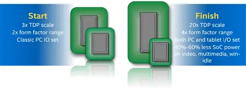
Skylake tries to address 4 major design goals: Scalability, Performance, Power, and Media & Graphics. Skylake started out as a "traditional client product" when initial design goals and development started back in 2010. At that time, Skylake was expected to cover products ranging from thin-and-lights all the way up to desktops. This translated to roughly 3x TDP scale and 2x form factor between the smallest and biggest models. With the introduction of Ultralight, Skylake design goals were extended to a new class of smaller form factors (down to 15 W). Skylake design goals were later further extended to more mobility segments and even smaller form factors. The final end result is a microarchitecture that now spans 20-fold TDP scale (from 3.5 W all the way to 80 W+) and up to 4-fold form factor between the lowest power model and the highest performance model. Intel claims that Skylake also succeeded in reducing power by 40-60% during important workloads such as video, graphics, and idle power which especially affect models where battery life is absolutely critical.
It's interesting to note that Skylake's end result managed to overlap and to some degree exceed Intel's own ultra-low power (ULP) series of microarchitectures (i.e. Silvermont and Goldmont).
Product Development Vectors:
- Form factor reduction - Emphasis was placed on reduction of form factor which includes both actual die size and package size.
- Platform minimization - Effort was spent on reducing the overall platform size include reduction of system board size, components, and power.
- Better life scenario power reduction - (mobile segment) The reduction of power during critical workloads such as video playback, video conferencing, and various other multimedia applications where the CPU itself is mostly idle.
- IA performance - Improvements to both power and performance of the CPU core
- IGP performance - Improvement to both power and performance of the GPU
- New Security technology - Better protection against hardware and software attacks
SoC design
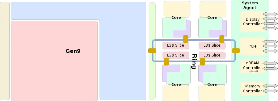
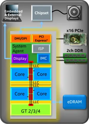
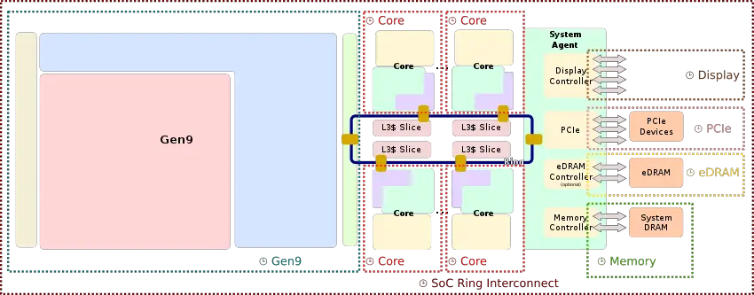
The Skylake system on a chip consists of a five major components: CPU core, LLC, Ring interconnect, System agent, and the integrated graphics. The image shown on the right, presented by Intel at the Intel Developer Forum in 2015, represents a hypothetical model incorporating all available features Skylake has to offer (i.e. superset of features). Skylake features an improved core (see § Pipeline) with higher performance per watt and higher performance per clock. The number of cores depends on the model, but mainstream mobile models are typically dual-core while mainstream desktop models are typically quad-core with dual-core desktop models still offered for value models (e.g. Celeron). Accompanying the cores is the LCC (last level cache or L3$ as seen from the CPU perspective). On mainstream parts the LLC consists of 2 MiB for each core with lower amounts for value models. Connecting the cores together is the ring interconnect. The ring extends to the GPU and the system agent as well. Intel further optimized the ring in Skylake for low-power and higher bandwidth.
Accompanying the cores is the Gen9 integrated graphics unit which comes in a number of different tiers ranging from just 12 execution units (used in the ultra-low power models) all the way the GT4 (Gen9 § Pipeline) with 72 execution units boasting a peak performance of up to 2,534.4 GFLOPS (HF) / 1,267.2 GFLOPS (SP) on the highest-end workstation model. The two highest-tier models are also accompanied by dedicated eDRAM ranging from 64 GiB to 120 GiB in capacity. The eDRAM is packaged along with the SoC in the same package.
On the other side is the System Agent (SA) which houses the various functionality that's not directly related to the cores or graphics. Skylake features an upgraded integrated memory controller (IMC) with most mainstream models supporting faster memory and dual-channel DDR4. The SA in Skylake also includes the Display Controller which now supports higher resolution displays with up to three displays for all mainstream models.
The SA also incorporates up to 20 lanes of PCIe with lesser amounts depending on the model. Of the 20 lanes, x16 PCIe lanes are offered for an external dedicated graphics hookup with the other four lanes reserved for communication with the southbridge chipset over Intel's new proprietary DMI 3.0 bus. The upgrade from DMI 2.0 (used in previous architectures) to 3.0 increased the bandwidth by 60% (8.0 GT/s from 5). For some models where form factor is exceptionally critical, such as those used for ultralight device, the chipset is packaged along with the SoC utilizing an on-package-interconnect (OPI) instead.
The last component of the System Agent and an entirely new addition in Skylake is the Image Processing Unit (IPU) which incorporates an image signal processor (ISP) on-die. The IPU is only available on mobile models and was added in order to improve and streamline (i.e. form factor and consistent set of features and quality) the implementation and performance of tablets and 2-in-1s. Previously this would require the assistance of an external component and the implementations varied by designer.
Core
Overview
Skylake shares most of the development vectors with its predecessor while introducing a one of new constraint. The overall goals were:
- Performance improvements - the traditional way of milking more performance by increasing the instructions per cycle as well as clock frequency.
- Power efficiency - reduction of power for all functional blocks
- Security enhancements - new security features are implemented in hardware in the core
- Configurability
Configurability
Intel has been experiencing a growing divergence in functionality over the last number of iterations of their microarchitecture between their mainstream consumer products and their high-end HPC/server models. Traditionally, Intel has been using the same exact core design for everything from their lowest end value models (e.g. Celeron) all the way up to the highest-performance enterprise models (e.g. Xeon E7). While the two have fundamentally different chip architectures, they use the same exact CPU core architecture as the building block.
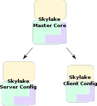
This design philosophy has changed with Skylake. In order to better accommodate the different functionalities of each segment without sacrificing features or making unnecessary compromises Intel went with a configurable core. The Skylake core is a single development project, making up a master superset core. The project result in two derivatives: one for servers and one for clients. All mainstream models (from Celeron/Pentium all the way up to Core i7/Xeon E3) use the client core configuration. Server models (e.g. Xeon E5/Xeon E7) will be using the new server configuration.
Pipeline
The Skylake core focuses on extracting performance and reducing power through a number of key ways. Intel builds Skylake on previous microarchitectures, descendants of Sandy Bridge. For the core to increase the overall performance, Intel focused on extracting additional parallelism.
Broad Overview
At a 5,000 foot view, Skylake represents the logical evolution from Haswell and Broadwell. Therefore, despite some significant differences from the previous microarchitecture, the overall designs is fundamentally the same and can be seen as enhancements over Broadwell rather than a complete change.
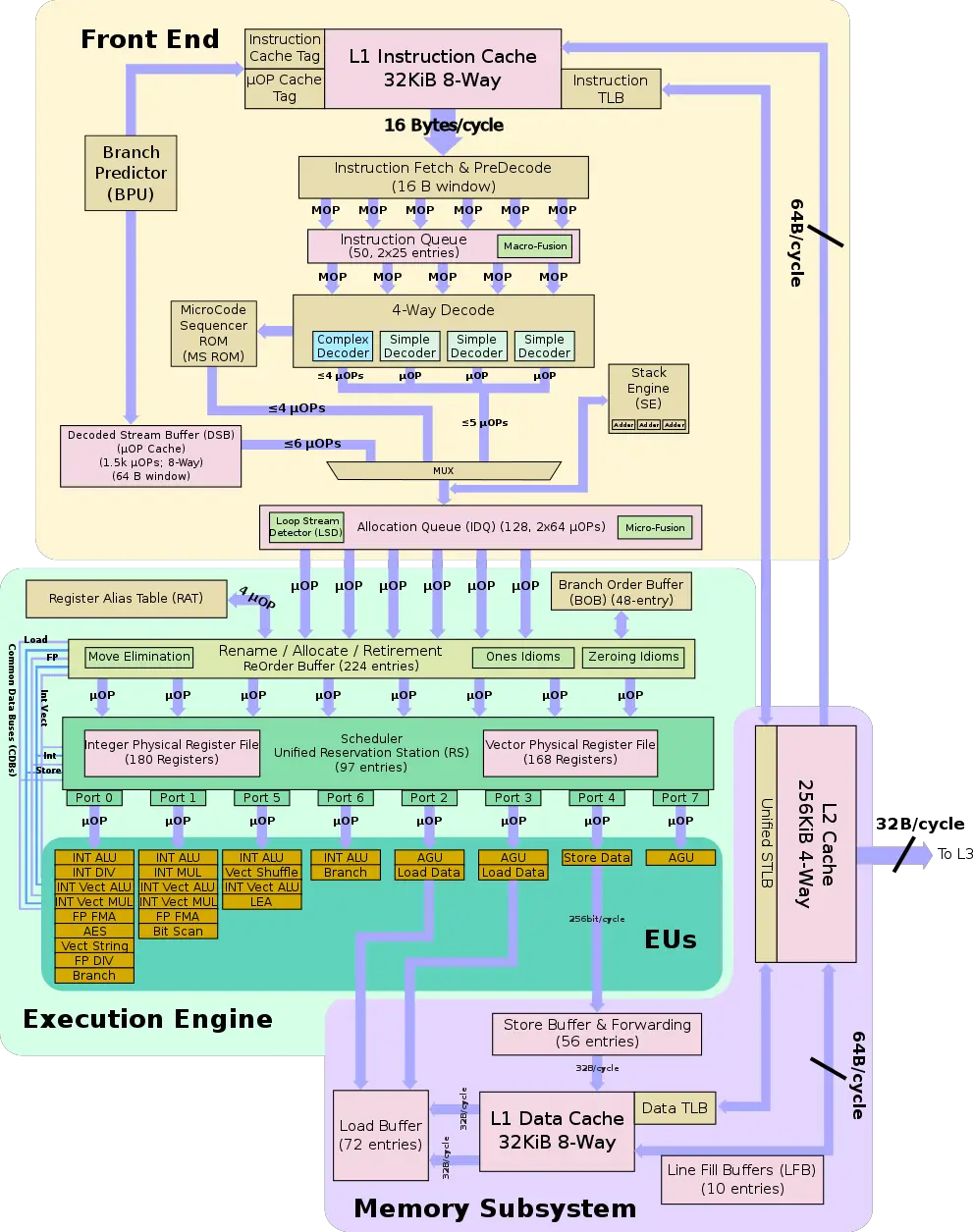
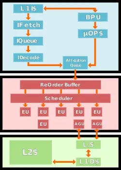
The pipeline can be broken down into three areas: the front-end, back-end or execution engine, and the memory subsystem. The goal of the front-end is to feed the back-end with a sufficient stream of operations which it gets by decoding instructions coming from memory. The front-end has two major pathways: the µOPs cache path and the legacy path. The legacy path is the traditional path whereby variable-length x86 instructions are fetched from the level 1 instruction cache, queued, and consequently get decoded into simpler, fixed-length µOPs. The alternative and much more desired path is the µOPs cache path whereby a cache containing already decoded µOPs receives a hit allowing the µOPs to be sent directly to the decode queue.
Regardless of which path an instruction ends up taking it will eventually arrive at the decode queue. The IDQ represents the end of the front-end and the in-order part of the machine and the start of the execution engine which operates out-of-order.
In the back-end, the micro-operations visit the reorder buffer. It's there where register allocation, renaming, and retiring takes place. At this stage a number of other optimizations are also done. From the reorder buffer, µOPs are sent to the unified scheduler. The scheduler has a number of exit ports, each wired to a set of different execution units. Some units can perform basic ALU operations, others can do multiplication and division, with some units capable of more complex operations such as various vector operations. The scheduler is effectively in charge of queuing the µOPs on the appropriate port so they can be executed by the appropriate unit.
Some µOPs deal with memory access (e.g. load & store). Those will be sent on dedicated scheduler ports that can perform those memory operations. Store operations go to the store buffer which is also capable of performing forwarding when needed. Likewise, Load operations come from the load buffer. Skylake features a dedicated 32 KiB level 1 data cache and a dedicated 32 KiB level 1 instruction cache. It also features a core-private 256 KiB L2 cache that is shared by both of the L1 caches.
Each core enjoys a slice of a third level of cache that is shared by all the core. In the client configuration for Skylake, there are either two cores or four cores connected while in the server configuration, up to 28 cores may be hooked together on a single chip.
Front-end
The front-end is is tasked with the challenge of fetching the complex x86 instructions from memory, decoding them, and delivering them to the execution units. In other words, the front end needs to be able to consistently deliver enough µOPs from the instruction code stream to keep the back-end busy. When the back-end is not being fully utilized, the core is not reaching its full performance. A poorly or under-performing front-end will translate directly to a poorly performing core. This challenge is further complicated by various redirection such as branches and the complex nature of the x86 instructions themselves.
Fetch & pre-decoding
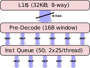
On their first pass, instructions should have already been prefetched from the L2 cache and into the L1 cache. The L1 is a 32 KiB, 8-way set associative cache, identical in size and organization to previous generations. Skylake fetching is done on a 16-byte fetch window. A window size that has not changed in a number of generations. Up to 16 bytes of code can be fetched each cycle. At this point they are still macro-ops (i.e. variable-length x86 architectural instruction). Instructions are brought into the pre-decode buffer for initial preparation.
x86 instructions are complex, variable length, have inconsistent encoding, and may contain multiple operations. At the pre-decode buffer the instructions boundaries get detected and marked. This is a fairly difficult task because each instruction can vary from a single byte all the way up to fifteen. Moreover, determining the length requires inspecting a couple of bytes of the instruction. In addition boundary marking, prefixes are also decoded and checked for various properties such as branches. As with previous microarchitectures, the pre-decoder has a throughput of 6 macro-ops per cycle or until all 16 bytes are consumed, whichever happens first. Note that the predecoder will not load a new 16-byte block until the previous block has been fully exhausted. For example, suppose a new chunk was loaded, resulting in 7 instructions. In the first cycle, 6 instructions will be processed and a whole second cycle will be wasted for that last instruction. This will produce the much lower throughput of 3.5 instructions per cycle which is considerably less than optimal. Likewise, if the 16-byte block resulted in just 4 instructions with 1 byte of the 5th instruction received, the first 4 instructions will be processed in the first cycle and a second cycle will be required for the last instruction. This will produce an average throughput of 2.5 instructions per cycle. Note that there is a special case for length-changing prefix (LCPs) which will incur additional pre-decoding costs. Real code is often less than 4 bytes which usually results in a good rate.
All of this works along with the branch prediction unit which attempts to guess the flow of instructions. In Skylake, the branch predictor has also been improved. The branch predictor now has reduced penalty (i.e. lower latency) for wrong direct jump target prediction. Additionally, the predictor in Skylake can inspect further in the byte stream than in previous architectures. The intimate improvements done in the branch predictor were not further disclosed by Intel.
Instruction Queue & MOP-Fusion
| MOP-Fusion Example: | ||
jne loop cmp eax, [mem] |
→ | cmpjne eax, [mem], loop |
The pre-decoded instructions are delivered to the Instruction Queue (IQ). In Broadwell, the Instruction Queue has been increased to 25 entries duplicated over for each thread (i.e. 50 total entries). It's unclear if that has changed with Skylake. One key optimization the instruction queue does is macro-op fusion. Skylake can fuse two macro-ops into a single complex one in a number of cases. In cases where a test or compare instruction with a subsequent conditional jump is detected, it will be converted into a single compare-and-branch instruction. Those fused instructions remain fused throughout the entire pipeline and get executed as a single operation by the branch unit thereby saving bandwidth everywhere.
Decoding
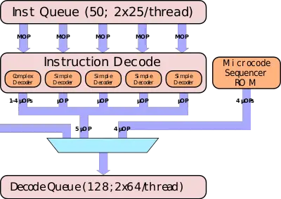
Up to five pre-decoded instructions are sent to the decoders each cycle. Decoders read in macro-operations and emit regular, fixed length µOPs. Skylake represents a big genealogical change from the last couple of microarchitectures. Skylake's pipeline is wider than it predecessors; Skylake adds another simple decoder. The five decoders are asymmetric; the first one, Decoder 0, is a complex decoder while the other four are simple decoders. A simple decoder is capable of translating instructions that emit a single fused-µOP. By contrast, a complex decoder can decode anywhere from one to four fused-µOPs. Skylake is now capable of decoding 5 macro-ops per cycle or 25% more than Broadwell, however this does not translates directly to direct IPC uplift to due to various other more restricting points in the pipeline. Intel chose not increase the number of complex decoders because much harder to extract additional parallelism from that. Overall up to 5 simple instructions or 1 complex x86 instruction may be decoded each cycle.
MSROM & Stack Engine
There are more complex instructions that are not trivial to be decoded even by complex decoder. For instructions that transform into more than four µOPs, the instruction detours through the microcode sequencer (MS) ROM. When that happens, up to 4 µOPs/cycle are emitted until the microcode sequencer is done. During that time, the decoders are disabled.
x86 has dedicated stack machine operations. Instructions such as PUSH, POP, as well as CALL, and RET all operate on the stack pointer (ESP). Without any specialized hardware, such operations would would need to be sent to the back-end for execution using the general purpose ALUs, using up some of the bandwidth and utilizing scheduler and execution units resources. Since Pentium M, Intel has been making use of a Stack Engine. The Stack Engine has a set of three dedicated adders it uses to perform and eliminate the stack-updating µOPs (i.e. capable of handling three additions per cycle). Instruction such as PUSH are translated into a store and a subtraction of 4 from ESP. The subtraction in this case will be done by the Stack Engine. The Stack Engine sits after the decoders and monitors the µOPs stream as it passes by. Incoming stack-modifying operations are caught by the Stack Engine. This operation alleviate the burden of the pipeline from stack pointer-modifying µOPs. In other words, it's cheaper and faster to calculate stack pointer targets at the Stack Engine than it is to send those operations down the pipeline to be done by the execution units (i.e., general purpose ALUs).
µOP cache & x86 tax
Decoding the variable-length, inconsistent, and complex x86 instructions is a nontrivial task. It's also expensive in terms of performance and power. Therefore, the best way for the pipeline to avoid those things is to simply not decode the instructions. This is the job of the µOP cache or the Decoded Stream Buffer (DSB). Skylake's µOP cache is organized similarly to previous generations like Sandy Bridge, however both the bandwidth and the tracking window was increased. The cache is organized into 32 sets of 8 cache lines with each line holding up to 6 µOP for a total of 1,536 µOPs. Whereas previously (e.g. Haswell) the µOP cache operated on 32-byte windows, in Skylake the window size has been doubled to 64-bytes. The micro-operation cache is competitively shared between the two threads and can also hold pointers to the microcode.
A hit in the µOP allows for up to 6 µOP (i.e., entire line) per cycle to be sent directly to the Instruction Decode Queue (IDQ), bypassing all the pre-decoding and decoding that would otherwise have to be done. Whereas the legacy decode path works in 16-byte instruction fetch windows, the µOP cache has no such restriction and can deliver 6 µOP/cycle corresponding to the much bigger 64-byte window. Previously (e.g., Broadwell), the bandwidth was lower at 4 µOP per cycle. The 1.5x bandwidth increase greatly improves the numbers of µOP that the back-end can take advantage of in the out-of-order part of the machine.
Allocation Queue & µOP-Fusion
The emitted µOPs from the decoders are sent directly to the Allocation Queue (AQ) or Instruction Decode Queue (IDQ). The Allocation Queue acts as the interface between the front-end (in-order) and the back-end (out-of-order). Skylake's Allocation Queue is quadrupled from Broadwell from 28-entries per thread to 64-entries per thread.
Execution engine
Like the front-end, the execution engine's ReOrder buffer has been increased to 224 entries (from 192 in Broadwell) in order to extract more instruction-level parallelism. Likewise the scheduler itself was increased considerably to 97 entries (from 64 in Broadwell). The integer register file was also slightly increased from 160 entries to 180.
The scheduler had its ports rearranged to better balance various instructions. For example, divide and sqrt instructions latency and throughput were improved. The latency and throughput of floating point ADD, MUL, and FMA were made uniformed at 4 cycles with a throughput of 2 ops/clock. Likewise the latency of AES instructions were significantly reduced from 7 cycles down to 4.
| Dispatch Ports | |||||||
|---|---|---|---|---|---|---|---|
| Port 0 | Port 1 | Port 2 | Port 3 | Port 4 | Port 5 | Port 6 | Port 7 |
| ALU Vec ALU |
ALU Fast LEA Vec ALU |
Load Addr Store Addr |
Load Addr Store Addr |
Store Data | ALU Fast LEA Vec ALU |
ALU Shift |
Store Addr |
| Vec Shift Vec Add |
Vec Shift Vec Add |
Vec Shuffle | Branch | ||||
| Vec Mul FMA |
Vec Mul FMA |
||||||
| DIV | Slow Int | ||||||
| Branch2 | Slow LEA | ||||||
Execution Units
| Execution Units | ||
|---|---|---|
| Execution Unit | # of Units | Instructions |
| ALU | 4 | add, and, cmp, or, test, xor, movzx, movsx, mov, (v)movdqu, (v)movdqa, (v)movap*, (v)movup* |
| DIV | 1 | divp*, divs*, vdiv*, sqrt*, vsqrt*, rcp*, vrcp*, rsqrt*, idiv |
| Shift | 2 | sal, shl, rol, adc, sarx, adcx, adox, etc... |
| Shuffle | 1 | (v)shufp*, vperm*, (v)pack*, (v)unpck*, (v)punpck*, (v)pshuf*, (v)pslldq, (v)alignr, (v)pmovzx*, vbroadcast*, (v)pslldq, (v)psrldq, (v)pblendw |
| Slow Int | 1 | mul, imul, bsr, rcl, shld, mulx, pdep, etc... |
| BM Bit Manipulation |
2 | andn, bextr, blsi, blsmsk, bzhi, etc |
| FP Mov | 1 | (v)movsd/ss, (v)movd gpr |
| SIMD Misc | 1 | STTNI, (v)pclmulqdq, (v)psadw, vector shift count in xmm |
| Vec ALU | 3 | (v)pand, (v)por, (v)pxor, (v)movq, (v)movq, (v)movap*, (v)movup*, (v)andp*, (v)orp*, (v)paddb/w/d/q, (v)blendv*, (v)blendp*, (v)pblendd |
| Vec Shift | 2 | (v)psllv*, (v)psrlv*, vector shift count in imm8 |
| Vec Add | 2 | (v)addp*, (v)cmpp*, (v)max*, (v)min*, (v)padds*, (v)paddus*, (v)psign, (v)pabs, (v)pavgb, (v)pcmpeq*, (v)pmax, (v)cvtps2dq, (v)cvtdq2ps, (v)cvtsd2si, (v)cvtss2si |
| Vec Mul | 2 | (v)mul*, (v)pmul*, (v)pmadd* |
Memory subsystem
Skylake has had its store buffer enlarged to 56 entries (up from 42 in Broadwell). Special care was taken to reduce the penalty for page-split loads: previously scenarios involving page-split loads were thought to be rarer than they actually are. This was addressed in Skylake with page-split loads are now made equal to other splits loads. Expect page split load penalty down to 5 cycles from 100 cycles in Broadwell. The average latency to forward a load to store has also been improved and stores that miss in the L1$ generate L2$ requests to the next level cache much earlier in Sklake than before.
The bandwidth from L2$ to L3$ has been improved and write bandwidth from L2$ to L3$ has also been increased from 4 cycles/line to 2 cycles/line.
eDRAM architectural changes
Intel ships a number of products with Embedded DRAM incorporated on package in order to increase performance of the integrated graphics and to a lesser degree the code through additional bandwidth and caching. There has been a number of significant architectural changes in how the eDRAM works in Skylake.
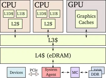
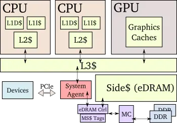
In Broadwell, the eDRAM was statically attached to the LLC (last level cache, L3$ from the perspective of the CPU Cores and L4$ from the perspective of the IGP), effectively stealing half a Mebibyte per core in the process, but behaving as an architectural true level 4 cache. This was fundamentally changed in Skylake. In Skylake, Intel removed the eDRAM from the LLC to its own array, re-freeing the 512 KiB (hence the 1.5 MiB/core in Broadwell and 2 MiB back in Skylake), but also removing the undesired dependency between the capacity of the eDRAM and the number of cores. Skylake's cache is effectively no longer a true level 4 cache but rather a memory side cache. This has a number of benefits such as that each and every memory access that goes through the memory controller gets looked up in the eDRAM. On a satisfied hit, the value is obtained from there. On a miss, a value gets allocated and stored in the eDRAM (subject to a number of restrictions, for example no I/O devices requests get cached on the eDRAM).
| Skylake vs Broadwell eDRAM Architecture | |
|---|---|
| Broadwell | Skylake |
 |
|
The new eDRAM changes mean it's no longer architectural - capable of caching any data (including "unreachable memory", display engines, and effectively any memory transfer not bound by software restrictions) and is entirely invisible to software (one exception noted later) in terms of coherency (note that no flushing is thus necessary to maintain coherency), ordering, or other organizational details. For optimal graphics performance, the graphics driver may decide to limit certain memory accesses to only the eDRAM, only the LLC, or in both of them.
Clock domains
Skylake is divided into a number of clock domains, each controlling the clock frequency of their respective unit in the processor. All clock domains are some multiple of the [virtual] bus clock (BCLK).
- BCLK - Bus Clock - The system bus interface frequency (once upon a time referred to the actual FSB speed, it now serves as only a base clock reference for all other clock domains). The bus clock is 100 MHz.
- Core Clock - The frequency at which the core and the L1/L2 caches operate at. (Frequency depends on the model and is represented as a multiple of BCLK).
- Ring Clock - The frequency at which the ring interconnect and LLC operate at. Data from/to the individual cores are read/written into the L3 at a rate of 32B/cycle operating at Ring Clock frequency.
- IGP Clock - The frequency at which the integrated graphics (Gen9 GPU) operates at. Data from/to the GPU are read/written into the LLC at a rate of 64B/cycle operating at this frequency as well.
- eDRAM Clock - The frequency at which the embedded DRAM operates at (only available for certain models). Data is read/written from/to the LLC at a rate of 32B/cycle operating at this frequency as well.
- MemClk - Memory Clock - The frequency at which the system DRAM operates at. DRAM data is transfered at a rate of 8B/cycle operating at MemClk frequency.
Die
Client Die
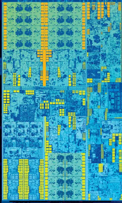
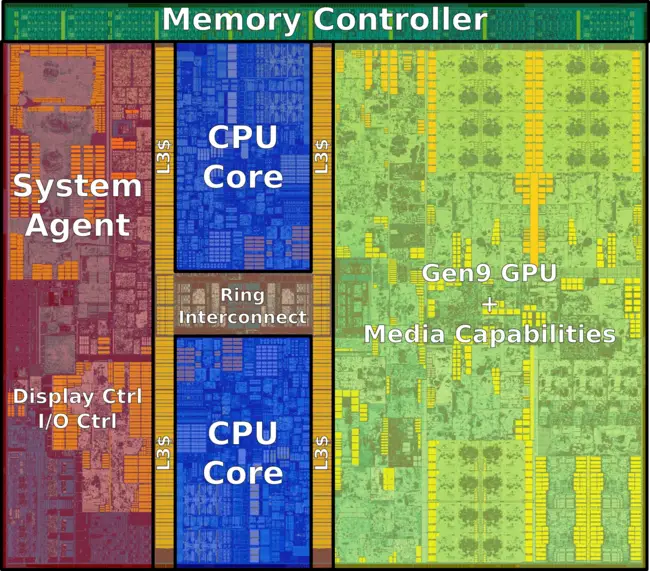
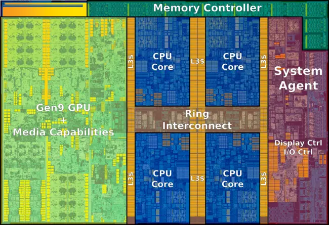
Skylake desktop and mobile come and 2 and 4 cores. Each variant has its own die. One of the most noticeable changes on die is the amount of die space allocated to the GPU. The major components of the die is:
- System Agent
- CPU Core
- Ring bus interconnect
- Memory Controller
System Agent
The System Agent (SA) contains the Image Processing Unit (IPU), the Display Engine (DE), the I/O bus and various other shared functionality. Note that the mainstream desktop (i.e., quad-core die) does not have an IPU (The memory controller actually occupies a portion of where it would otherwise be).
Integrated Graphics
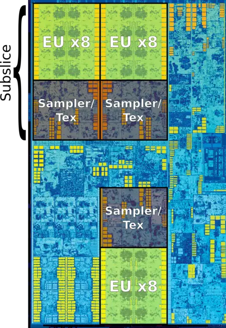
The integrated graphics takes up the largest portion of the die. The normal dual-core and quad-core dies come with 24 EU Gen9.5 GPU (with 12 units disabled on the low end models).
Dual-core
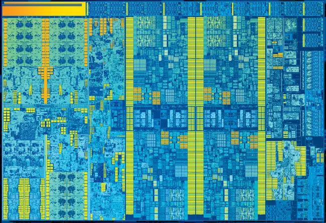
Die shot of the dual-core Skylake processors. Those are found in mobile models, and entry-level/budget processors:
- 14 nm process
- 11 metal layers
- ~1,750,000,000 transistors
- ~95.33 mm²
Quad-core
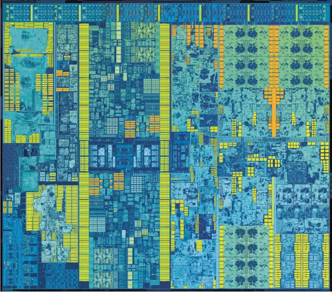
Die shot of the quad-core Skyllake processors. Those are found in almost all mainstream desktop processors.
- 14 nm process
- 11 metal layers
- ~122 mm²
Server Die
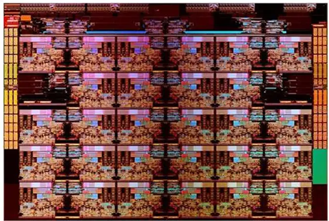
Skylake Server class models consist of 3 different dies: Low Core Count (LCC), Medium Core Count (MCC), and High Core Count (HCC).
High Core Count (HCC)
Added instructions
SGX - Software Guard Extensions
| Full list |
|---|
MPX - Memory Protection Extensions
| Full list |
|---|
AVX-512 - Advanced Vector Extensions 512; These instructions can only be found on selected high-end Xeon models (codename SKX)
Cores
| This section is empty; you can help add the missing info by editing this page. |
All Skylake Chips
| Skylake Chips | |||||||||||
|---|---|---|---|---|---|---|---|---|---|---|---|
| Main processor | IGP | ||||||||||
| Model | µarch | Platform | Core | Launched | SDP | TDP | Freq | Max Mem | Name | Freq | Max Freq |
| 3855U | Skylake | Skylake U | 27 December 2015 | 15 W 15,000 mW 0.0201 hp 0.015 kW | 1.6 GHz 1,600 MHz 1,600,000 kHz | 32,768 MiB 33,554,432 KiB 34,359,738,368 B 32 GiB 0.0313 TiB | HD Graphics 510 | 300 MHz 0.3 GHz 300,000 KHz | 900 MHz 0.9 GHz 900,000 KHz | ||
| 3955U | Skylake | Skylake U | 27 December 2015 | 15 W 15,000 mW 0.0201 hp 0.015 kW | 2 GHz 2,000 MHz 2,000,000 kHz | 32,768 MiB 33,554,432 KiB 34,359,738,368 B 32 GiB 0.0313 TiB | HD Graphics 510 | 300 MHz 0.3 GHz 300,000 KHz | 900 MHz 0.9 GHz 900,000 KHz | ||
| G3900 | Skylake | Skylake S | 19 October 2015 | 51 W 51,000 mW 0.0684 hp 0.051 kW | 2.8 GHz 2,800 MHz 2,800,000 kHz | 65,536 MiB 67,108,864 KiB 68,719,476,736 B 64 GiB 0.0625 TiB | HD Graphics 510 | 350 MHz 0.35 GHz 350,000 KHz | 950 MHz 0.95 GHz 950,000 KHz | ||
| G3900E | Skylake | Skylake H | 2 January 2016 | 35 W 35,000 mW 0.0469 hp 0.035 kW | 2.4 GHz 2,400 MHz 2,400,000 kHz | 65,536 MiB 67,108,864 KiB 68,719,476,736 B 64 GiB 0.0625 TiB | HD Graphics 510 | 350 MHz 0.35 GHz 350,000 KHz | 950 MHz 0.95 GHz 950,000 KHz | ||
| G3900T | Skylake | Skylake S | 19 October 2015 | 35 W 35,000 mW 0.0469 hp 0.035 kW | 2.6 GHz 2,600 MHz 2,600,000 kHz | 65,536 MiB 67,108,864 KiB 68,719,476,736 B 64 GiB 0.0625 TiB | HD Graphics 510 | 350 MHz 0.35 GHz 350,000 KHz | 950 MHz 0.95 GHz 950,000 KHz | ||
| G3900TE | Skylake | Skylake S | 19 October 2015 | 35 W 35,000 mW 0.0469 hp 0.035 kW | 2.3 GHz 2,300 MHz 2,300,000 kHz | 65,536 MiB 67,108,864 KiB 68,719,476,736 B 64 GiB 0.0625 TiB | HD Graphics 510 | 350 MHz 0.35 GHz 350,000 KHz | 950 MHz 0.95 GHz 950,000 KHz | ||
| G3902E | Skylake | Skylake H | 2 January 2016 | 25 W 25,000 mW 0.0335 hp 0.025 kW | 1.6 GHz 1,600 MHz 1,600,000 kHz | 65,536 MiB 67,108,864 KiB 68,719,476,736 B 64 GiB 0.0625 TiB | HD Graphics 510 | 350 MHz 0.35 GHz 350,000 KHz | 950 MHz 0.95 GHz 950,000 KHz | ||
| G3920 | Skylake | Skylake S | 19 October 2015 | 51 W 51,000 mW 0.0684 hp 0.051 kW | 2.9 GHz 2,900 MHz 2,900,000 kHz | 65,536 MiB 67,108,864 KiB 68,719,476,736 B 64 GiB 0.0625 TiB | HD Graphics 510 | 350 MHz 0.35 GHz 350,000 KHz | 950 MHz 0.95 GHz 950,000 KHz | ||
| i3-6006U | Skylake | Skylake U | 10 November 2016 | 15 W 15,000 mW 0.0201 hp 0.015 kW | 2 GHz 2,000 MHz 2,000,000 kHz | 32,768 MiB 33,554,432 KiB 34,359,738,368 B 32 GiB 0.0313 TiB | HD Graphics 520 | 300 MHz 0.3 GHz 300,000 KHz | 900 MHz 0.9 GHz 900,000 KHz | ||
| i3-6098P | Skylake | Skylake S | 27 December 2015 | 54 W 54,000 mW 0.0724 hp 0.054 kW | 3.6 GHz 3,600 MHz 3,600,000 kHz | 65,536 MiB 67,108,864 KiB 68,719,476,736 B 64 GiB 0.0625 TiB | HD Graphics 510 | 350 MHz 0.35 GHz 350,000 KHz | 1,050 MHz 1.05 GHz 1,050,000 KHz | ||
| i3-6100 | Skylake | Skylake S | 27 September 2015 | 51 W 51,000 mW 0.0684 hp 0.051 kW | 3.7 GHz 3,700 MHz 3,700,000 kHz | 65,536 MiB 67,108,864 KiB 68,719,476,736 B 64 GiB 0.0625 TiB | HD Graphics 530 | 350 MHz 0.35 GHz 350,000 KHz | 1,050 MHz 1.05 GHz 1,050,000 KHz | ||
| i3-6100E | Skylake | Skylake H | 12 October 2015 | 35 W 35,000 mW 0.0469 hp 0.035 kW | 2.7 GHz 2,700 MHz 2,700,000 kHz | 65,536 MiB 67,108,864 KiB 68,719,476,736 B 64 GiB 0.0625 TiB | HD Graphics 530 | 350 MHz 0.35 GHz 350,000 KHz | 950 MHz 0.95 GHz 950,000 KHz | ||
| i3-6100H | Skylake | Skylake H | 27 September 2015 | 35 W 35,000 mW 0.0469 hp 0.035 kW | 2.7 GHz 2,700 MHz 2,700,000 kHz | 65,536 MiB 67,108,864 KiB 68,719,476,736 B 64 GiB 0.0625 TiB | HD Graphics 530 | 350 MHz 0.35 GHz 350,000 KHz | 900 MHz 0.9 GHz 900,000 KHz | ||
| i3-6100T | Skylake | Skylake S | 27 September 2015 | 35 W 35,000 mW 0.0469 hp 0.035 kW | 3.2 GHz 3,200 MHz 3,200,000 kHz | 65,536 MiB 67,108,864 KiB 68,719,476,736 B 64 GiB 0.0625 TiB | HD Graphics 530 | 350 MHz 0.35 GHz 350,000 KHz | 950 MHz 0.95 GHz 950,000 KHz | ||
| i3-6100TE | Skylake | Skylake S | 12 October 2015 | 35 W 35,000 mW 0.0469 hp 0.035 kW | 2.7 GHz 2,700 MHz 2,700,000 kHz | 65,536 MiB 67,108,864 KiB 68,719,476,736 B 64 GiB 0.0625 TiB | HD Graphics 530 | 350 MHz 0.35 GHz 350,000 KHz | 1,000 MHz 1 GHz 1,000,000 KHz | ||
| i3-6100U | Skylake | Skylake U | 27 September 2015 | 15 W 15,000 mW 0.0201 hp 0.015 kW | 2.3 GHz 2,300 MHz 2,300,000 kHz | 32,768 MiB 33,554,432 KiB 34,359,738,368 B 32 GiB 0.0313 TiB | HD Graphics 520 | 300 MHz 0.3 GHz 300,000 KHz | 1,000 MHz 1 GHz 1,000,000 KHz | ||
| i3-6102E | Skylake | Skylake H | 12 October 2015 | 25 W 25,000 mW 0.0335 hp 0.025 kW | 1.9 GHz 1,900 MHz 1,900,000 kHz | 65,536 MiB 67,108,864 KiB 68,719,476,736 B 64 GiB 0.0625 TiB | HD Graphics 530 | 350 MHz 0.35 GHz 350,000 KHz | 950 MHz 0.95 GHz 950,000 KHz | ||
| i3-6120T | Skylake | Skylake S | 35 W 35,000 mW 0.0469 hp 0.035 kW | 65,536 MiB 67,108,864 KiB 68,719,476,736 B 64 GiB 0.0625 TiB | HD Graphics 530 | 350 MHz 0.35 GHz 350,000 KHz | 950 MHz 0.95 GHz 950,000 KHz | ||||
| i3-6157U | Skylake | Skylake U | June 2016 | 28 W 28,000 mW 0.0375 hp 0.028 kW | 2.4 GHz 2,400 MHz 2,400,000 kHz | 32,768 MiB 33,554,432 KiB 34,359,738,368 B 32 GiB 0.0313 TiB | Iris Graphics 550 | 300 MHz 0.3 GHz 300,000 KHz | 1,000 MHz 1 GHz 1,000,000 KHz | ||
| i3-6167U | Skylake | Skylake U | 27 September 2015 | 28 W 28,000 mW 0.0375 hp 0.028 kW | 2.7 GHz 2,700 MHz 2,700,000 kHz | 32,768 MiB 33,554,432 KiB 34,359,738,368 B 32 GiB 0.0313 TiB | Iris Graphics 550 | 300 MHz 0.3 GHz 300,000 KHz | 1,000 MHz 1 GHz 1,000,000 KHz | ||
| i3-6300 | Skylake | Skylake S | 27 September 2015 | 51 W 51,000 mW 0.0684 hp 0.051 kW | 3.8 GHz 3,800 MHz 3,800,000 kHz | 65,536 MiB 67,108,864 KiB 68,719,476,736 B 64 GiB 0.0625 TiB | HD Graphics 530 | 350 MHz 0.35 GHz 350,000 KHz | 1,150 MHz 1.15 GHz 1,150,000 KHz | ||
| i3-6300T | Skylake | Skylake S | 27 September 2015 | 35 W 35,000 mW 0.0469 hp 0.035 kW | 3.3 GHz 3,300 MHz 3,300,000 kHz | 65,536 MiB 67,108,864 KiB 68,719,476,736 B 64 GiB 0.0625 TiB | HD Graphics 530 | 350 MHz 0.35 GHz 350,000 KHz | 950 MHz 0.95 GHz 950,000 KHz | ||
| i3-6320 | Skylake | Skylake S | 27 September 2015 | 51 W 51,000 mW 0.0684 hp 0.051 kW | 3.9 GHz 3,900 MHz 3,900,000 kHz | 65,536 MiB 67,108,864 KiB 68,719,476,736 B 64 GiB 0.0625 TiB | HD Graphics 530 | 350 MHz 0.35 GHz 350,000 KHz | 1,150 MHz 1.15 GHz 1,150,000 KHz | ||
| i3-6320T | Skylake | Skylake S | 35 W 35,000 mW 0.0469 hp 0.035 kW | 65,536 MiB 67,108,864 KiB 68,719,476,736 B 64 GiB 0.0625 TiB | HD Graphics 530 | 350 MHz 0.35 GHz 350,000 KHz | 950 MHz 0.95 GHz 950,000 KHz | ||||
| i5-6198DU | Skylake | Skylake U | 27 December 2015 | 15 W 15,000 mW 0.0201 hp 0.015 kW | 2.3 GHz 2,300 MHz 2,300,000 kHz | 32,768 MiB 33,554,432 KiB 34,359,738,368 B 32 GiB 0.0313 TiB | HD Graphics 510 | 300 MHz 0.3 GHz 300,000 KHz | 1,000 MHz 1 GHz 1,000,000 KHz | ||
| i5-6200U | Skylake | Skylake U | 27 September 2015 | 15 W 15,000 mW 0.0201 hp 0.015 kW | 2.3 GHz 2,300 MHz 2,300,000 kHz | 32,768 MiB 33,554,432 KiB 34,359,738,368 B 32 GiB 0.0313 TiB | HD Graphics 520 | 300 MHz 0.3 GHz 300,000 KHz | 1,000 MHz 1 GHz 1,000,000 KHz | ||
| i5-6260U | Skylake | Skylake U | 27 September 2015 | 15 W 15,000 mW 0.0201 hp 0.015 kW | 1.8 GHz 1,800 MHz 1,800,000 kHz | 32,768 MiB 33,554,432 KiB 34,359,738,368 B 32 GiB 0.0313 TiB | Iris Graphics 540 | 300 MHz 0.3 GHz 300,000 KHz | 950 MHz 0.95 GHz 950,000 KHz | ||
| i5-6267U | Skylake | Skylake U | 27 September 2015 | 28 W 28,000 mW 0.0375 hp 0.028 kW | 2.9 GHz 2,900 MHz 2,900,000 kHz | 32,768 MiB 33,554,432 KiB 34,359,738,368 B 32 GiB 0.0313 TiB | Iris Graphics 550 | 300 MHz 0.3 GHz 300,000 KHz | 1,050 MHz 1.05 GHz 1,050,000 KHz | ||
| i5-6287U | Skylake | Skylake U | 27 September 2015 | 28 W 28,000 mW 0.0375 hp 0.028 kW | 3.1 GHz 3,100 MHz 3,100,000 kHz | 32,768 MiB 33,554,432 KiB 34,359,738,368 B 32 GiB 0.0313 TiB | Iris Graphics 550 | 300 MHz 0.3 GHz 300,000 KHz | 1,100 MHz 1.1 GHz 1,100,000 KHz | ||
| i5-6300HQ | Skylake | Skylake H | 27 September 2015 | 45 W 45,000 mW 0.0603 hp 0.045 kW | 2.3 GHz 2,300 MHz 2,300,000 kHz | 65,536 MiB 67,108,864 KiB 68,719,476,736 B 64 GiB 0.0625 TiB | HD Graphics 530 | 350 MHz 0.35 GHz 350,000 KHz | 950 MHz 0.95 GHz 950,000 KHz | ||
| i5-6300U | Skylake | Skylake U | 27 September 2015 | 15 W 15,000 mW 0.0201 hp 0.015 kW | 2.4 GHz 2,400 MHz 2,400,000 kHz | 32,768 MiB 33,554,432 KiB 34,359,738,368 B 32 GiB 0.0313 TiB | HD Graphics 520 | 300 MHz 0.3 GHz 300,000 KHz | 1,000 MHz 1 GHz 1,000,000 KHz | ||
| i5-6350HQ | Skylake | Skylake H | 2 January 2016 | 45 W 45,000 mW 0.0603 hp 0.045 kW | 2.3 GHz 2,300 MHz 2,300,000 kHz | 65,536 MiB 67,108,864 KiB 68,719,476,736 B 64 GiB 0.0625 TiB | Iris Pro Graphics 580 | 350 MHz 0.35 GHz 350,000 KHz | 900 MHz 0.9 GHz 900,000 KHz | ||
| i5-6360U | Skylake | Skylake U | 27 September 2015 | 15 W 15,000 mW 0.0201 hp 0.015 kW | 2 GHz 2,000 MHz 2,000,000 kHz | 32,768 MiB 33,554,432 KiB 34,359,738,368 B 32 GiB 0.0313 TiB | Iris Graphics 540 | 300 MHz 0.3 GHz 300,000 KHz | 1,000 MHz 1 GHz 1,000,000 KHz | ||
| i5-6400 | Skylake | Skylake S | 27 September 2015 | 65 W 65,000 mW 0.0872 hp 0.065 kW | 2.7 GHz 2,700 MHz 2,700,000 kHz | 65,536 MiB 67,108,864 KiB 68,719,476,736 B 64 GiB 0.0625 TiB | HD Graphics 530 | 350 MHz 0.35 GHz 350,000 KHz | 950 MHz 0.95 GHz 950,000 KHz | ||
| i5-6400T | Skylake | Skylake S | 27 September 2015 | 35 W 35,000 mW 0.0469 hp 0.035 kW | 2.2 GHz 2,200 MHz 2,200,000 kHz | 65,536 MiB 67,108,864 KiB 68,719,476,736 B 64 GiB 0.0625 TiB | HD Graphics 530 | 350 MHz 0.35 GHz 350,000 KHz | 950 MHz 0.95 GHz 950,000 KHz | ||
| i5-6402P | Skylake | Skylake S | 27 December 2015 | 65 W 65,000 mW 0.0872 hp 0.065 kW | 2.8 GHz 2,800 MHz 2,800,000 kHz | 65,536 MiB 67,108,864 KiB 68,719,476,736 B 64 GiB 0.0625 TiB | HD Graphics 510 | 350 MHz 0.35 GHz 350,000 KHz | 950 MHz 0.95 GHz 950,000 KHz | ||
| i5-6440EQ | Skylake | Skylake H | 12 October 2015 | 45 W 45,000 mW 0.0603 hp 0.045 kW | 2.7 GHz 2,700 MHz 2,700,000 kHz | 65,536 MiB 67,108,864 KiB 68,719,476,736 B 64 GiB 0.0625 TiB | HD Graphics 530 | 350 MHz 0.35 GHz 350,000 KHz | 1,000 MHz 1 GHz 1,000,000 KHz | ||
| i5-6440HQ | Skylake | Skylake H | 27 October 2015 | 45 W 45,000 mW 0.0603 hp 0.045 kW | 2.6 GHz 2,600 MHz 2,600,000 kHz | 65,536 MiB 67,108,864 KiB 68,719,476,736 B 64 GiB 0.0625 TiB | HD Graphics 530 | 350 MHz 0.35 GHz 350,000 KHz | 950 MHz 0.95 GHz 950,000 KHz | ||
| i5-6442EQ | Skylake | Skylake H | 12 October 2015 | 25 W 25,000 mW 0.0335 hp 0.025 kW | 1.9 GHz 1,900 MHz 1,900,000 kHz | 65,536 MiB 67,108,864 KiB 68,719,476,736 B 64 GiB 0.0625 TiB | HD Graphics 530 | 350 MHz 0.35 GHz 350,000 KHz | 1,000 MHz 1 GHz 1,000,000 KHz | ||
| i5-6500 | Skylake | Skylake S | 27 September 2015 | 65 W 65,000 mW 0.0872 hp 0.065 kW | 3.2 GHz 3,200 MHz 3,200,000 kHz | 65,536 MiB 67,108,864 KiB 68,719,476,736 B 64 GiB 0.0625 TiB | HD Graphics 530 | 350 MHz 0.35 GHz 350,000 KHz | 1,050 MHz 1.05 GHz 1,050,000 KHz | ||
| i5-6500T | Skylake | Skylake S | 27 September 2015 | 35 W 35,000 mW 0.0469 hp 0.035 kW | 2.5 GHz 2,500 MHz 2,500,000 kHz | 65,536 MiB 67,108,864 KiB 68,719,476,736 B 64 GiB 0.0625 TiB | HD Graphics 530 | 350 MHz 0.35 GHz 350,000 KHz | 1,100 MHz 1.1 GHz 1,100,000 KHz | ||
| i5-6500TE | Skylake | Skylake S | 19 October 2015 | 35 W 35,000 mW 0.0469 hp 0.035 kW | 2.3 GHz 2,300 MHz 2,300,000 kHz | 65,536 MiB 67,108,864 KiB 68,719,476,736 B 64 GiB 0.0625 TiB | HD Graphics 530 | 350 MHz 0.35 GHz 350,000 KHz | 1,000 MHz 1 GHz 1,000,000 KHz | ||
| i5-6585R | Skylake | Skylake H | 22 April 2016 | 65 W 65,000 mW 0.0872 hp 0.065 kW | 2.8 GHz 2,800 MHz 2,800,000 kHz | 65,536 MiB 67,108,864 KiB 68,719,476,736 B 64 GiB 0.0625 TiB | Iris Pro Graphics 580 | 350 MHz 0.35 GHz 350,000 KHz | 1,100 MHz 1.1 GHz 1,100,000 KHz | ||
| i5-6600 | Skylake | Skylake S | 27 September 2015 | 65 W 65,000 mW 0.0872 hp 0.065 kW | 3.3 GHz 3,300 MHz 3,300,000 kHz | 65,536 MiB 67,108,864 KiB 68,719,476,736 B 64 GiB 0.0625 TiB | HD Graphics 530 | 350 MHz 0.35 GHz 350,000 KHz | 1,150 MHz 1.15 GHz 1,150,000 KHz | ||
| i5-6600K | Skylake | Skylake S | 27 September 2015 | 91 W 91,000 mW 0.122 hp 0.091 kW | 3.5 GHz 3,500 MHz 3,500,000 kHz | 65,536 MiB 67,108,864 KiB 68,719,476,736 B 64 GiB 0.0625 TiB | HD Graphics 530 | 350 MHz 0.35 GHz 350,000 KHz | 1,150 MHz 1.15 GHz 1,150,000 KHz | ||
| i5-6600T | Skylake | Skylake S | 27 September 2015 | 35 W 35,000 mW 0.0469 hp 0.035 kW | 2.7 GHz 2,700 MHz 2,700,000 kHz | 65,536 MiB 67,108,864 KiB 68,719,476,736 B 64 GiB 0.0625 TiB | HD Graphics 530 | 350 MHz 0.35 GHz 350,000 KHz | 1,100 MHz 1.1 GHz 1,100,000 KHz | ||
| i5-6685R | Skylake | Skylake H | 22 April 2016 | 65 W 65,000 mW 0.0872 hp 0.065 kW | 3.2 GHz 3,200 MHz 3,200,000 kHz | 65,536 MiB 67,108,864 KiB 68,719,476,736 B 64 GiB 0.0625 TiB | Iris Pro Graphics 580 | 350 MHz 0.35 GHz 350,000 KHz | 1,150 MHz 1.15 GHz 1,150,000 KHz | ||
| i7-10510U | Skylake | Comet Lake | 15 W 15,000 mW 0.0201 hp 0.015 kW | 1.8 GHz 1,800 MHz 1,800,000 kHz | |||||||
| i7-6498DU | Skylake | Skylake U | 27 September 2015 | 15 W 15,000 mW 0.0201 hp 0.015 kW | 2.5 GHz 2,500 MHz 2,500,000 kHz | 32,768 MiB 33,554,432 KiB 34,359,738,368 B 32 GiB 0.0313 TiB | HD Graphics 510 | 300 MHz 0.3 GHz 300,000 KHz | 1,050 MHz 1.05 GHz 1,050,000 KHz | ||
| i7-6500U | Skylake | Skylake U | 27 September 2015 | 15 W 15,000 mW 0.0201 hp 0.015 kW | 2.5 GHz 2,500 MHz 2,500,000 kHz | 32,768 MiB 33,554,432 KiB 34,359,738,368 B 32 GiB 0.0313 TiB | HD Graphics 520 | 300 MHz 0.3 GHz 300,000 KHz | 1,050 MHz 1.05 GHz 1,050,000 KHz | ||
| Count: 105 | |||||||||||
Documents
- 6th Gen Intel® Core™ Mobile Processor Family: Platform Brief
- 6th Gen Intel® Core™ processor family and Intel® Xeon® processors Factsheet
- 6th Gen Intel® Core™ Processors: Y-series, U-series, and H-series Product Brief
- 6th Gen Intel® Core™ vPro™ Processor Family Product Brief
- 6th Generation Intel® Core™ Desktop Processors i7-6700K and i5-6600K Product Brief
See also
- AMD Zen
| codename | Skylake + |
| core count | 2 +, 4 +, 6 +, 8 + and 10 + |
| designer | Intel + |
| first launched | August 5, 2015 + |
| full page name | intel/microarchitectures/skylake (client) + |
| instance of | microarchitecture + |
| instruction set architecture | IA-32 + and x86-64 + |
| manufacturer | Intel + |
| microarchitecture type | CPU + |
| name | Skylake + |
| pipeline stages (max) | 19 + |
| pipeline stages (min) | 14 + |
| process | 14 nm (0.014 μm, 1.4e-5 mm) + |
