From WikiChip
Package FT1 - AMD
| Edit Values | |
| FT1 | |
| General Info | |
| Designer | AMD |
| Introduction | January 4, 2011 (launched) |
| Market | Mobile |
| Microarchitecture | Bobcat |
| TDP | 18 W 18,000 mW 0.0241 hp 0.018 kW |
| Package | |
| Name | FT1 |
| Type | Organic Micro Ball Grid Array |
| Contacts | 413 |
| Dimension | 19.0 mm 1.9 cm × 19.0 mm0.748 in 1.9 cm 0.748 in |
| Pitch | 0.8-2.0 mm "-2.0mm" is not declared as a valid unit of measurement for this property. |
FT1 was a BGA-413 package for low power AMD microprocessors with integrated graphics targeting the client, embedded and tablet market, the successor to the ASB2 package. Its counterparts for the mainstream mobile and desktop markets are Socket FS1 and Socket FM1, respectively. FT1 was superseded by the FT3 package.
Package FT1 was used in AMD's "Brazos" platform for ultrathin notebooks. All FT1 processors belong to AMD's Family 14h based on the Bobcat microarchitecture and were manufactured in a 40 nm SOI process.
Contents
Features
- 413-pin lidless micro ball grid array package, 0.8-2.0 mm multi-pitch, 23 × 23 pins, 19 × 19 mm, organic substrate
- 4-lane Unified Media Interface up to 2.5 GT/s
- 64 bit DDR3 SDRAM interface up to 667 MHz, PC3-10600 (DDR3-1333), 10.7 Gbyte/s
Chipsets
- AMD A50M FCH codename "Hudson"
Processors using package FT1
- AMD C-Series codename "Ontario"
- AMD E-Series "Zacate"
- AMD G-Series
- AMD Z-Series "Desna"
| List of all FT1-based Processors | |||||||||||||||||||
|---|---|---|---|---|---|---|---|---|---|---|---|---|---|---|---|---|---|---|---|
| Model | Price | Process | Launched | µarch | Family | Core | C | T | Freq | Turbo | TDP | ||||||||
| T16R | 40 nm 0.04 μm 4.0e-5 mm | June 2012 | Bobcat | Embedded G-Series | eBrazos | 1 | 1 | 0.615 GHz 615 MHz 615,000 kHz | 4.5 W 4,500 mW 0.00603 hp 0.0045 kW | ||||||||||
| T24L | 40 nm 0.04 μm 4.0e-5 mm | 1 March 2011 | Bobcat | Embedded G-Series | eBrazos | 1 | 1 | 1 GHz 1,000 MHz 1,000,000 kHz | 5 W 5,000 mW 0.00671 hp 0.005 kW | ||||||||||
| T30L | 40 nm 0.04 μm 4.0e-5 mm | 1 March 2011 | Bobcat | Embedded G-Series | eBrazos | 1 | 1 | 1.4 GHz 1,400 MHz 1,400,000 kHz | 18 W 18,000 mW 0.0241 hp 0.018 kW | ||||||||||
| T40E | 40 nm 0.04 μm 4.0e-5 mm | 23 May 2011 | Bobcat | Embedded G-Series | eBrazos | 2 | 2 | 1 GHz 1,000 MHz 1,000,000 kHz | 6.4 W 6,400 mW 0.00858 hp 0.0064 kW | ||||||||||
| T40N | 40 nm 0.04 μm 4.0e-5 mm | 19 January 2011 | Bobcat | Embedded G-Series | eBrazos | 2 | 2 | 1 GHz 1,000 MHz 1,000,000 kHz | 18 W 18,000 mW 0.0241 hp 0.018 kW | ||||||||||
| T40R | 40 nm 0.04 μm 4.0e-5 mm | 23 May 2011 | Bobcat | Embedded G-Series | eBrazos | 1 | 1 | 1 GHz 1,000 MHz 1,000,000 kHz | 5.5 W 5,500 mW 0.00738 hp 0.0055 kW | ||||||||||
| T44R | 40 nm 0.04 μm 4.0e-5 mm | 19 January 2011 | Bobcat | Embedded G-Series | eBrazos | 1 | 1 | 1.2 GHz 1,200 MHz 1,200,000 kHz | 9 W 9,000 mW 0.0121 hp 0.009 kW | ||||||||||
| T48E | 40 nm 0.04 μm 4.0e-5 mm | 2012 | Bobcat | Embedded G-Series | eBrazos | 2 | 2 | 1.4 GHz 1,400 MHz 1,400,000 kHz | 18 W 18,000 mW 0.0241 hp 0.018 kW | ||||||||||
| T48L | 40 nm 0.04 μm 4.0e-5 mm | 1 March 2011 | Bobcat | Embedded G-Series | eBrazos | 2 | 2 | 1.4 GHz 1,400 MHz 1,400,000 kHz | 18 W 18,000 mW 0.0241 hp 0.018 kW | ||||||||||
| T48N | 40 nm 0.04 μm 4.0e-5 mm | 19 January 2011 | Bobcat | Embedded G-Series | eBrazos | 2 | 2 | 1.4 GHz 1,400 MHz 1,400,000 kHz | 18 W 18,000 mW 0.0241 hp 0.018 kW | ||||||||||
| T52R | 40 nm 0.04 μm 4.0e-5 mm | 19 January 2011 | Bobcat | Embedded G-Series | eBrazos | 1 | 1 | 1.5 GHz 1,500 MHz 1,500,000 kHz | 18 W 18,000 mW 0.0241 hp 0.018 kW | ||||||||||
| T56E | 40 nm 0.04 μm 4.0e-5 mm | 2012 | Bobcat | Embedded G-Series | eBrazos | 2 | 2 | 1.65 GHz 1,650 MHz 1,650,000 kHz | 18 W 18,000 mW 0.0241 hp 0.018 kW | ||||||||||
| T56N | 40 nm 0.04 μm 4.0e-5 mm | 19 January 2011 | Bobcat | Embedded G-Series | eBrazos | 2 | 2 | 1.65 GHz 1,650 MHz 1,650,000 kHz | 18 W 18,000 mW 0.0241 hp 0.018 kW | ||||||||||
| Count: 13 | |||||||||||||||||||
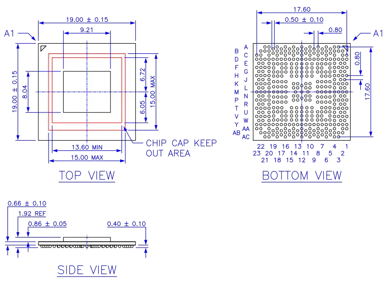
Package Diagram
All dimensions in millimeters.
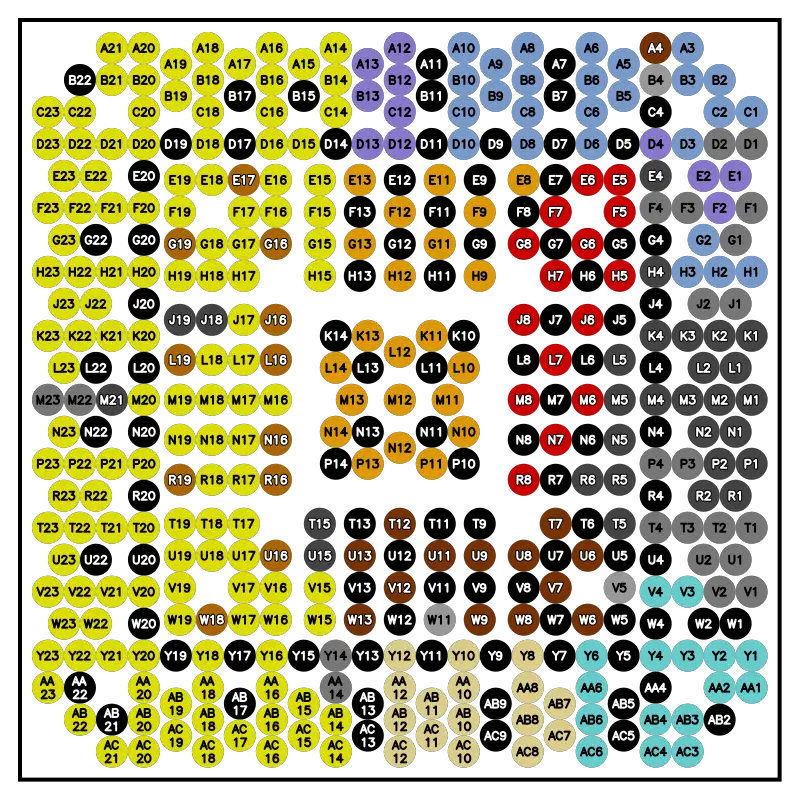
BGA-413 package pin (ball) numbering.
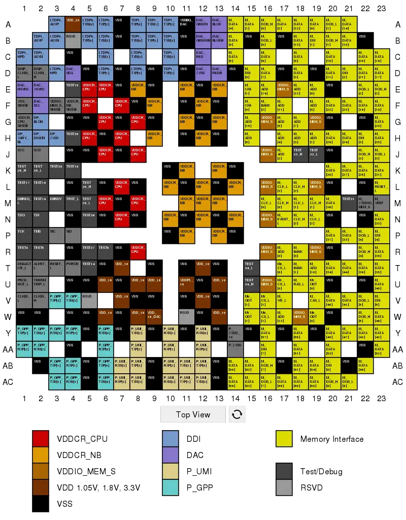
Pin Map
Pin Description
| Signal | Description |
|---|---|
| ALERT_L | Programmable pin that can indicate different events, including a SB-TSI interrupt |
| CLKIN_H/L | 100 MHz PLL Differential Reference Clock |
| DAC_BLUE, DAC_BLUEB | Blue for Video Monitor Output |
| DAC_GREEN, DAC_GREENB | Green for Video Monitor Output |
| DAC_HSYNC, DAC_VSYNC | Display Horizontal, Vertical Sync |
| DAC_RED, DAC_REDB | Red for Video Monitor Output |
| DAC_SCL, DAC_SDA | I2C Clock, Data for Display (to video monitor) |
| DAC_ZVSS | Compensation Resistor to DAC Ground Pin |
| DBREQ_L/DBRDY | Debug Request/Ready |
| DISP_CLKIN_H/L | 100 MHz Display Controller Reference Clock |
| DMAACTIVE_L | Indicated System DMA Activity |
| DP_BLON | Display Panel Backlight Enable |
| DP_DIGON | Display Panel Power Enable |
| DP_VARY_BL | Display Backlight Brightness Control |
| DP_ZVSS | Compensation Resistor to VSS |
| LTDP0/TDP1_AUXP/N | DisplayPort Auxiliary Channel |
| LTDP0/TDP1_HPD | DisplayPort Hot Plug Detect |
| LTDP0/TDP1_TXP/N[3:0] | DisplayPort Differential Transmitter |
| M0_CS_L[1:0], M1_CS_L[1:0] | DRAM Chip Selects |
| M0_ODT[1:0], M1_ODT[1:0] | DRAM Enable Pin for On Die Termination |
| M_ADD[15:0] | DRAM Column/Row Address |
| M_BANK[2:0] | DRAM Bank Address |
| M_CAS_L | DRAM Column Address Strobe |
| M_CKE[1:0] | DRAM Clock Enable |
| M_CLK_H/L[3:0] | DRAM Differential Clock |
| M_DATA[63:0] | DRAM Interface Data Bus |
| M_DM[7:0] | DRAM Data Mask |
| M_DQS_H/L[7:0] | DRAM Differential Data Strobe |
| M_EVENT_L | DRAM Thermal Event |
| M_RAS_L | DRAM Row Address Strobe |
| M_RESET_L | DRAM Reset Pin for Suspend-to-RAM Power Management Mode |
| M_VREF | Memory Interface Voltage Reference |
| M_WE_L | DRAM Write Enable |
| M_ZVDDIO_MEM_S | Compensation Resistor to VDDIO |
| PROCHOT_L | Processor in HTC-active state input/output |
| PWROK | Voltages and CLKIN have reached specified operation |
| P_GPP_TX/RXP/N[3:0] | General Purpose External PCIe Transmit/Receive Data Differential Pairs |
| P_UMI_TX/RXP/N[3:0] | Unified Media Interface Transmit/Receive Data Differential Pairs |
| P_ZVDD_10 | Compensation Resistor to P_VDD_10 Power Supply |
| P_ZVSS | Compensation Resistor to VSS |
| RESET_L | Processor Reset |
| RSVD | Reserved |
| SIC, SID | Sideband Temperature Sensor Interface Clock, Data |
| SVC, SVD | Serial VID Interface Clock, Data |
| TCK, TDI, TDO, TMS, TRST_L | JTAG interface |
| TEST* | Test signal |
| THERMTRIP_L | Thermal Sensor Trip output |
| VDDCR_CPU_SENSE | VDDCR_CPU Voltage Monitor Pin |
| VDDCR_CPU | Core Power Supply |
| VDDCR_NB_SENSE | VDDCR_NB Voltage Monitor Pin |
| VDDCR_NB | Northbridge Power Supply |
| VDDIO_MEM_S_SENSE | VDDIO_MEM_S Voltage Monitor Pin |
| VDDIO_MEM_S | DDR SDRAM I/O Ring Power Supply |
| VDDPL_10 | 1.05 V Supply Pin for System PLL |
| VDD_10 | 1.05 V Supply Pins |
| VDD_18_DAC | 1.8 V Supply Pin for DAC |
| VDD_18 | 1.8 V Supply Pins |
| VDD_33 | 3.3 V Supply Pin |
| VSSBG_DAC | DAC Ground |
| VSS_SENSE | VSS Voltage Monitor Pin |
| VSS | Ground |
References
- "FT1 Processor Functional Data Sheet", AMD Publ. #44444, Rev. 2.05, November 2010
- "BIOS and Kernel Developer’s Guide (BKDG) for AMD Family 14h Models 00h-0Fh Processors", AMD Publ. 43170, Rev. 3.13, February 17, 2012
- "Revision Guide for AMD Family 14h Models 00h-0Fh Processors", AMD Publ. #47534, Rev. 3.18, February 2013
See also
Facts about "Package FT1 - AMD"
| designer | AMD + |
| first launched | January 4, 2011 + |
| instance of | package + |
| market segment | Mobile + and Embedded + |
| microarchitecture | Bobcat + |
| name | FT1 + |
| package | FT1 + and UOB413 + |
| package contacts | 413 + |
| package height | 1.92 mm (0.0756 in) + |
| package length | 19 mm (1.9 cm, 0.748 in) + |
| package pitch | 0.8 mm (0.0315 in) + |
| package type | FC-OBGA + |
| package width | 19 mm (1.9 cm, 0.748 in) + |
| tdp | 18 W (18,000 mW, 0.0241 hp, 0.018 kW) + |


