| Edit Values | |
| Zen+ µarch | |
| General Info | |
| Arch Type | CPU |
| Designer | AMD |
| Manufacturer | GlobalFoundries |
| Introduction | April 13, 2018 |
| Process | 12 nm |
| Core Configs | 2, 4, 6, 8, 12, 16 |
| Pipeline | |
| Type | Superscalar |
| OoOE | Yes |
| Speculative | Yes |
| Reg Renaming | Yes |
| Stages | 19 |
| Decode | 4-way |
| Instructions | |
| ISA | x86-64 |
| Extensions | MOVBE, MMX, SSE, SSE2, SSE3, SSSE3, SSE4.1, SSE4.2, POPCNT, AVX, AVX2, AES, PCLMUL, RDRND, F16C, BMI, BMI2, RDSEED, ADCX, PREFETCHW, CLFLUSHOPT, XSAVE, SHA, CLZERO |
| Cache | |
| L1I Cache | 64 KiB/core 4-way set associative |
| L1D Cache | 32 KiB/core 8-way set associative |
| L2 Cache | 512 KiB/core 8-way set associative |
| L3 Cache | 2 MiB/core 16-way set associative |
| Cores | |
| Core Names | Pinnacle Ridge, Colfax |
| Succession | |
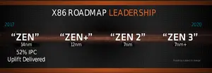
Zen+ (Zen Plus) is the successor to Zen, a 12 nm microarchitecture designed by AMD and introduced in 2018 for the mainstream PC, enthusiast, and server markets. Zen+ is expected to be replaced by Zen 2 in 2019.
Zen+ based processors are sold under the brand Ryzen 2nd Generation.
Contents
History
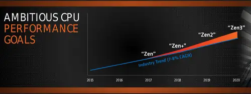
Zen+ succeeded Zen in April of 2018. Zen+ features the same core as Zen but takes advantage of the new GlobalFoundries' 12nm process to deliver higher clock speeds and improved power consumption. Zen+ was initially mentioned by AMD's senior fellow and lead architect of Zen, Michael Clark, during Hot Chips 28 in 2016 as part of AMD's continuing commitment in the high-performance computing market.
Codenames
| Core | C/T | Target |
|---|---|---|
| Colfax | Up to 32/64 | Enthusiasts market processors |
| Pinnacle Ridge | Up to 8/16 | Mainstream to high-end desktops & enthusiasts market processors |
Process Technology
- See also: 12 nm process
Zen+ is manufactured on Global Foundries' 12 nm process Leading-Performance (12LP), an enhanced version of their 14nm process. The enhanced process provides up to 15% higher density or up to 10% higher performance. 12LP brings around a 10% frequency bump for the Ryzen lineup at the same power envelopes.
Note that AMD did not switch to standard libraries and instead chose to get whatever added performance they could get from the same physical design as 14 nm. This also means some performance was left on the table and the die size is exactly the same as Zen.
Compatibility
Linux added initial support for Zen starting with Linux Kernel 4.10. Microsoft officially only supports Zen on Windows 10. Windows 7 and 8 drivers are available for many mainboards. But drivers must be integrated into the installation image or installed first before switching to a Zen-based system. Otherwise support for any kind of USB device like keyboard and mouse would be missing.
| Vendor | OS | Version | Notes |
|---|---|---|---|
| Microsoft | Windows | Windows 7 | No Support |
| Windows 8 | No Support | ||
| Windows 10 | Support | ||
| Linux | Linux | Kernel 4.10 | Initial Support |
Compiler support
Zen+ is largely the same architecture as Zen and thus uses the same compiler switches.
| Compiler | Arch-Specific | Arch-Favorable |
|---|---|---|
| AOCC | ‐march=znver1 |
-mtune=znver1
|
| GCC | -march=znver1 |
-mtune=znver1
|
| LLVM | -march=znver1 |
-mtune=znver1
|
| Visual Studio | /arch:AVX2 |
? |
CPUID
| Core | Extended Family |
Family | Extended Model |
Model |
|---|---|---|---|---|
| Pinnacle Ridge | 0x8 | 0xF | 0x0 | 0x8 |
| Family 23 Model 8 | ||||
Release Dates
AMD launched 2nd generation Ryzen on the 19th April of 2018. 2nd Generation Ryzen Threadripper and Ryzen PRO processors will launch in the second half of 2018.
Architecture
Serving as a light refresh over Zen, those processors have around ten percent higher base frequency for the same power envelope.
Key changes from Zen
- ~10% higher clock frequency
- ~3% single-thread IPC improvement
- 12 nm process (from 14 nm)
- Precision Boost 2 (from Precision Boost)
- Uses linear model based on temp/current/voltage feedbacks (From 2-core/all-core boost model)
- XFR 2 (from XFR 1)
- Cache
- Improved cache prefetch
- 12 cycle L2 latency for mainstream desktop (from 17 cycles)
- Memory
- Higher DDR4 transfer rate (2933 MT/s from 2666 MT/s)
- Mainstream chipsets (See § Sockets/Platform)
- X370 → X470
- New StoreMI Technology
- Lower Power
- Bug fixes
- OEM related issues resolved (unspecified)
- X370 → X470
Block Diagram
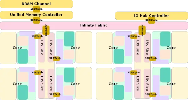
Entire SoC Overview
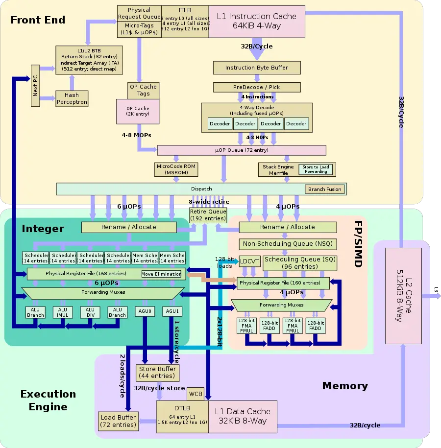
Individual Core
Memory Hierarchy
- Cache
- L0 µOP cache:
- 2,048 µOPs, 8-way set associative
- 32-sets, 8-µOP line size
- Parity protected
- 2,048 µOPs, 8-way set associative
- L1I Cache:
- 64 KiB 4-way set associative
- 256-sets, 64 B line size
- Shared by the two threads, per core
- Parity protected
- 64 KiB 4-way set associative
- L1D Cache:
- 32 KiB 8-way set associative
- 64-sets, 64 B line size
- Write-back policy
- 4-5 cycles latency for Int
- 7-8 cycles latency for FP
- SEC-DED ECC
- 32 KiB 8-way set associative
- L2 Cache:
- 512 KiB 8-way set associative
- 1,024-sets, 64 B line size
- Write-back policy
- Inclusive of L1
- 12 cycles latency
- DEC-TED ECC
- L3 Cache:
- Victim cache
- Summit Ridge, Naples: 8 MiB/CCX, shared across all cores.
- Raven Ridge: 4 MiB/CCX, shared across all cores.
- 16-way set associative
- 8,192-sets, 64 B line size
- 40 cycles latency
- DEC-TED ECC
- System DRAM:
- 2 channels per die
- Summit Ridge: up to PC4-21300U (DDR4-2666 UDIMM)
- Raven Ridge: up to PC4-23466U (DDR4-2933 UDIMM)
- Naples: up to PC4-21300L (DDR4-2666 RDIMM/LRDIMM)
- ECC support: x4 DRAM device failure correction (Chipkill), x8 SEC-DED ECC, Patrol and Demand scrubbing, Data poisoning
- L0 µOP cache:
Zen TLB consists of dedicated level one TLB for instruction cache and another one for data cache.
- TLBs
- ITLB
- 8 entry L0 TLB, all page sizes
- 64 entry L1 TLB, all page sizes
- 512 entry L2 TLB, no 1G pages
- Parity protected
- DTLB
- 64 entry L1 TLB, all page sizes
- 1,532-entry L2 TLB, no 1G pages
- Parity protected
- ITLB
Core
Pipeline
Zen+ pipeline is identical to Zen's.
Memory Subsystem
When AMD presented their paper at ISSCC 2018, WikiChip was able to confirm with AMD's SoC architect that Zen's L2 latency was always designed to be 12 cycles. In fact all Zen-based microprocessors (including EPYC, Ryzen Threadripper, and Zen-based APUs) have an L2 latency of 12 cycles for all access patterns. Only mainstream Zen-based Ryzen processors (i.e., Summit Ridge) have a latency of 17 cycles. The problem has been sorted out with Zen+.
Die
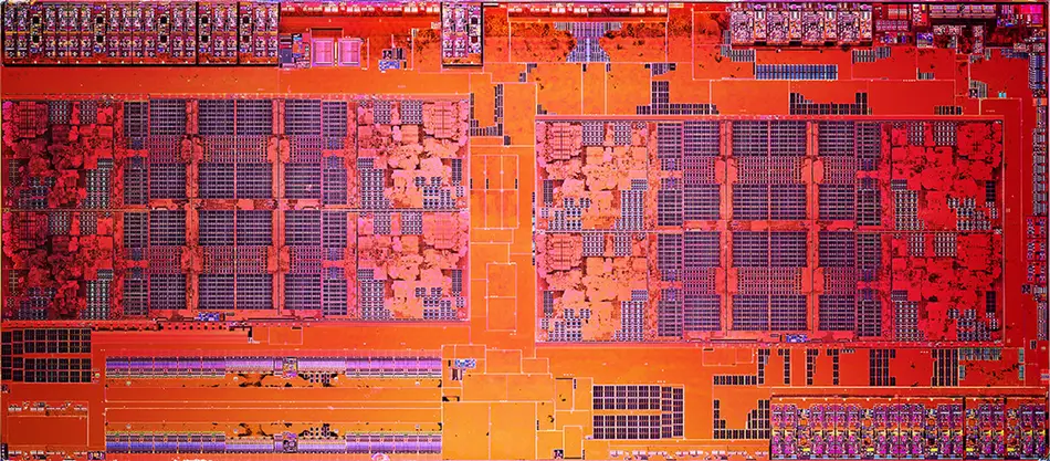
Zeppelin
- 12 nm process
- 12 metal layers
- 4,800,000,000 transistors
- ~22.058 mm x ~9.655 mm (Estimated)
- 212.97 mm² die size
Sockets/Platform
All Zen+-based mainstream consumer microprocessors utilizes AMD's Socket AM4, a unified socket infrastructure. All those processors are a complete system on a chip integrating the northbridge (memory controller) and the southbridge including 16 PCIe lanes for the GPU, 4 PCIe lanes for the NVMe/SATA controllers as well as USB 3.0. The chipset, however, extends the processor with a number of additional connections beyond that offered by the SoC.
| Socket AM4 Platform [Edit] | ||||||||||
|---|---|---|---|---|---|---|---|---|---|---|
| Segment | Chipset | USB | SATA | SATAe | PCIe | RAID | Dual PCIe | Overclocking | ||
| 3.1 G1 | 3.1 G2 | 2.0 | ||||||||
| 500-series (Zen+, Zen 2, Zen 3) | ||||||||||
| Mainstream | B550 | 2 | 6 | 6 | 8 + 4x NVME | 0 | 16x Gen4 | 0,1,10 | ✔ | ✔ |
| Enthusiast | X570 | 0 | 8 | 4 | 14 + 4x NVME | 0 | 16x Gen4 | 0,1,10 | ||
| 400-series (Zen+) | ||||||||||
| Mainstream | B450 | 2 | 2 | 6 | 6 + 4x NVME | 1 | 6x Gen3 | 0,1,10 | ✘ | ✔ |
| Enthusiast | X470 | 6 | 2 | 6 | 10 + 4x NVME | 2 | 8x Gen3 | 0,1,10 | ✔ | |
| 300-series (Zen) | ||||||||||
| Small Form Factor | A300, B300 | 4 | 0 | 0 | 2 + 2x NVMe | 1 | 4x Gen3 | 0,1 | ✘ | |
| X300 | 4 | 0 | 0 | 2 + 2x NVMe | 1 | 4x Gen3 | 0,1 | ✔ | ||
| Entry-level | A320 | 6 | 1 | 6 | 4 + 2x NVMe | 2 | 4x Gen2 | 0,1,10 | ✘ | ✘ |
| Mainstream | B350 | 6 | 2 | 6 | 4 + 2x NVMe | 2 | 6x Gen2 | 0,1,10 | ✔ | |
| Enthusiast | X370 | 6 | 2 | 6 | 6 + 2x NVMe | 2 | 8x Gen2 | 0,1,10 | ✔ | |
StoreMI
A new feature AMD has added to the 400-series chipset is "StoreMI", a technology with very similar capabilities to Intel's Smart Response Technology which attempts to combine the benefits of fast, but expensive, SSDs along with cheap high-capacity, but slow, HDDs. StoreMI combines the two storage devices into a single virtual drive (single letter drive on Windows) and automatically manages and moves the data across the drives. Essentially, the chipset uses the SSD as a cache for traditional hard drives. The idea is to keep the most recent and most accessed data on the SSD in order to improve real-world responsiveness while keeping the less used data in the slower mechanical hard disk in order to preserve the capacity of the SSD. It’s worth noting that this hierarchy of secondary storage devices can actually extend to main memory. Up to 2 GiB of RAM may be configured and reserved as another level of cache for the HDD on top of the SSD.
All Zen+ Chips
| List of all Zen+ based Processors | |||||||||||
|---|---|---|---|---|---|---|---|---|---|---|---|
| Model | Price | Launched | Family | Core | Cores | Threads | L2$ | L3$ | Frequency | Boost | TDP |
| PRO 300GE | 30 September 2019 | Athlon | Picasso | 2 | 4 | 1 MiB 1,024 KiB 1,048,576 B 9.765625e-4 GiB | 4 MiB 4,096 KiB 4,194,304 B 0.00391 GiB | 3.4 GHz 3,400 MHz 3,400,000 kHz | 35 W 35,000 mW 0.0469 hp 0.035 kW | ||
| PRO 300U | 8 April 2019 | Athlon | Picasso | 2 | 4 | 1 MiB 1,024 KiB 1,048,576 B 9.765625e-4 GiB | 4 MiB 4,096 KiB 4,194,304 B 0.00391 GiB | 2.4 GHz 2,400 MHz 2,400,000 kHz | 15 W 15,000 mW 0.0201 hp 0.015 kW | ||
| 2300X | 10 September 2018 | Ryzen 3 | Pinnacle Ridge | 4 | 4 | 2 MiB 2,048 KiB 2,097,152 B 0.00195 GiB | 8 MiB 8,192 KiB 8,388,608 B 0.00781 GiB | 3.5 GHz 3,500 MHz 3,500,000 kHz | 65 W 65,000 mW 0.0872 hp 0.065 kW | ||
| 3200G | $ 99.00 € 89.10 £ 80.19 ¥ 10,229.67 | 7 July 2019 | Ryzen 3 | Picasso | 4 | 4 | 2 MiB 2,048 KiB 2,097,152 B 0.00195 GiB | 4 MiB 4,096 KiB 4,194,304 B 0.00391 GiB | 3.6 GHz 3,600 MHz 3,600,000 kHz | 65 W 65,000 mW 0.0872 hp 0.065 kW | |
| 3200U | 6 January 2019 | Ryzen 3 | Picasso | 2 | 4 | 1 MiB 1,024 KiB 1,048,576 B 9.765625e-4 GiB | 4 MiB 4,096 KiB 4,194,304 B 0.00391 GiB | 2.6 GHz 2,600 MHz 2,600,000 kHz | 15 W 15,000 mW 0.0201 hp 0.015 kW | ||
| 3300U | 6 January 2019 | Ryzen 3 | Picasso | 4 | 4 | 2 MiB 2,048 KiB 2,097,152 B 0.00195 GiB | 4 MiB 4,096 KiB 4,194,304 B 0.00391 GiB | 2.1 GHz 2,100 MHz 2,100,000 kHz | 15 W 15,000 mW 0.0201 hp 0.015 kW | ||
| PRO 3200G | 30 September 2019 | Ryzen 3 | Picasso | 4 | 4 | 2 MiB 2,048 KiB 2,097,152 B 0.00195 GiB | 4 MiB 4,096 KiB 4,194,304 B 0.00391 GiB | 3.6 GHz 3,600 MHz 3,600,000 kHz | 65 W 65,000 mW 0.0872 hp 0.065 kW | ||
| PRO 3200GE | 30 September 2019 | Ryzen 3 | Picasso | 4 | 4 | 2 MiB 2,048 KiB 2,097,152 B 0.00195 GiB | 4 MiB 4,096 KiB 4,194,304 B 0.00391 GiB | 3.3 GHz 3,300 MHz 3,300,000 kHz | 35 W 35,000 mW 0.0469 hp 0.035 kW | ||
| PRO 3300U | 8 April 2019 | Ryzen 3 | Picasso | 4 | 4 | 2 MiB 2,048 KiB 2,097,152 B 0.00195 GiB | 4 MiB 4,096 KiB 4,194,304 B 0.00391 GiB | 2.1 GHz 2,100 MHz 2,100,000 kHz | 15 W 15,000 mW 0.0201 hp 0.015 kW | ||
| 2500X | 10 September 2018 | Ryzen 5 | Pinnacle Ridge | 4 | 8 | 2 MiB 2,048 KiB 2,097,152 B 0.00195 GiB | 8 MiB 8,192 KiB 8,388,608 B 0.00781 GiB | 3.6 GHz 3,600 MHz 3,600,000 kHz | 65 W 65,000 mW 0.0872 hp 0.065 kW | ||
| 2600 | $ 170.00 € 153.00 £ 137.70 ¥ 17,566.10 | 19 April 2018 | Ryzen 5 | Pinnacle Ridge | 6 | 12 | 3 MiB 3,072 KiB 3,145,728 B 0.00293 GiB | 16 MiB 16,384 KiB 16,777,216 B 0.0156 GiB | 3.4 GHz 3,400 MHz 3,400,000 kHz | 65 W 65,000 mW 0.0872 hp 0.065 kW | |
| 2600E | 10 September 2018 | Ryzen 5 | Pinnacle Ridge | 6 | 12 | 3 MiB 3,072 KiB 3,145,728 B 0.00293 GiB | 16 MiB 16,384 KiB 16,777,216 B 0.0156 GiB | 3.1 GHz 3,100 MHz 3,100,000 kHz | 45 W 45,000 mW 0.0603 hp 0.045 kW | ||
| 2600X | $ 229.00 € 206.10 £ 185.49 ¥ 23,662.57 | 19 April 2018 | Ryzen 5 | Pinnacle Ridge | 6 | 12 | 3 MiB 3,072 KiB 3,145,728 B 0.00293 GiB | 16 MiB 16,384 KiB 16,777,216 B 0.0156 GiB | 3.6 GHz 3,600 MHz 3,600,000 kHz | 95 W 95,000 mW 0.127 hp 0.095 kW | |
| 3400G | 7 July 2019 | Ryzen 5 | Picasso | 4 | 8 | 2 MiB 2,048 KiB 2,097,152 B 0.00195 GiB | 4 MiB 4,096 KiB 4,194,304 B 0.00391 GiB | 3.7 GHz 3,700 MHz 3,700,000 kHz | 65 W 65,000 mW 0.0872 hp 0.065 kW | ||
| 3500U | 6 January 2019 | Ryzen 5 | Picasso | 4 | 8 | 2 MiB 2,048 KiB 2,097,152 B 0.00195 GiB | 4 MiB 4,096 KiB 4,194,304 B 0.00391 GiB | 2.1 GHz 2,100 MHz 2,100,000 kHz | 15 W 15,000 mW 0.0201 hp 0.015 kW | ||
| 3550H | 6 January 2019 | Ryzen 5 | Picasso | 4 | 8 | 2 MiB 2,048 KiB 2,097,152 B 0.00195 GiB | 4 MiB 4,096 KiB 4,194,304 B 0.00391 GiB | 2.1 GHz 2,100 MHz 2,100,000 kHz | 35 W 35,000 mW 0.0469 hp 0.035 kW | ||
| 3580U | October 2019 | Ryzen 5 | Picasso | 4 | 8 | 2 MiB 2,048 KiB 2,097,152 B 0.00195 GiB | 4 MiB 4,096 KiB 4,194,304 B 0.00391 GiB | 2.1 GHz 2,100 MHz 2,100,000 kHz | 15 W 15,000 mW 0.0201 hp 0.015 kW | ||
| PRO 2600 | 6 September 2018 | Ryzen 5 | Pinnacle Ridge | 6 | 12 | 3 MiB 3,072 KiB 3,145,728 B 0.00293 GiB | 16 MiB 16,384 KiB 16,777,216 B 0.0156 GiB | 3.4 GHz 3,400 MHz 3,400,000 kHz | 65 W 65,000 mW 0.0872 hp 0.065 kW | ||
| PRO 3400G | 30 September 2019 | Ryzen 5 | Picasso | 4 | 8 | 2 MiB 2,048 KiB 2,097,152 B 0.00195 GiB | 4 MiB 4,096 KiB 4,194,304 B 0.00391 GiB | 3.7 GHz 3,700 MHz 3,700,000 kHz | 65 W 65,000 mW 0.0872 hp 0.065 kW | ||
| PRO 3400GE | 30 September 2019 | Ryzen 5 | Picasso | 4 | 8 | 2 MiB 2,048 KiB 2,097,152 B 0.00195 GiB | 4 MiB 4,096 KiB 4,194,304 B 0.00391 GiB | 3.3 GHz 3,300 MHz 3,300,000 kHz | 35 W 35,000 mW 0.0469 hp 0.035 kW | ||
| PRO 3500U | 8 April 2019 | Ryzen 5 | Picasso | 4 | 8 | 2 MiB 2,048 KiB 2,097,152 B 0.00195 GiB | 4 MiB 4,096 KiB 4,194,304 B 0.00391 GiB | 2.1 GHz 2,100 MHz 2,100,000 kHz | 15 W 15,000 mW 0.0201 hp 0.015 kW | ||
| 2700 | $ 299.00 € 269.10 £ 242.19 ¥ 30,895.67 | 19 April 2018 | Ryzen 7 | Pinnacle Ridge | 8 | 16 | 4 MiB 4,096 KiB 4,194,304 B 0.00391 GiB | 16 MiB 16,384 KiB 16,777,216 B 0.0156 GiB | 3.2 GHz 3,200 MHz 3,200,000 kHz | 65 W 65,000 mW 0.0872 hp 0.065 kW | |
| 2700E | 10 September 2018 | Ryzen 7 | Pinnacle Ridge | 8 | 16 | 4 MiB 4,096 KiB 4,194,304 B 0.00391 GiB | 16 MiB 16,384 KiB 16,777,216 B 0.0156 GiB | 2.8 GHz 2,800 MHz 2,800,000 kHz | 45 W 45,000 mW 0.0603 hp 0.045 kW | ||
| 2700X Gold Edition | $ 329.00 € 296.10 £ 266.49 ¥ 33,995.57 | 29 April 2019 | Ryzen 7 | Pinnacle Ridge | 8 | 16 | 4 MiB 4,096 KiB 4,194,304 B 0.00391 GiB | 16 MiB 16,384 KiB 16,777,216 B 0.0156 GiB | 3.7 GHz 3,700 MHz 3,700,000 kHz | 105 W 105,000 mW 0.141 hp 0.105 kW | |
| 2700X | $ 329.00 € 296.10 £ 266.49 ¥ 33,995.57 | 19 April 2018 | Ryzen 7 | Pinnacle Ridge | 8 | 16 | 4 MiB 4,096 KiB 4,194,304 B 0.00391 GiB | 16 MiB 16,384 KiB 16,777,216 B 0.0156 GiB | 3.7 GHz 3,700 MHz 3,700,000 kHz | 105 W 105,000 mW 0.141 hp 0.105 kW | |
| 3700U | 6 January 2019 | Ryzen 7 | Picasso | 4 | 8 | 2 MiB 2,048 KiB 2,097,152 B 0.00195 GiB | 4 MiB 4,096 KiB 4,194,304 B 0.00391 GiB | 2.3 GHz 2,300 MHz 2,300,000 kHz | 15 W 15,000 mW 0.0201 hp 0.015 kW | ||
| 3750H | 6 January 2019 | Ryzen 7 | Picasso | 4 | 8 | 2 MiB 2,048 KiB 2,097,152 B 0.00195 GiB | 4 MiB 4,096 KiB 4,194,304 B 0.00391 GiB | 2.3 GHz 2,300 MHz 2,300,000 kHz | 35 W 35,000 mW 0.0469 hp 0.035 kW | ||
| 3780U | October 2019 | Ryzen 7 | Picasso | 4 | 8 | 2 MiB 2,048 KiB 2,097,152 B 0.00195 GiB | 4 MiB 4,096 KiB 4,194,304 B 0.00391 GiB | 2.3 GHz 2,300 MHz 2,300,000 kHz | 15 W 15,000 mW 0.0201 hp 0.015 kW | ||
| PRO 2700 | 6 September 2018 | Ryzen 7 | Pinnacle Ridge | 8 | 16 | 4 MiB 4,096 KiB 4,194,304 B 0.00391 GiB | 16 MiB 16,384 KiB 16,777,216 B 0.0156 GiB | 3.2 GHz 3,200 MHz 3,200,000 kHz | 65 W 65,000 mW 0.0872 hp 0.065 kW | ||
| PRO 2700X | 6 September 2018 | Ryzen 7 | Pinnacle Ridge | 8 | 16 | 4 MiB 4,096 KiB 4,194,304 B 0.00391 GiB | 16 MiB 16,384 KiB 16,777,216 B 0.0156 GiB | 3.6 GHz 3,600 MHz 3,600,000 kHz | 105 W 105,000 mW 0.141 hp 0.105 kW | ||
| PRO 3700U | 8 April 2019 | Ryzen 7 | Picasso | 4 | 8 | 2 MiB 2,048 KiB 2,097,152 B 0.00195 GiB | 4 MiB 4,096 KiB 4,194,304 B 0.00391 GiB | 2.3 GHz 2,300 MHz 2,300,000 kHz | 15 W 15,000 mW 0.0201 hp 0.015 kW | ||
| 2920X | $ 649.00 € 584.10 £ 525.69 ¥ 67,061.17 | 29 October 2018 | Ryzen Threadripper | Colfax | 12 | 24 | 6 MiB 6,144 KiB 6,291,456 B 0.00586 GiB | 32 MiB 32,768 KiB 33,554,432 B 0.0313 GiB | 3.5 GHz 3,500 MHz 3,500,000 kHz | 180 W 180,000 mW 0.241 hp 0.18 kW | |
| 2950X | $ 899.00 € 809.10 £ 728.19 ¥ 92,893.67 | 31 August 2018 | Ryzen Threadripper | Colfax | 16 | 32 | 8 MiB 8,192 KiB 8,388,608 B 0.00781 GiB | 32 MiB 32,768 KiB 33,554,432 B 0.0313 GiB | 3.5 GHz 3,500 MHz 3,500,000 kHz | 180 W 180,000 mW 0.241 hp 0.18 kW | |
| 2970WX | $ 1,299.00 € 1,169.10 £ 1,052.19 ¥ 134,225.67 | 29 October 2018 | Ryzen Threadripper | Colfax | 24 | 48 | 12 MiB 12,288 KiB 12,582,912 B 0.0117 GiB | 64 MiB 65,536 KiB 67,108,864 B 0.0625 GiB | 3 GHz 3,000 MHz 3,000,000 kHz | 250 W 250,000 mW 0.335 hp 0.25 kW | |
| 2990WX | $ 1,799.00 € 1,619.10 £ 1,457.19 ¥ 185,890.67 | 13 August 2018 | Ryzen Threadripper | Colfax | 32 | 64 | 16 MiB 16,384 KiB 16,777,216 B 0.0156 GiB | 64 MiB 65,536 KiB 67,108,864 B 0.0625 GiB | 3 GHz 3,000 MHz 3,000,000 kHz | 250 W 250,000 mW 0.335 hp 0.25 kW | |
| Count: 35 | |||||||||||
References
- AMD CES Tech Day 2018, Jim Anderson
- AMD CES Tech Day 2018, Lisa Su
- AMD CES Tech Day 2018, Mark Papermaster
Documents
See Also
- Intel Coffee Lake
| codename | Zen+ + |
| core count | 2 +, 4 +, 6 +, 8 +, 12 + and 16 + |
| designer | AMD + |
| first launched | April 13, 2018 + |
| full page name | amd/microarchitectures/zen+ + |
| instance of | microarchitecture + |
| instruction set architecture | x86-64 + |
| manufacturer | GlobalFoundries + |
| microarchitecture type | CPU + |
| name | Zen+ + |
| pipeline stages | 19 + |
| process | 12 nm (0.012 μm, 1.2e-5 mm) + |
