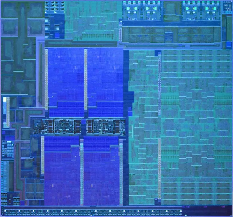
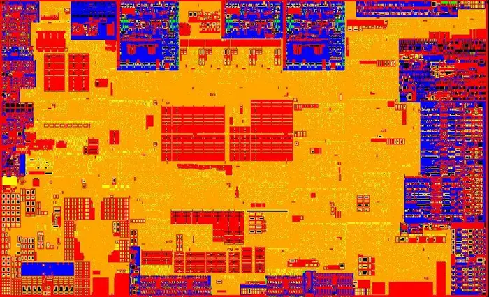
(→Die) |
|||
| (47 intermediate revisions by 6 users not shown) | |||
| Line 5: | Line 5: | ||
|designer=Intel | |designer=Intel | ||
|manufacturer=Intel | |manufacturer=Intel | ||
| − | |introduction=2019 | + | |introduction=May 27, 2019 |
|process=10 nm | |process=10 nm | ||
| + | |cores=2 | ||
| + | |cores 2=4 | ||
| + | |type=Superscalar | ||
| + | |oooe=Yes | ||
| + | |speculative=Yes | ||
| + | |renaming=Yes | ||
| + | |stages min=14 | ||
| + | |stages max=19 | ||
| + | |decode=5-way | ||
|isa=x86-64 | |isa=x86-64 | ||
| + | |extension=MOVBE | ||
| + | |extension 2=MMX | ||
| + | |extension 3=SSE | ||
| + | |extension 4=SSE2 | ||
| + | |extension 5=SSE3 | ||
| + | |extension 6=SSSE3 | ||
| + | |extension 7=SSE4.1 | ||
| + | |extension 8=SSE4.2 | ||
| + | |extension 9=POPCNT | ||
| + | |extension 10=AVX | ||
| + | |extension 11=AVX2 | ||
| + | |extension 12=AES | ||
| + | |extension 13=PCLMUL | ||
| + | |extension 14=FSGSBASE | ||
| + | |extension 15=RDRND | ||
| + | |extension 16=FMA3 | ||
| + | |extension 17=F16C | ||
| + | |extension 18=BMI | ||
| + | |extension 19=BMI2 | ||
| + | |extension 20=VT-x | ||
| + | |extension 21=VT-d | ||
| + | |extension 22=TXT | ||
| + | |extension 23=TSX | ||
| + | |extension 24=RDSEED | ||
| + | |extension 25=ADCX | ||
| + | |extension 26=PREFETCHW | ||
| + | |extension 27=CLFLUSHOPT | ||
| + | |extension 28=XSAVE | ||
| + | |extension 29=SGX | ||
| + | |extension 30=MPX | ||
| + | |extension 31=AVX-512 | ||
|l1i=32 KiB | |l1i=32 KiB | ||
|l1i per=core | |l1i per=core | ||
| Line 14: | Line 54: | ||
|l1d per=core | |l1d per=core | ||
|l1d desc=12-way set associative | |l1d desc=12-way set associative | ||
| − | |||
|l2=512 KiB | |l2=512 KiB | ||
| − | |l2 per= | + | |l2 per=core |
| − | |l2 desc= | + | |l2 desc=8-way set associative |
|l3=2 MiB | |l3=2 MiB | ||
|l3 per=core | |l3 per=core | ||
| Line 30: | Line 69: | ||
|contemporary link=intel/microarchitectures/ice_lake_(server) | |contemporary link=intel/microarchitectures/ice_lake_(server) | ||
}} | }} | ||
| − | '''Ice Lake''' ('''ICL''') '''Client Configuration''' is [[Intel]]'s successor to {{\\|Cannon Lake}}, a [[10 nm]] [[microarchitecture]] for mainstream | + | '''Ice Lake''' ('''ICL''') '''Client Configuration''' is [[Intel]]'s successor to {{\\|Cannon Lake}}, a [[10 nm]] [[microarchitecture]] for mainstream mobile devices. |
| + | |||
| + | For mobile devices, Ice Lake is branded as 10th Generation Core i3, i5, and i7 processors. | ||
== Codenames == | == Codenames == | ||
| Line 45: | Line 86: | ||
| <s>{{intel|Ice Lake S|l=core}}</s>? || <s>ICL-S</s> || <s>Performance-optimized lifestyle</s> || || <s>Desktop performance to value, AiOs, and minis</s> | | <s>{{intel|Ice Lake S|l=core}}</s>? || <s>ICL-S</s> || <s>Performance-optimized lifestyle</s> || || <s>Desktop performance to value, AiOs, and minis</s> | ||
|} | |} | ||
| + | |||
| + | == Lead == | ||
| + | * '''Ophir Edlis''' - Senior Principal Engineer & Lead Architect Ice Lake SoC | ||
== Process Technology== | == Process Technology== | ||
| − | {{ | + | {{main|10_nm_lithography_process#Intel|l1=Intel's 10-nanometer process}} |
| − | Ice Lake | + | Prolong delays with Intel's 10-nanometer process due to yield issues meant the terminology around that process was changed over time. Ice Lake is fabricated on Intel's second-generation enhanced [[10 nm process]]. Originally the process was meant to succeed first-generation which was used for {{\\|Cannon Lake}}. Unfortunately due to yield and performance reasons, Intel re-designated 2nd-generation as 1st-generation (ignoring {{\\|Cannon Lake}}), hence the plain name of "10nm" (without any pluses). |
| − | + | Intel says that Ice Lake is built on their learnings from their Cannon Lake chip which were largely treated as a learning vehicle. Between Cannon Lake and Ice Lake, a number of changes were made in order to improve the process for their products. One such change was the addition of an extra metal layer (originally said to be 12, is now presumably 13 on Ice Lake) in order to improve the power delivery of the chip. Additionally, they have improved the threshold voltage of the transistors as well as their MIM cap among other changes. | |
{{clear}} | {{clear}} | ||
| Line 97: | Line 141: | ||
** {{intel|Gen10|l=arch}} → {{intel|Gen11|l=arch}} graphics (''Gen10 was never productized'') | ** {{intel|Gen10|l=arch}} → {{intel|Gen11|l=arch}} graphics (''Gen10 was never productized'') | ||
** {{intel|Gen11|l=arch}} GPUs | ** {{intel|Gen11|l=arch}} GPUs | ||
| − | *** UHD Graphics 6xx (GT1) '''→''' UHD Graphics 9xx (GT2) ( | + | *** UHD Graphics 6xx (GT1) '''→''' UHD Graphics 9xx (GT2) (32 Execution Units, 2.67x EUs from {{\\|Gen9}}) |
*** UHD Graphics 6xx (GT2) '''→''' Iris Plus Graphics 9xx (GT2) (48-64 Execution Units, 2-2.6x EUs from {{\\|Gen9}}) | *** UHD Graphics 6xx (GT2) '''→''' Iris Plus Graphics 9xx (GT2) (48-64 Execution Units, 2-2.6x EUs from {{\\|Gen9}}) | ||
**** 1,024 GFLOPS @ 1 GHz (GT2) | **** 1,024 GFLOPS @ 1 GHz (GT2) | ||
| Line 103: | Line 147: | ||
** Gen 11.5 (from Gen9/Gen9.5) | ** Gen 11.5 (from Gen9/Gen9.5) | ||
** DisplayPort 1.4a with Display Stream Compression(DSC) (from DisplayPort 1.2) | ** DisplayPort 1.4a with Display Stream Compression(DSC) (from DisplayPort 1.2) | ||
| − | ** HDMI 2. | + | ** [[HDMI]] 2.0b (from HDMI 1.4) |
* IPU | * IPU | ||
** 4th Gen IPU (from 3rd Gen in {{\\|Skylake (client)|Skylake}}) | ** 4th Gen IPU (from 3rd Gen in {{\\|Skylake (client)|Skylake}}) | ||
| Line 109: | Line 153: | ||
** New concurrent image pipeline | ** New concurrent image pipeline | ||
** on-die MIPI interface | ** on-die MIPI interface | ||
| + | * New Integration | ||
| + | ** New Gaussian Neural Accelerator 1.0 (Added in {{\\|Cannon Lake}} but unclear to what extent) | ||
* I/O | * I/O | ||
** Thunderbolt 3 over Type-C | ** Thunderbolt 3 over Type-C | ||
| + | * Package | ||
| + | ** New Type3, Type4 packages | ||
| + | *** New thin-film magnetic inductors | ||
| + | *** 100μm [[copper pillars]] (from 130μm on [[14 nm]]) | ||
{{expand list}} | {{expand list}} | ||
====New instructions ==== | ====New instructions ==== | ||
| − | Ice Lake introduced a number of {{x86|extensions|new instructions}}. | + | {{see also|intel/microarchitectures/sunny_cove#New_instructions|l1=Sunny Cove § New Instructions}} |
| + | Ice Lake introduced a number of {{x86|extensions|new instructions}}. | ||
| + | |||
| + | * {{x86|SHA|<code>SHA</code>}} - [[Hardware acceleration]] for SHA hashing operations | ||
| + | * {{x86|CLWB|<code>CLWB</code>}} - Force cache line write-back without flush | ||
| + | * {{x86|RDPID|<code>RDPID</code>}} - Read Processor ID | ||
| + | * {{x86|AVX-512|<code>AVX-512</code>}} (originally introduced in {{\\|Skylake (Server)}} but only now in client) | ||
| + | ** {{x86|AVX512F|<code>AVX512F</code>}} - AVX-512 Foundation | ||
| + | ** {{x86|AVX512CD|<code>AVX512CD</code>}} - AVX-512 Conflict Detection | ||
| + | ** {{x86|AVX512BW|<code>AVX512BW</code>}} - AVX-512 Byte and Word | ||
| + | ** {{x86|AVX512DQ|<code>AVX512DQ</code>}} - AVX-512 Doubleword and Quadword | ||
| + | ** {{x86|AVX512VL|<code>AVX512VL</code>}} - AVX-512 Vector Length | ||
| + | * Additional {{x86|AVX-512}} extensions: | ||
| + | ** {{x86|AVX512VPOPCNTDQ|<code>AVX512VPOPCNTDQ</code>}} - AVX-512 Vector Population Count Doubleword and Quadword | ||
| + | ** {{x86|AVX512VNNI|<code>AVX512VNNI</code>}} - AVX-512 Vector Neural Network Instructions | ||
| + | ** {{x86|AVX512GFNI|<code>AVX512GFNI</code>}} - AVX-512 Galois Field New Instructions | ||
| + | ** {{x86|AVX512VAES|<code>AVX512VAES</code>}} - AVX-512 Vector AES | ||
| + | ** {{x86|AVX512VBMI2|<code>AVX512VBMI2</code>}} - AVX-512 Vector Bit Manipulation, Version 2 | ||
| + | ** {{x86|AVX512BITALG|<code>AVX512BITALG</code>}} - AVX-512 Bit Algorithms | ||
| + | ** {{x86|AVX512VPCLMULQDQ|<code>AVX512VPCLMULQDQ</code>}} - AVX-512 Vector Vector Carry-less Multiply | ||
| + | * {{x86|SSE_GFNI|<code>SSE_GFNI</code>}} - SSE-based Galois Field New Instructions | ||
| + | * {{x86|AVX_GFNI|<code>AVX_GFNI</code>}} - AVX-based Galois Field New Instructions | ||
| + | * Split Lock Detection - detection and cause an exception for split locks | ||
| + | * Fast Short REP MOV | ||
=== Block Diagram === | === Block Diagram === | ||
| Line 129: | Line 202: | ||
== Overview == | == Overview == | ||
| − | {{ | + | [[File:ice lake overview.svg|right|500px]] |
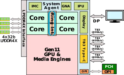
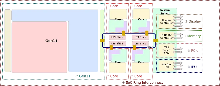
| + | The Ice Lake [[system on a chip]] is a [[10-nanometer]] SoC that is aimed at the mainstream to premium mobile and the thin-and-light market. The microprocessor consists of five major components: CPU cores, LLC, {{intel|ring interconnect}}, {{intel|system agent}}, and {{\\|Gen11}} graphics. While a lot of what Ice Lake provides is inherited from the prior generations, Intel claims that every IP on Ice Lake has been enhanced in one way or another. A major enhancement in Ice Lake over the prior generation is the integration of up to four {{\\|Sunny Cove}} cores which provide a significant uplift in IPC. Those cores also bring {{x86|AVX-512}} support for the client market. Those cores, along with the system agent and the GPU, are linked over Intel's {{intel|ring interconnect}}. The chip is fed through a new [[integrated memory controller]] that supports quad-channel 32-bit LPDDR4X memory, providing bandwidths in the range of 50-60 GB/s. Ice Lake has a new integrated GPU which is based on their {{\\|Gen11}} microarchitecture which provides a large improvement in graphics performance. | ||
| + | |||
| + | The system architecture in Ice Lake has been redesigned. Intel added a new Gaussian Neural Accelerator (GNA) for the acceleration of inference applications. There is a new 4th-generation [[image processing unit]] (IPU). Ice Lake integrates the entire Thunderbolt 3 I/O subsystem on-die, significantly simplifying support at the system level. Ice Lake has four Thunderbolt 3 ports. All four ports have the same capabilities and can be used simultaneously at full performance at up to 40 Gbps per port. Intel also upgraded the display engine to {{\\|Gen11}} with an improved display pipe that has a new Adaptive Sync and HDR-capable display pipes that support HDR 3 and DisplayPort 1.4, supporting error correction and compression. | ||
| + | |||
| + | Ice Lake chips integrate the {{intel|PCH}} die on-package communicating over the on-package interconnect (OPI). The new PCH The PCH has an expanded I/O support for PCIe, USB, SATA, as well as audio DSP for load power voice processing. It also integrates WiFi 6+ {{intel|CNVi}}. | ||
| + | |||
| + | On the platform level, there is a new integrated power delivery (FIVR) on both the PCH and the CPU which Intel says allows them to save on platform area by about 15% and it reduces the power delivery rails for the OEMs by roughly half. | ||
== Core == | == Core == | ||
{{empty section}} | {{empty section}} | ||
| − | == IPU == | + | == Integration == |
| + | Ice Lake integrates a number of additional components: | ||
| + | |||
| + | * 4th Generation [[image processing unit]] | ||
| + | * A new GNA [[neural processor]] | ||
| + | * A new Thunderbolt I/O subsystem | ||
| + | |||
| + | === GNA === | ||
| + | Ice Lake introduced a new low-power [[neural processor]] called the '''Gaussian Neural Accelerator v1.0''' ('''GNA''') which is integrated on the SoC and runs at very low power even when the GPU and CPUs are turned off. The GNA can be used for long-running tasks (e.g., real-time meeting transcription). The GNA can operate while the remaining parts of the SoC are in idle in order to have minimal impact on performance. | ||
| + | |||
| + | === IPU === | ||
Ice Lake incorporates 4th generation [[image processing unit]] (IPU). The IPU was first introduced with {{\\|Skylake (client)|Skylake}} mobile SoCs (note that those were 3rd gen). The 4th Gen IPU found in Ice Lake introduces a number of new enhancements. It introduces new support for 4K video capture at 30fps. There is also new hardware support for better de-noising which supports up to 16 megapixels stills in low light conditions. In addition for support more camera simultaneously, the IPU incorporates a new concurrent image pipeline, supporting multiple different processing from the same camera stream, allowing a single camera to take the functionality of multiple sensors. A common example of that is devices with both IR and RGB cameras in the laptop bezel which can now be changed to a single camera. Intel says they are exposing more registers from the IPU to software in order to provide more flexibility for applications that make use of that for machine learning. It’s also worth noting that Intel integrated the MIPI interface onto the processor as well. Previously that was found on the chipset. The change significantly improves the latency, a required attribute needed for more advanced ML-specific applications. Some of those changes are designed to form the foundation for future generations of improvements. | Ice Lake incorporates 4th generation [[image processing unit]] (IPU). The IPU was first introduced with {{\\|Skylake (client)|Skylake}} mobile SoCs (note that those were 3rd gen). The 4th Gen IPU found in Ice Lake introduces a number of new enhancements. It introduces new support for 4K video capture at 30fps. There is also new hardware support for better de-noising which supports up to 16 megapixels stills in low light conditions. In addition for support more camera simultaneously, the IPU incorporates a new concurrent image pipeline, supporting multiple different processing from the same camera stream, allowing a single camera to take the functionality of multiple sensors. A common example of that is devices with both IR and RGB cameras in the laptop bezel which can now be changed to a single camera. Intel says they are exposing more registers from the IPU to software in order to provide more flexibility for applications that make use of that for machine learning. It’s also worth noting that Intel integrated the MIPI interface onto the processor as well. Previously that was found on the chipset. The change significantly improves the latency, a required attribute needed for more advanced ML-specific applications. Some of those changes are designed to form the foundation for future generations of improvements. | ||
| + | |||
| + | === Thunderbolt IO subsystem === | ||
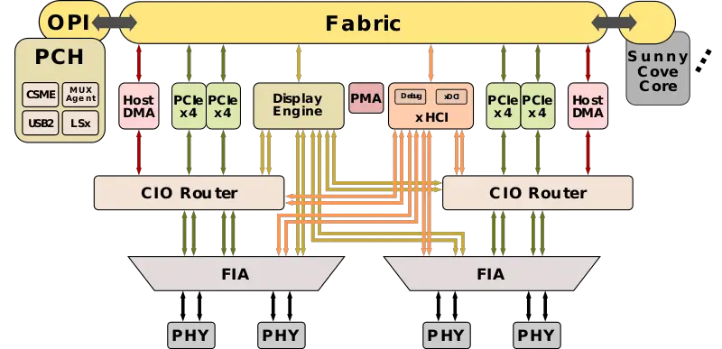
| + | By far the largest new integration in Ice Lake is the Thunderbolt I/O Subsystem. According to Intel, this is the largest integration they have done since the integration of the graphics processing unit in {{\\|Sandy Bridge}}. When Ice Lake was introduced, [[Thunderbolt 3]] was the fastest and most versatile connector that was available. Not only is it four times faster than USB 3.1, but it also supports additional peripherals over [[PCIe]], [[USB 3.1]], and DisplayPort, though note that only [[PCIe]] and [[DisplayPort]] tunnel over Thunderbolt while the [[USB 3.1]] is MUXed over them for direct USB support. | ||
| + | |||
| + | Ice Lake contains two modular FIAs, each one connect to a pair of Type-C ports for a total of four ports. The FIA can multiplex between a standard [[USB Type-C connector]] and a [[Thunderbolt connector]]. When serving USB 3.1, the FIA can serve as a standard USB Type-C connection, while when using PCIe/DP, it tunnels over Thunderbolt alternate mode. Each FIA is connected to the USB controller, Display Engine, and the CIO Router. The CIO Router is the actual Thunderbolt router and it can be thought of as a display engine as well. Ice Lake has a total of four PCIe controllers coming from four root complexes. Two PCIe controllers go to each of the CIOs. Previously, there was just a single PCIe controller going to the Titan Ridge controller, so there was effectively one PCIe controller for both ports. Compared to the prior generation, each port now effectively has double the bandwidth. | ||
| + | |||
| + | |||
| + | :[[File:ice lake io subsystem.svg|center|800px]] | ||
| + | |||
| + | |||
| + | {{center|'''Figure: Ice Lake Thunderbolt 3 I/O Subsystem'''}} | ||
| + | |||
| + | |||
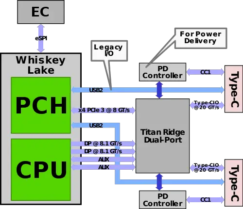
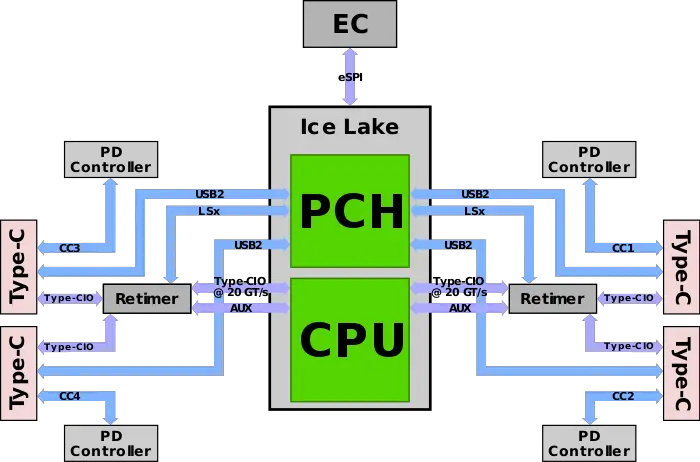
| + | Previously (e.g., with {{\\|Whiskey Lake}}), for OEMs to support Thunderbolt 3 in mobile devices, they had to use Intel's Titan Ridge controller. Titan Ridge was a discrete Thunderbolt 3 chip that came with either one or two dedicated [[Thunderbolt 3]] ports. In order to support everything that was necessary (e.g., legacy [[USB 2]] as well as high speed PCIe Gen 3), the controller was connected to both the CPU and the chipset. The chipset was connected over four PCIe Gen 3 lanes. The CPU had two DisplayPort connections. Each of those passed over four PCIe Gen 3 lanes. In order to offer legacy I/O support, a direct USB 2.0 link from the PCH went to the port. For charging capabilities, the port was also connected directly to a Power Deliver (PD) controller. In total, 17 PCIe Gen 3 lanes operating at around 8 GT/s were required between the Titan Ridge controller and the chipset and CPU. | ||
| + | |||
| + | Due to the design complexity introduced by the discrete controller, most mobile devices that made use of Titan Ridge only supported it on one side of the device - typically on the side of the device closer to the controller itself. | ||
| + | |||
| + | |||
| + | :[[File:intel type-c old.svg|center|500px]] | ||
| + | |||
| + | |||
| + | {{center|'''Figure: Thunderbolt 3 support using the Titan Ridge controller'''}} | ||
| + | |||
| + | |||
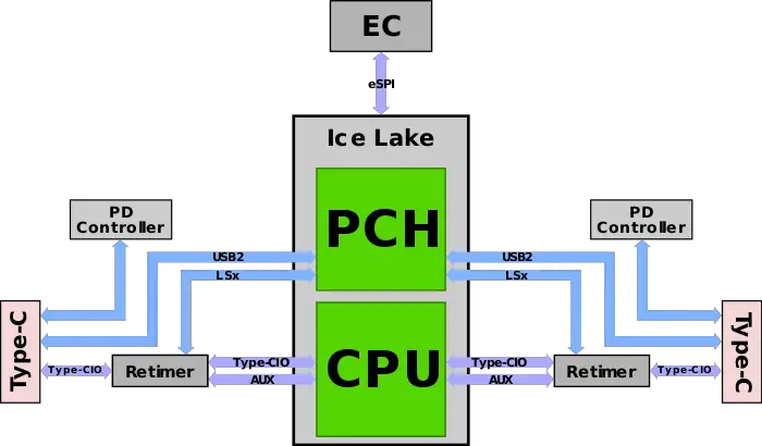
| + | With Ice Lake, Intel simplified the overall design considerably. The biggest change comes from the fact that most of the Titan Ridge logic has been integrated into the Ice Lake SoC itself, reducing board space, routing, and the overall [[bill of materials]]. Instead of the seventeen lanes that were required by the Titan Ridge controller, Ice Lake exposes just eight lanes – four lanes to each [[retimer]] which drive the signals to the connectors. Therefore, in total there are just eight lanes operating at 20 GT/s instead of seventeen lanes operating at 8 GT/s (note that number includes the 8.1 GT/s DP links). The reduction of lanes, along with their associated components such as the buffers, reduces the overall power consumption of the system. Intel stated that, depending on the exact device design, they saw a reduction of up to 300 mW per port when the port was fully utilized. Previously, the dual-port Titan Ridge controller had a TDP of up to 2.4 W, so the overall saving is fairly sizable. The additional power saving thus translates to better performance as more of the overall power budget can be allocated for the GPU and CPU instead of the I/O. | ||
| + | |||
| + | One of the other benefits of the Thunderbolt 3 integration is that half of the lanes can be exposed to each side of the device. With the Titan Ridge controller, offering Type-C ports on the side further from the controller was more complex and was quite rare and most OEMs simply opted to offer a legacy connector of some sort such as a USB 2.0 on that side. With Ice Lake, the direct Thunderbolt lanes that go to each retimer are easily exposed to both sides of the device, meaning, at least in theory, OEMs should have no problem offering symmetrical connections on both sides of the device. | ||
| + | |||
| + | |||
| + | :[[File:intel type-c ice lake.svg|center|700px]] | ||
| + | |||
| + | |||
| + | {{center|'''Figure: Thunderbolt 3 support on Ice Lake through the Thunderbolt 3 integration'''}} | ||
| + | |||
| + | |||
| + | Like Titan Ridge, each retimer supports two ports. The retimers themselves are still only sold by Intel but they are a fraction of the size, so there is also a modest board space saving advantage as well. Therefore, actually, the diagram above is almost identical when offering support for up to four Thunderbolt 3 ports, twice as many as most Titan Ridge-based designs. For full support, those additional ports just need a new dedicated USB 2 connection to the PCH, and in order to also offer charging capabilities through that port, you also need a PD controller. Premium-design laptop should, therefore, be able to have up to four Thunderbolt ports – each supporting everything from power delivery to the legacy I/O to the latest high-speed interfaces such as DisplayPort and USB 3.1. | ||
| + | |||
| + | |||
| + | :[[File:intel type-c ice lake 4p.svg|center|700px]] | ||
| + | |||
| + | |||
| + | {{center|'''Figure: Thunderbolt 3 support on Ice Lake through the Thunderbolt 3 integration<br>Full configuration with four ports and every feature through every port'''}} | ||
== Clock domains == | == Clock domains == | ||
| Line 148: | Line 280: | ||
[[File:ice lake soc clock domain block diagram.svg|850px]] | [[File:ice lake soc clock domain block diagram.svg|850px]] | ||
| + | |||
| + | == Power == | ||
| + | === Dynamic Tuning 2.0 === | ||
| + | {{main|intel/dynamic_tuning|l1=Intel Dynamic Tuning}} | ||
| + | {{empty section}} | ||
| + | |||
| + | == Packaging == | ||
| + | Ice Lake comes in two packagings. | ||
| + | |||
| + | {| class="wikitable" | ||
| + | |- | ||
| + | ! Package !! Type3 !! Type4 | ||
| + | |- | ||
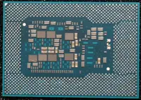
| + | | Core || {{intel|Ice Lake U|l=core}} || {{intel|Ice Lake Y|l=core}} | ||
| + | |- | ||
| + | | TDP || 15 W || 9 W | ||
| + | |- | ||
| + | | Dimensions || 50 x 25 x 1.3 mm || 26.5 x 18.5 x 1.0 mm | ||
| + | |- | ||
| + | | Balls || 1526 balls || 1377 balls | ||
| + | |- | ||
| + | | Ball Pitch || 0.65 mm || 0.43 mm | ||
| + | |- | ||
| + | | Package (Front) || [[File:ice lake u (front).png|250px]] || [[File:ice lake y (front).png|200px]] | ||
| + | |- | ||
| + | | Package (Back) || [[File:ice lake u (back).png|250px]] || [[File:ice lake y (back).png|200px]] | ||
| + | |} | ||
| + | |||
| + | === Thin-film magnetic inductor === | ||
| + | The new Ice Lake packages include a thin-film magnetic inductor array on the landing side. Those are said to have higher efficiency at lower power but also support the fully processor dynamic frequency range. They can be distinctly seen on the back of the chip. | ||
== Die == | == Die == | ||
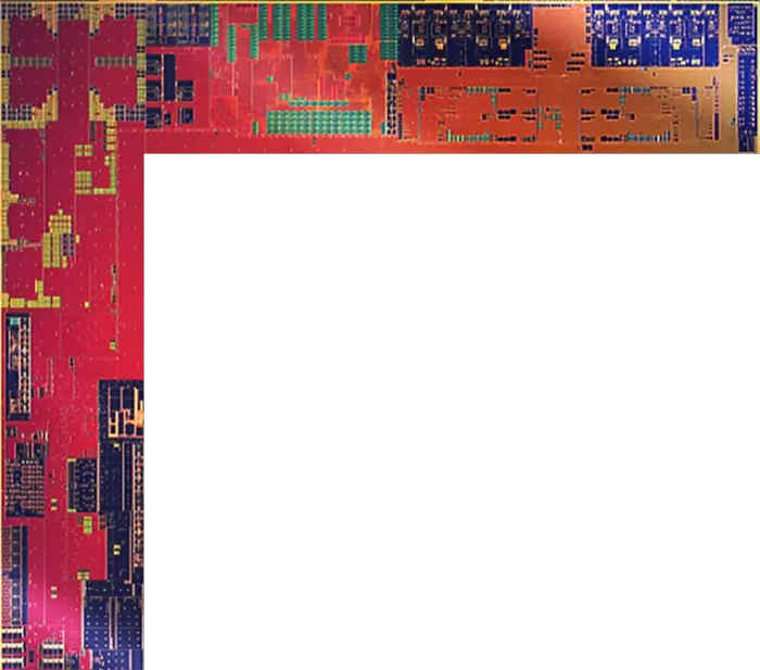
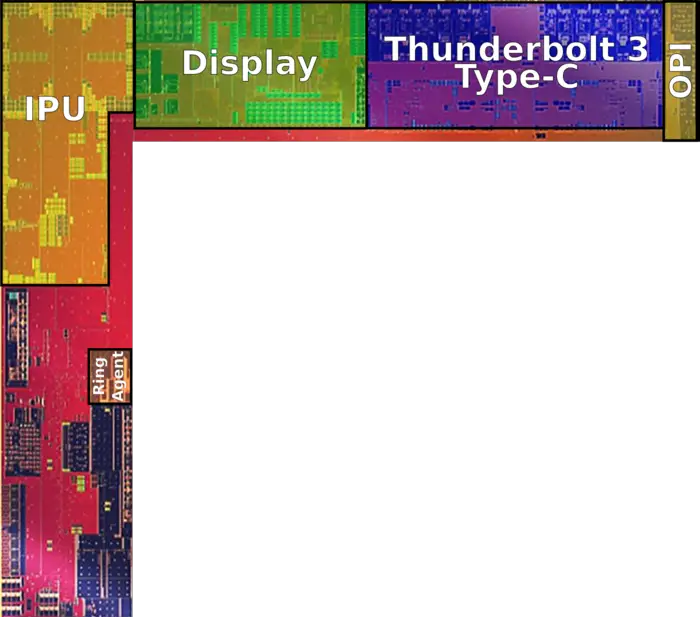
| Line 154: | Line 316: | ||
** 4th Gen IPU | ** 4th Gen IPU | ||
** Gen11 Display | ** Gen11 Display | ||
| − | ** Thunderbolt 3 over Type-C | + | ** Thunderbolt 3 over Type-C I/O subsystem |
| − | |||
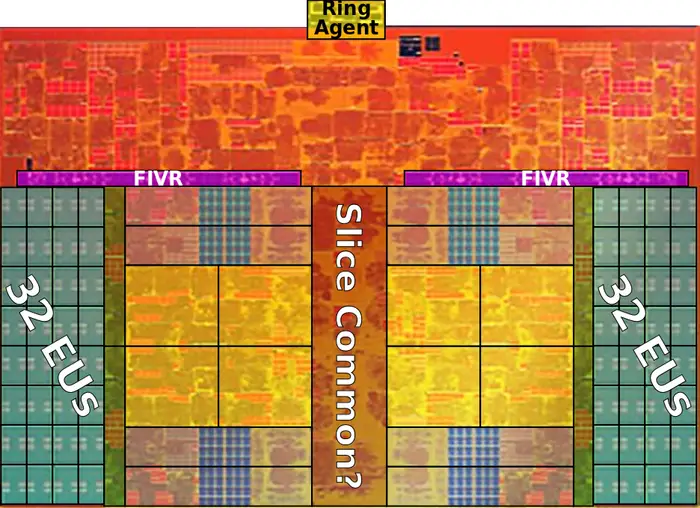
| Line 163: | Line 324: | ||
:[[File:ice lake die sa (annotated).png|700px]] | :[[File:ice lake die sa (annotated).png|700px]] | ||
| − | == | + | ==== IPU ==== |
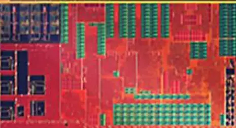
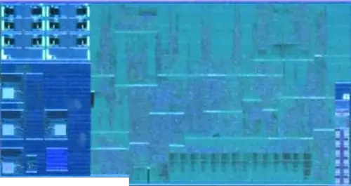
| + | :[[File:ice lake die ipu.png|500px]] | ||
| + | |||
| + | |||
| + | :[[File:ice lake die ipu 2.png|500px]] | ||
| + | |||
| + | ==== Display engine ==== | ||
| + | :[[File:ice lake die display engine.png|500px]] | ||
| + | |||
| + | |||
| + | :[[File:ice lake die display engine 2.png|500px]] | ||
| + | |||
| + | ==== Thunderbolt 3 I/O subsystem ==== | ||
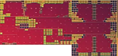
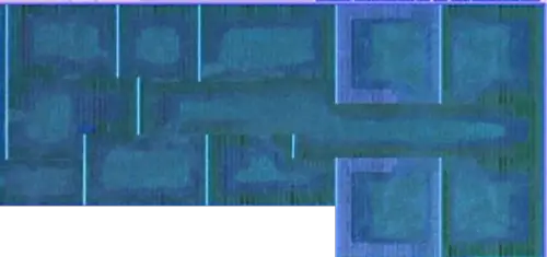
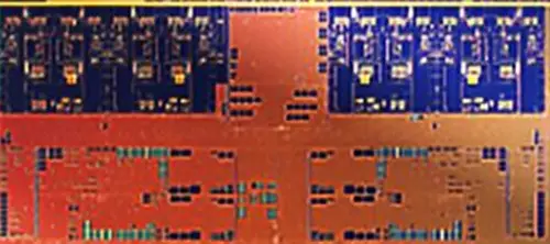
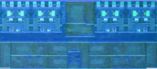
| + | :[[File:ice lake die tb3 io subsystem.png|500px]] | ||
| + | |||
| + | |||
| + | :[[File:ice lake die tb3 io subsystem 2.png|500px]] | ||
| + | |||
=== Core === | === Core === | ||
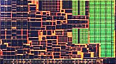
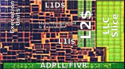
{{see also|intel/microarchitectures/sunny_cove#Die|l1=Sunny Cove § Die}} | {{see also|intel/microarchitectures/sunny_cove#Die|l1=Sunny Cove § Die}} | ||
| Line 173: | Line 351: | ||
:[[File:ice lake die core (annotated).png|400px]] | :[[File:ice lake die core (annotated).png|400px]] | ||
| + | |||
| + | |||
| + | :[[File:ice lake die core 2.png|500px]] | ||
=== Core group === | === Core group === | ||
| Line 184: | Line 365: | ||
:[[File:ice lake die core group (annotated).png|700px]] | :[[File:ice lake die core group (annotated).png|700px]] | ||
| + | |||
| + | |||
| + | :[[File:ice lake die core group 2.png|700px]] | ||
| Line 195: | Line 379: | ||
:[[File:ice lake die gpu (annotated).png|700px]] | :[[File:ice lake die gpu (annotated).png|700px]] | ||
| + | |||
| + | |||
| + | :[[File:ice lake die gpu 2.png|800px]] | ||
=== SoC === | === SoC === | ||
| Line 205: | Line 392: | ||
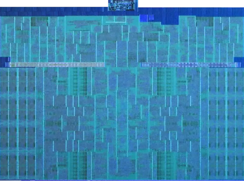
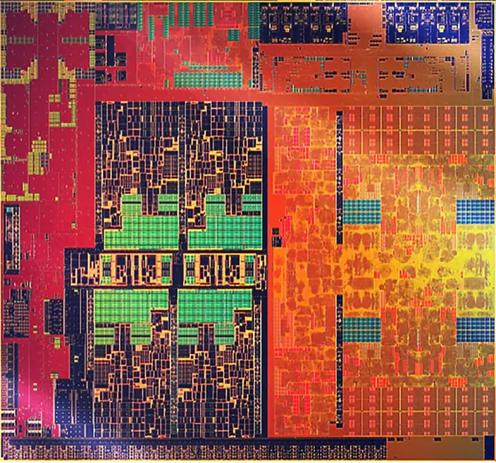
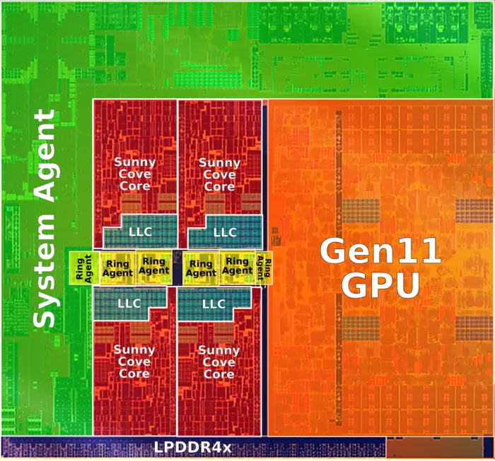
| − | :[[File:ice lake die (quad core).png|700px]] | + | :[[File:ice lake die (quad core).png|class=wikichip_ogimage|700px]] |
:[[File:ice lake die (quad core) (annotated).png|700px]] | :[[File:ice lake die (quad core) (annotated).png|700px]] | ||
| + | |||
| + | |||
| + | :[[File:ice lake die.png|800px]] | ||
| + | |||
| + | === PCH === | ||
| + | * [[14 nm process]] | ||
| + | * ~53.76 mm² die size | ||
| + | ** ~5.69 mm x 9.45 mm | ||
| + | |||
| + | |||
| + | :[[File:ice lake pch die.png|700px]] | ||
== All Ice Lake Chips == | == All Ice Lake Chips == | ||
| − | |||
| − | |||
<!-- NOTE: | <!-- NOTE: | ||
This table is generated automatically from the data in the actual articles. | This table is generated automatically from the data in the actual articles. | ||
| Line 221: | Line 417: | ||
--> | --> | ||
{{comp table start}} | {{comp table start}} | ||
| − | <table class="comptable sortable tc7 tc8 tc20 | + | <table class="comptable sortable tc7 tc8 tc19 tc20"> |
| − | {{comp table header|main| | + | {{comp table header|main|19:List of Ice Lake-based Processors}} |
| − | {{comp table header|main|10:Main processor| | + | {{comp table header|main|10:Main processor|3:{{intel|Turbo Boost}}|Memory|3:GPU}} |
| − | {{comp table header|cols|Launched|Price|Family|Platform|Core|Cores|Threads|L3$|TDP|Base|1 Core|2 Cores|4 | + | {{comp table header|cols|Launched|Price|Family|Platform|Core|Cores|Threads|L3$|TDP|Base|1 Core|2 Cores|4 Cores|Max Memory|Name|Base|Burst}} |
| − | {{#ask: [[Category:microprocessor models by intel]] [[microarchitecture::Ice Lake]] | + | {{#ask: [[Category:microprocessor models by intel]] [[microarchitecture::Ice Lake (Client)]] |
|?full page name | |?full page name | ||
|?model number | |?model number | ||
| Line 241: | Line 437: | ||
|?turbo frequency (2 cores)#GHz | |?turbo frequency (2 cores)#GHz | ||
|?turbo frequency (4 cores)#GHz | |?turbo frequency (4 cores)#GHz | ||
| − | |||
|?max memory#GiB | |?max memory#GiB | ||
|?integrated gpu | |?integrated gpu | ||
|?integrated gpu base frequency | |?integrated gpu base frequency | ||
|?integrated gpu max frequency | |?integrated gpu max frequency | ||
| − | |||
| − | |||
|format=template | |format=template | ||
|template=proc table 3 | |template=proc table 3 | ||
| − | |userparam= | + | |userparam=19 |
|mainlabel=- | |mainlabel=- | ||
}} | }} | ||
| − | {{comp table count|ask=[[Category:microprocessor models by intel]] [[microarchitecture::Ice Lake]]}} | + | {{comp table count|ask=[[Category:microprocessor models by intel]] [[microarchitecture::Ice Lake (Client)]]}} |
</table> | </table> | ||
{{comp table end}} | {{comp table end}} | ||
Latest revision as of 11:31, 20 June 2021
| Edit Values | |
| Ice Lake (client) µarch | |
| General Info | |
| Arch Type | CPU |
| Designer | Intel |
| Manufacturer | Intel |
| Introduction | May 27, 2019 |
| Process | 10 nm |
| Core Configs | 2, 4 |
| Pipeline | |
| Type | Superscalar |
| OoOE | Yes |
| Speculative | Yes |
| Reg Renaming | Yes |
| Stages | 14-19 |
| Decode | 5-way |
| Instructions | |
| ISA | x86-64 |
| Extensions | MOVBE, MMX, SSE, SSE2, SSE3, SSSE3, SSE4.1, SSE4.2, POPCNT, AVX, AVX2, AES, PCLMUL, FSGSBASE, RDRND, FMA3, F16C, BMI, BMI2, VT-x, VT-d, TXT, TSX, RDSEED, ADCX, PREFETCHW, CLFLUSHOPT, XSAVE, SGX, MPX, AVX-512 |
| Cache | |
| L1I Cache | 32 KiB/core 8-way set associative |
| L1D Cache | 48 KiB/core 12-way set associative |
| L2 Cache | 512 KiB/core 8-way set associative |
| L3 Cache | 2 MiB/core 16-way set associative |
| Cores | |
| Core Names | Ice Lake Y, Ice Lake U |
| Succession | |
| Contemporary | |
| Ice Lake (server) | |
Ice Lake (ICL) Client Configuration is Intel's successor to Cannon Lake, a 10 nm microarchitecture for mainstream mobile devices.
For mobile devices, Ice Lake is branded as 10th Generation Core i3, i5, and i7 processors.
Contents
Codenames[edit]
| Core | Abbrev | Description | Graphics | Target |
|---|---|---|---|---|
| Ice Lake Y | ICL-Y | Extremely low power | 2-in-1s detachable, tablets, and computer sticks | |
| Ice Lake U | ICL-U | Ultra-low Power | Light notebooks, portable All-in-Ones (AiOs), Minis, and conference room | |
| Ice Lake H | ICL-H | High-performance Graphics | Ultimate mobile performance, mobile workstations | |
| |
|
|
|
Lead[edit]
- Ophir Edlis - Senior Principal Engineer & Lead Architect Ice Lake SoC
Process Technology[edit]
- Main article: Intel's 10-nanometer process
Prolong delays with Intel's 10-nanometer process due to yield issues meant the terminology around that process was changed over time. Ice Lake is fabricated on Intel's second-generation enhanced 10 nm process. Originally the process was meant to succeed first-generation which was used for Cannon Lake. Unfortunately due to yield and performance reasons, Intel re-designated 2nd-generation as 1st-generation (ignoring Cannon Lake), hence the plain name of "10nm" (without any pluses).
Intel says that Ice Lake is built on their learnings from their Cannon Lake chip which were largely treated as a learning vehicle. Between Cannon Lake and Ice Lake, a number of changes were made in order to improve the process for their products. One such change was the addition of an extra metal layer (originally said to be 12, is now presumably 13 on Ice Lake) in order to improve the power delivery of the chip. Additionally, they have improved the threshold voltage of the transistors as well as their MIM cap among other changes.
Compiler support[edit]
Support for Ice Lake was added in LLVM Clang 6.0 and GCC 8.0.
| Compiler | Arch-Specific | Arch-Favorable |
|---|---|---|
| ICC | -march=icelake |
-mtune=icelake
|
| GCC | -march=icelake |
-mtune=icelake
|
| LLVM | -march=icelake |
-mtune=icelake
|
| Visual Studio | /? |
/tune:?
|
CPUID[edit]
| Core | Extended Family |
Family | Extended Model |
Model |
|---|---|---|---|---|
| U, Y | 0 | 0x6 | 0x7 | 0xE |
| Family 6 Model 126 | ||||
| ? | 0 | 0x6 | ? | ? |
| Family 6 Model ? | ||||
Architecture[edit]
Ice Lake comprises of Sunny Cove cores on the ring interconnect architecture along with Gen11 GPU, and an improved System Agent with a new display engine and I/O.
Key changes from Cannon Lake/Skylake[edit]
- Enhanced "10nm+" (from "10nm", 2nd gen)
- Core
- Sunny Cove core (from Palm Cove)
- See Sunny Cove for microarchitectural details and changes
- Sunny Cove core (from Palm Cove)
- Memory
- Graphics
- Display
- Gen 11.5 (from Gen9/Gen9.5)
- DisplayPort 1.4a with Display Stream Compression(DSC) (from DisplayPort 1.2)
- HDMI 2.0b (from HDMI 1.4)
- IPU
- 4th Gen IPU (from 3rd Gen in Skylake)
- More cameras support
- New concurrent image pipeline
- on-die MIPI interface
- New Integration
- New Gaussian Neural Accelerator 1.0 (Added in Cannon Lake but unclear to what extent)
- I/O
- Thunderbolt 3 over Type-C
- Package
- New Type3, Type4 packages
- New thin-film magnetic inductors
- 100μm copper pillars (from 130μm on 14 nm)
- New Type3, Type4 packages
This list is incomplete; you can help by expanding it.
New instructions[edit]
- See also: Sunny Cove § New Instructions
Ice Lake introduced a number of new instructions.
-
SHA- Hardware acceleration for SHA hashing operations -
CLWB- Force cache line write-back without flush -
RDPID- Read Processor ID -
AVX-512(originally introduced in Skylake (Server) but only now in client) - Additional AVX-512 extensions:
-
AVX512VPOPCNTDQ- AVX-512 Vector Population Count Doubleword and Quadword -
AVX512VNNI- AVX-512 Vector Neural Network Instructions -
AVX512GFNI- AVX-512 Galois Field New Instructions -
AVX512VAES- AVX-512 Vector AES -
AVX512VBMI2- AVX-512 Vector Bit Manipulation, Version 2 -
AVX512BITALG- AVX-512 Bit Algorithms -
AVX512VPCLMULQDQ- AVX-512 Vector Vector Carry-less Multiply
-
-
SSE_GFNI- SSE-based Galois Field New Instructions -
AVX_GFNI- AVX-based Galois Field New Instructions - Split Lock Detection - detection and cause an exception for split locks
- Fast Short REP MOV
Block Diagram[edit]
Entire SoC Overview[edit]
Individual Core[edit]
See Sunny Cove § Block Diagram.
Gen11 Graphics[edit]
See Gen11 Graphics § Block Diagram.
Overview[edit]
The Ice Lake system on a chip is a 10-nanometer SoC that is aimed at the mainstream to premium mobile and the thin-and-light market. The microprocessor consists of five major components: CPU cores, LLC, ring interconnect, system agent, and Gen11 graphics. While a lot of what Ice Lake provides is inherited from the prior generations, Intel claims that every IP on Ice Lake has been enhanced in one way or another. A major enhancement in Ice Lake over the prior generation is the integration of up to four Sunny Cove cores which provide a significant uplift in IPC. Those cores also bring AVX-512 support for the client market. Those cores, along with the system agent and the GPU, are linked over Intel's ring interconnect. The chip is fed through a new integrated memory controller that supports quad-channel 32-bit LPDDR4X memory, providing bandwidths in the range of 50-60 GB/s. Ice Lake has a new integrated GPU which is based on their Gen11 microarchitecture which provides a large improvement in graphics performance.
The system architecture in Ice Lake has been redesigned. Intel added a new Gaussian Neural Accelerator (GNA) for the acceleration of inference applications. There is a new 4th-generation image processing unit (IPU). Ice Lake integrates the entire Thunderbolt 3 I/O subsystem on-die, significantly simplifying support at the system level. Ice Lake has four Thunderbolt 3 ports. All four ports have the same capabilities and can be used simultaneously at full performance at up to 40 Gbps per port. Intel also upgraded the display engine to Gen11 with an improved display pipe that has a new Adaptive Sync and HDR-capable display pipes that support HDR 3 and DisplayPort 1.4, supporting error correction and compression.
Ice Lake chips integrate the PCH die on-package communicating over the on-package interconnect (OPI). The new PCH The PCH has an expanded I/O support for PCIe, USB, SATA, as well as audio DSP for load power voice processing. It also integrates WiFi 6+ CNVi.
On the platform level, there is a new integrated power delivery (FIVR) on both the PCH and the CPU which Intel says allows them to save on platform area by about 15% and it reduces the power delivery rails for the OEMs by roughly half.
Core[edit]
| This section is empty; you can help add the missing info by editing this page. |
Integration[edit]
Ice Lake integrates a number of additional components:
- 4th Generation image processing unit
- A new GNA neural processor
- A new Thunderbolt I/O subsystem
GNA[edit]
Ice Lake introduced a new low-power neural processor called the Gaussian Neural Accelerator v1.0 (GNA) which is integrated on the SoC and runs at very low power even when the GPU and CPUs are turned off. The GNA can be used for long-running tasks (e.g., real-time meeting transcription). The GNA can operate while the remaining parts of the SoC are in idle in order to have minimal impact on performance.
IPU[edit]
Ice Lake incorporates 4th generation image processing unit (IPU). The IPU was first introduced with Skylake mobile SoCs (note that those were 3rd gen). The 4th Gen IPU found in Ice Lake introduces a number of new enhancements. It introduces new support for 4K video capture at 30fps. There is also new hardware support for better de-noising which supports up to 16 megapixels stills in low light conditions. In addition for support more camera simultaneously, the IPU incorporates a new concurrent image pipeline, supporting multiple different processing from the same camera stream, allowing a single camera to take the functionality of multiple sensors. A common example of that is devices with both IR and RGB cameras in the laptop bezel which can now be changed to a single camera. Intel says they are exposing more registers from the IPU to software in order to provide more flexibility for applications that make use of that for machine learning. It’s also worth noting that Intel integrated the MIPI interface onto the processor as well. Previously that was found on the chipset. The change significantly improves the latency, a required attribute needed for more advanced ML-specific applications. Some of those changes are designed to form the foundation for future generations of improvements.
Thunderbolt IO subsystem[edit]
By far the largest new integration in Ice Lake is the Thunderbolt I/O Subsystem. According to Intel, this is the largest integration they have done since the integration of the graphics processing unit in Sandy Bridge. When Ice Lake was introduced, Thunderbolt 3 was the fastest and most versatile connector that was available. Not only is it four times faster than USB 3.1, but it also supports additional peripherals over PCIe, USB 3.1, and DisplayPort, though note that only PCIe and DisplayPort tunnel over Thunderbolt while the USB 3.1 is MUXed over them for direct USB support.
Ice Lake contains two modular FIAs, each one connect to a pair of Type-C ports for a total of four ports. The FIA can multiplex between a standard USB Type-C connector and a Thunderbolt connector. When serving USB 3.1, the FIA can serve as a standard USB Type-C connection, while when using PCIe/DP, it tunnels over Thunderbolt alternate mode. Each FIA is connected to the USB controller, Display Engine, and the CIO Router. The CIO Router is the actual Thunderbolt router and it can be thought of as a display engine as well. Ice Lake has a total of four PCIe controllers coming from four root complexes. Two PCIe controllers go to each of the CIOs. Previously, there was just a single PCIe controller going to the Titan Ridge controller, so there was effectively one PCIe controller for both ports. Compared to the prior generation, each port now effectively has double the bandwidth.
Previously (e.g., with Whiskey Lake), for OEMs to support Thunderbolt 3 in mobile devices, they had to use Intel's Titan Ridge controller. Titan Ridge was a discrete Thunderbolt 3 chip that came with either one or two dedicated Thunderbolt 3 ports. In order to support everything that was necessary (e.g., legacy USB 2 as well as high speed PCIe Gen 3), the controller was connected to both the CPU and the chipset. The chipset was connected over four PCIe Gen 3 lanes. The CPU had two DisplayPort connections. Each of those passed over four PCIe Gen 3 lanes. In order to offer legacy I/O support, a direct USB 2.0 link from the PCH went to the port. For charging capabilities, the port was also connected directly to a Power Deliver (PD) controller. In total, 17 PCIe Gen 3 lanes operating at around 8 GT/s were required between the Titan Ridge controller and the chipset and CPU.
Due to the design complexity introduced by the discrete controller, most mobile devices that made use of Titan Ridge only supported it on one side of the device - typically on the side of the device closer to the controller itself.
With Ice Lake, Intel simplified the overall design considerably. The biggest change comes from the fact that most of the Titan Ridge logic has been integrated into the Ice Lake SoC itself, reducing board space, routing, and the overall bill of materials. Instead of the seventeen lanes that were required by the Titan Ridge controller, Ice Lake exposes just eight lanes – four lanes to each retimer which drive the signals to the connectors. Therefore, in total there are just eight lanes operating at 20 GT/s instead of seventeen lanes operating at 8 GT/s (note that number includes the 8.1 GT/s DP links). The reduction of lanes, along with their associated components such as the buffers, reduces the overall power consumption of the system. Intel stated that, depending on the exact device design, they saw a reduction of up to 300 mW per port when the port was fully utilized. Previously, the dual-port Titan Ridge controller had a TDP of up to 2.4 W, so the overall saving is fairly sizable. The additional power saving thus translates to better performance as more of the overall power budget can be allocated for the GPU and CPU instead of the I/O.
One of the other benefits of the Thunderbolt 3 integration is that half of the lanes can be exposed to each side of the device. With the Titan Ridge controller, offering Type-C ports on the side further from the controller was more complex and was quite rare and most OEMs simply opted to offer a legacy connector of some sort such as a USB 2.0 on that side. With Ice Lake, the direct Thunderbolt lanes that go to each retimer are easily exposed to both sides of the device, meaning, at least in theory, OEMs should have no problem offering symmetrical connections on both sides of the device.
Like Titan Ridge, each retimer supports two ports. The retimers themselves are still only sold by Intel but they are a fraction of the size, so there is also a modest board space saving advantage as well. Therefore, actually, the diagram above is almost identical when offering support for up to four Thunderbolt 3 ports, twice as many as most Titan Ridge-based designs. For full support, those additional ports just need a new dedicated USB 2 connection to the PCH, and in order to also offer charging capabilities through that port, you also need a PD controller. Premium-design laptop should, therefore, be able to have up to four Thunderbolt ports – each supporting everything from power delivery to the legacy I/O to the latest high-speed interfaces such as DisplayPort and USB 3.1.
Full configuration with four ports and every feature through every port
Clock domains[edit]
Ice Lake is divided into a number of clock domains, each controlling the clock frequency of their respective unit in the processor. All clock domains are some multiple of the [virtual] bus clock (BCLK).
- BCLK - Bus/Base Clock - The system bus interface frequency (once upon a time referred to the actual FSB speed, it now serves as only a base clock reference for all other clock domains). The base clock is 100 MHz.
- Core Clock - The frequency at which the core and the L1/L2 caches operate at. (Frequency depends on the model and is represented as a multiple of BCLK).
- Ring Clock - The frequency at which the ring interconnect and LLC operate at. Data from/to the individual cores are read/written into the L3 at a rate of 32B/cycle operating at Ring Clock frequency.
- IGP Clock - The frequency at which the integrated graphics (Gen11 GPU) operates at. Data from/to the GPU are read/written into the LLC at a rate of 64B/cycle operating at this frequency as well.
- IPU - The frequency at which the image processing unit operates at
- MemClk - Memory Clock - The frequency at which the system DRAM operates at. DRAM data is transferred at a rate of 8B/cycle operating at MemClk frequency.
Power[edit]
Dynamic Tuning 2.0[edit]
- Main article: Intel Dynamic Tuning
| This section is empty; you can help add the missing info by editing this page. |
Packaging[edit]
Ice Lake comes in two packagings.
| Package | Type3 | Type4 |
|---|---|---|
| Core | Ice Lake U | Ice Lake Y |
| TDP | 15 W | 9 W |
| Dimensions | 50 x 25 x 1.3 mm | 26.5 x 18.5 x 1.0 mm |
| Balls | 1526 balls | 1377 balls |
| Ball Pitch | 0.65 mm | 0.43 mm |
| Package (Front) |  |
|
| Package (Back) |  |
|
Thin-film magnetic inductor[edit]
The new Ice Lake packages include a thin-film magnetic inductor array on the landing side. Those are said to have higher efficiency at lower power but also support the fully processor dynamic frequency range. They can be distinctly seen on the back of the chip.
Die[edit]
System Agent[edit]
- System Agent
- 4th Gen IPU
- Gen11 Display
- Thunderbolt 3 over Type-C I/O subsystem
IPU[edit]
Display engine[edit]
Thunderbolt 3 I/O subsystem[edit]
Core[edit]
- See also: Sunny Cove § Die
- ~6.91 mm² die size
- ~3.5 mm x ~1.97 mm
Core group[edit]
- See also: Sunny Cove § Die
- ~30.73 mm² die size
- ~7.86 mm x ~3.91 mm
Integrated graphics[edit]
- Gen11 GPU
- 64 EUs
- ~41.1 mm² silicon area
- ~5.22 mm x ~7.86 mm
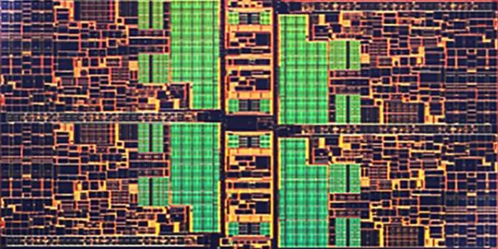
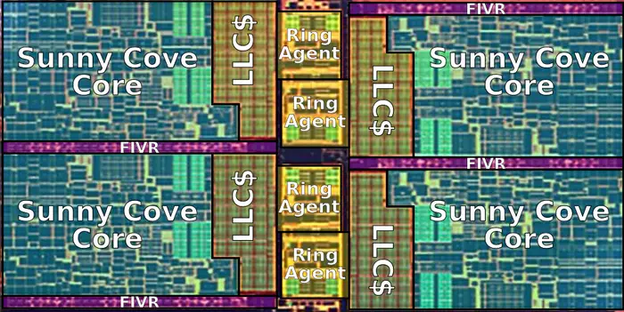
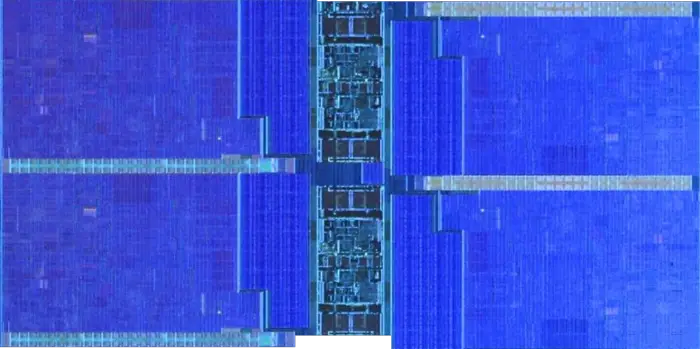
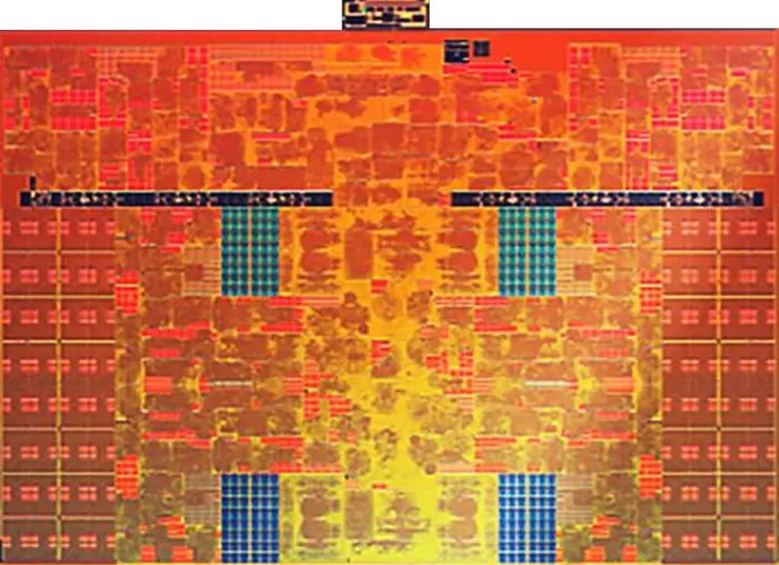
SoC[edit]
- 10 nm process
- ~122.52 mm² die size
- ~11.44 mm x ~10.71 mm
- 4 Sunny Cove big cores
- 64-EU Gen11 GPU
- 4th Gen IPU
PCH[edit]
- 14 nm process
- ~53.76 mm² die size
- ~5.69 mm x 9.45 mm
All Ice Lake Chips[edit]
| List of Ice Lake-based Processors | |||||||||||||||||||
|---|---|---|---|---|---|---|---|---|---|---|---|---|---|---|---|---|---|---|---|
| Main processor | Turbo Boost | Memory | GPU | ||||||||||||||||
| Model | Launched | Price | Family | Platform | Core | Cores | Threads | L3$ | TDP | Base | 1 Core | 2 Cores | 4 Cores | Max Memory | Name | Base | Burst | ||
| i3-1000G1 | 1 August 2019 | Core i3 | Ice Lake | Ice Lake Y | 2 | 4 | 4 MiB 4,096 KiB 4,194,304 B 0.00391 GiB | 9 W 9,000 mW 0.0121 hp 0.009 kW | 1.1 GHz 1,100 MHz 1,100,000 kHz | 3.2 GHz 3,200 MHz 3,200,000 kHz | 3.2 GHz 3,200 MHz 3,200,000 kHz | 32 GiB 32,768 MiB 33,554,432 KiB 34,359,738,368 B 0.0313 TiB | UHD Graphics | 300 MHz 0.3 GHz 300,000 KHz | 900 MHz 0.9 GHz 900,000 KHz | ||||
| i3-1000G4 | 1 August 2019 | Core i3 | Ice Lake | Ice Lake Y | 2 | 4 | 4 MiB 4,096 KiB 4,194,304 B 0.00391 GiB | 9 W 9,000 mW 0.0121 hp 0.009 kW | 1.1 GHz 1,100 MHz 1,100,000 kHz | 3.2 GHz 3,200 MHz 3,200,000 kHz | 3.2 GHz 3,200 MHz 3,200,000 kHz | 32 GiB 32,768 MiB 33,554,432 KiB 34,359,738,368 B 0.0313 TiB | Iris Plus Graphics | 300 MHz 0.3 GHz 300,000 KHz | 900 MHz 0.9 GHz 900,000 KHz | ||||
| i3-1005G1 | 1 August 2019 | $ 281.00 € 252.90 £ 227.61 ¥ 29,035.73 | Core i3 | Ice Lake | Ice Lake U | 2 | 4 | 4 MiB 4,096 KiB 4,194,304 B 0.00391 GiB | 15 W 15,000 mW 0.0201 hp 0.015 kW | 1.2 GHz 1,200 MHz 1,200,000 kHz | 3.4 GHz 3,400 MHz 3,400,000 kHz | 3.4 GHz 3,400 MHz 3,400,000 kHz | 64 GiB 65,536 MiB 67,108,864 KiB 68,719,476,736 B 0.0625 TiB | UHD Graphics | 300 MHz 0.3 GHz 300,000 KHz | 900 MHz 0.9 GHz 900,000 KHz | |||
| i5-1030G4 | 1 August 2019 | Core i5 | Ice Lake | Ice Lake Y | 4 | 8 | 6 MiB 6,144 KiB 6,291,456 B 0.00586 GiB | 9 W 9,000 mW 0.0121 hp 0.009 kW | 0.7 GHz 700 MHz 700,000 kHz | 3.5 GHz 3,500 MHz 3,500,000 kHz | 3.2 GHz 3,200 MHz 3,200,000 kHz | 32 GiB 32,768 MiB 33,554,432 KiB 34,359,738,368 B 0.0313 TiB | Iris Plus Graphics | 300 MHz 0.3 GHz 300,000 KHz | 1,050 MHz 1.05 GHz 1,050,000 KHz | ||||
| i5-1030G7 | 1 August 2019 | Core i5 | Ice Lake | Ice Lake Y | 4 | 8 | 6 MiB 6,144 KiB 6,291,456 B 0.00586 GiB | 9 W 9,000 mW 0.0121 hp 0.009 kW | 0.8 GHz 800 MHz 800,000 kHz | 3.5 GHz 3,500 MHz 3,500,000 kHz | 3.2 GHz 3,200 MHz 3,200,000 kHz | 32 GiB 32,768 MiB 33,554,432 KiB 34,359,738,368 B 0.0313 TiB | Iris Plus Graphics | 300 MHz 0.3 GHz 300,000 KHz | 1,050 MHz 1.05 GHz 1,050,000 KHz | ||||
| i5-1035G1 | 1 August 2019 | $ 297.00 € 267.30 £ 240.57 ¥ 30,689.01 | Core i5 | Ice Lake | Ice Lake U | 4 | 8 | 6 MiB 6,144 KiB 6,291,456 B 0.00586 GiB | 15 W 15,000 mW 0.0201 hp 0.015 kW | 1 GHz 1,000 MHz 1,000,000 kHz | 3.6 GHz 3,600 MHz 3,600,000 kHz | 3.3 GHz 3,300 MHz 3,300,000 kHz | 64 GiB 65,536 MiB 67,108,864 KiB 68,719,476,736 B 0.0625 TiB | UHD Graphics | 300 MHz 0.3 GHz 300,000 KHz | 1,050 MHz 1.05 GHz 1,050,000 KHz | |||
| i5-1035G4 | 1 August 2019 | $ 320.00 € 288.00 £ 259.20 ¥ 33,065.60 | Core i5 | Ice Lake | Ice Lake U | 4 | 8 | 6 MiB 6,144 KiB 6,291,456 B 0.00586 GiB | 15 W 15,000 mW 0.0201 hp 0.015 kW | 1.1 GHz 1,100 MHz 1,100,000 kHz | 3.7 GHz 3,700 MHz 3,700,000 kHz | 3.3 GHz 3,300 MHz 3,300,000 kHz | 64 GiB 65,536 MiB 67,108,864 KiB 68,719,476,736 B 0.0625 TiB | Iris Plus Graphics | 300 MHz 0.3 GHz 300,000 KHz | 1,050 MHz 1.05 GHz 1,050,000 KHz | |||
| i5-1035G7 | 1 August 2019 | $ 309.00 € 278.10 £ 250.29 ¥ 31,928.97 | Core i5 | Ice Lake | Ice Lake U | 4 | 8 | 6 MiB 6,144 KiB 6,291,456 B 0.00586 GiB | 15 W 15,000 mW 0.0201 hp 0.015 kW | 1.2 GHz 1,200 MHz 1,200,000 kHz | 3.7 GHz 3,700 MHz 3,700,000 kHz | 3.3 GHz 3,300 MHz 3,300,000 kHz | 64 GiB 65,536 MiB 67,108,864 KiB 68,719,476,736 B 0.0625 TiB | Iris Plus Graphics | 300 MHz 0.3 GHz 300,000 KHz | 1,050 MHz 1.05 GHz 1,050,000 KHz | |||
| i7-1060G7 | 1 August 2019 | Core i7 | Ice Lake | Ice Lake Y | 4 | 8 | 8 MiB 8,192 KiB 8,388,608 B 0.00781 GiB | 9 W 9,000 mW 0.0121 hp 0.009 kW | 1 GHz 1,000 MHz 1,000,000 kHz | 3.8 GHz 3,800 MHz 3,800,000 kHz | 3.4 GHz 3,400 MHz 3,400,000 kHz | 32 GiB 32,768 MiB 33,554,432 KiB 34,359,738,368 B 0.0313 TiB | Iris Plus Graphics | 300 MHz 0.3 GHz 300,000 KHz | 1,100 MHz 1.1 GHz 1,100,000 KHz | ||||
| i7-1065G7 | 1 August 2019 | $ 426.00 € 383.40 £ 345.06 ¥ 44,018.58 | Core i7 | Ice Lake | Ice Lake U | 4 | 8 | 8 MiB 8,192 KiB 8,388,608 B 0.00781 GiB | 15 W 15,000 mW 0.0201 hp 0.015 kW | 1.3 GHz 1,300 MHz 1,300,000 kHz | 3.9 GHz 3,900 MHz 3,900,000 kHz | 3.8 GHz 3,800 MHz 3,800,000 kHz | 3.5 GHz 3,500 MHz 3,500,000 kHz | 64 GiB 65,536 MiB 67,108,864 KiB 68,719,476,736 B 0.0625 TiB | Iris Plus Graphics | 300 MHz 0.3 GHz 300,000 KHz | 1,100 MHz 1.1 GHz 1,100,000 KHz | ||
| i7-1068G7 | Core i7 | Ice Lake | Ice Lake U | 4 | 8 | 8 MiB 8,192 KiB 8,388,608 B 0.00781 GiB | 28 W 28,000 mW 0.0375 hp 0.028 kW | 2.3 GHz 2,300 MHz 2,300,000 kHz | 4.1 GHz 4,100 MHz 4,100,000 kHz | 3.6 GHz 3,600 MHz 3,600,000 kHz | 64 GiB 65,536 MiB 67,108,864 KiB 68,719,476,736 B 0.0625 TiB | Iris Plus Graphics | 300 MHz 0.3 GHz 300,000 KHz | 1,100 MHz 1.1 GHz 1,100,000 KHz | |||||
| Count: 11 | |||||||||||||||||||
Bibliography[edit]
- Intel 2018 Architecture Day.
- Intel. personal communication. 2019.
| codename | Ice Lake (client) + |
| core count | 2 + and 4 + |
| designer | Intel + |
| first launched | May 27, 2019 + |
| full page name | intel/microarchitectures/ice lake (client) + |
| instance of | microarchitecture + |
| instruction set architecture | x86-64 + |
| manufacturer | Intel + |
| microarchitecture type | CPU + |
| name | Ice Lake (client) + |
| pipeline stages (max) | 19 + |
| pipeline stages (min) | 14 + |
| process | 10 nm (0.01 μm, 1.0e-5 mm) + |

