Semiconductor & Computer Engineering
| This is the discussion page for the intel/microarchitectures/ice lake (client) page. |
|
Die size[edit]
Regarding the ~11.44 mm x ~10.71 mm die dimensions.
David, do these numbers refer to printed image including streets, printed image without streets, or to physical die dimensions (after dicing)?
What are your estimates for the remaining two of three total?
I calculated meticulously all three on my own before finding out you did it too, so I think it would be interesting to compare our findings.
Regards, AM (myname4rwt@jee-male.com) 30.05.2019
- Die estimates are for the physical diced die as can be seen from the package.
- There is a measurement for one of the PCH on the page along with a die shot.
- I did not bother with the smaller PCH or the ICL-Y parts. If you are trying to get an idea of 10nm scaling, it's very good. --David (talk) 12:53, 30 May 2019 (EDT)
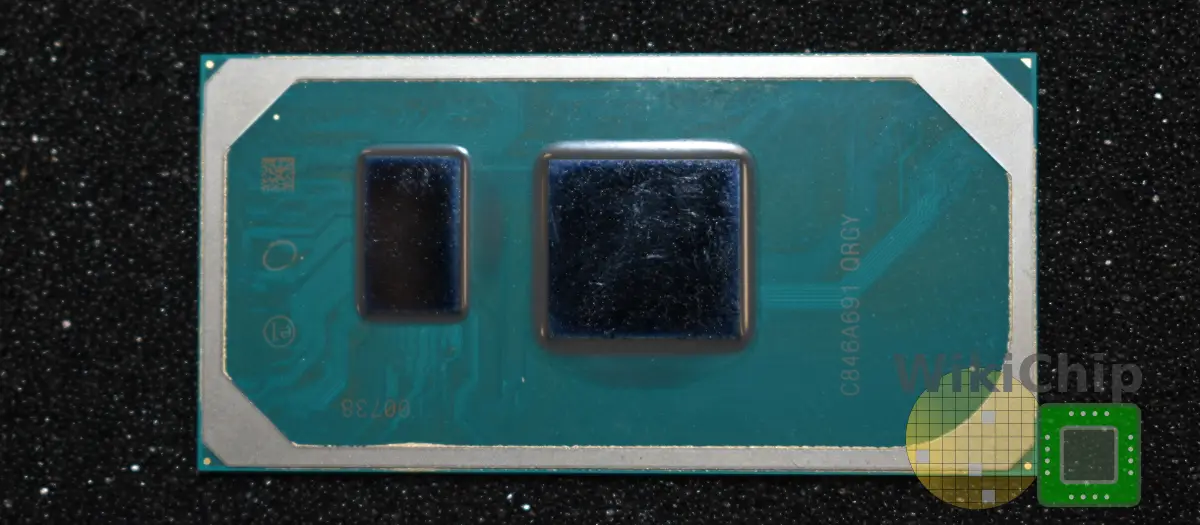
Are you talking about this photo? https://fuse.wikichip.org/wp-content/uploads/2019/05/icl-u-pkg.png
I used that photo for a quick check after my measurement and at first got 11.4 x 10.7 mm, but noticed a mistake, redid it and got 11.45 x 10.9.
Instead, I relied on wafer shots and from them my estimate for diced die is 11.7 x 10.9 -- you can't really estimate diced die dimension to the hundredth of a mm even from wafer shots because you need to know whether these wafers are stealth-diced or not, and if not, blade thickness used -- too many unknowns.
So I'm glad I got 10.9 for one dim in both cases, but concerned about the 11.45 vs 11.7 difference for the other dimension.
Time permitting, I'll redo the measurement, that's all for now.
Regards, AM (myname4rwt@jee-male.com) 30.05.2019
- Yea, similar to that picture (the actual photo is 4K res, downsized for the article) but I have a few other photos with a ruler reference. +/- 0.1 mm or so is pretty much as close as you can get on even real measurements. I have had dies I decapped that were off by close to a 0.1 mm from official die sizes... --David (talk) 15:54, 30 May 2019 (EDT)
I redid my measurements -- no mistake for wafer shots, which yield 11.78 x 10.96 = 129 mm^2 for physical die (assuming use of modern tools), but I adjusted my methodology for the package photo and got 11.54 x 10.95 -- perfect correspondence for one dimension and obvious disagreement for the other. Which bugs me.
Different steppings on wafer and package shots could explain it, but even if the stepping which went into volume production is the one on package photo (and it could well be the other way around), your measurements are slightly off -- it's quite easy to mismeasure the chip using package photo without being very meticulous about it (and it also means dimensions of units are slightly off as well). --AM (myname4rwt@jee-male.com) 30.05.2019
L1D Associativty[edit]
Does anyone know where this 12-way set associativity for the L1 data cache comes from? The Intel Ice Lake datasheet and the Intel optimization reference manual seem to indicate the L1I and L1D are both 8-way set associative caches.