(Stepping 2) |
(→Instruction set: +o) |
||
| Line 132: | Line 132: | ||
=== Instruction set === | === Instruction set === | ||
| − | The CHA SoC integrates up to eight cores, each featuring the {{x86|x86-64}} [[ISA]] along with | + | The CHA SoC integrates up to eight cores, each featuring the {{x86|x86-64}} [[ISA]] along with following {{x86|extensions}}: |
{| class="wikitable" | {| class="wikitable" | ||
Latest revision as of 03:37, 30 September 2022
| Edit Values | |
| CHA µarch | |
| General Info | |
| Arch Type | CPU |
| Designer | Centaur Technology |
| Manufacturer | TSMC |
| Process | 16 nm |
| Core Configs | 8 |
| Pipeline | |
| Type | Superscalar, Superpipeline |
| OoOE | Yes |
| Speculative | Yes |
| Reg Renaming | Yes |
| Stages | 20-22 |
| Decode | 4-way |
| Instructions | |
| ISA | x86-64 |
| Extensions | MMX, SSE, SSE2, SSE3, SSSE3, SSE4.1, SSE4.2, AVX, AVX2, AES, BMI, BMI2, AVX-512 |
| Cache | |
| L1I Cache | 32 KiB/core 8-way set associative |
| L1D Cache | 32 KiB/core 8-way set associative |
| L2 Cache | 256 KiB/core 16-way set associative |
| L3 Cache | 2 MiB/core 16-way set associative |
CHA is a 16-nanometer x86 SoC microarchitecture designed by Centaur Technology for the server market.
Contents
History[edit]
Centaur started working on CHA around the 2016 timeframe as a new ground-up x86 SoC design.
Release dates[edit]
Centaur announced the CHA SoC in late 2019. The chip is expected to launch for production in late 2020.
Process technology[edit]
CHA is designed for TSMC 16 nm process.
Compiler support[edit]
| Compiler | Arch-Specific | Arch-Favorable |
|---|---|---|
| ICC | -march=??? |
-mtune=???
|
| GCC | -march=??? |
-mtune=???
|
| LLVM | -march=??? |
-mtune=???
|
| Visual Studio | /arch:AVX512 |
/tune:???
|
CPUID[edit]
| Core | Extended Family |
Family | Extended Model |
Model | Stepping |
|---|---|---|---|---|---|
| Centaur CNS | 0 | 0x6 | 0x4 | 0x7 | 0x2 |
| Family 6 Model 71 Stepping 2 | |||||
Architecture[edit]
Key changes from CN[edit]
| This section is empty; you can help add the missing info by editing this page. |
Block Diagram[edit]
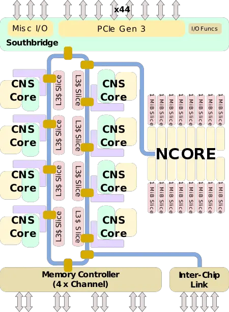
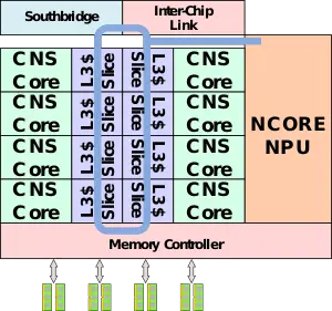
CHA SoC[edit]
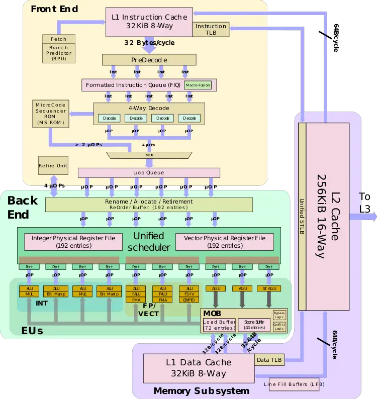
CNS Core[edit]
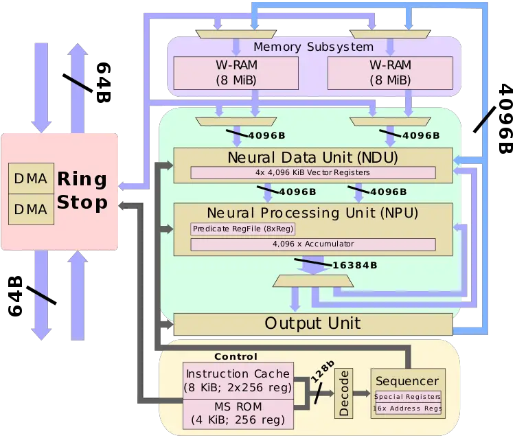
NCORE NPU[edit]
Memory Hierarchy[edit]
- Cache
- L1I Cache:
- 32 KiB, 8-way set associative
- 64 sets, 64 B line size
- 64 B/cycle bandwidth to L1$
- 32 KiB, 8-way set associative
- L1D Cache:
- 32 KiB, 8-way set associative
- 64 sets, 64 B line size
- 64 B/cycle load bandwidth
- 32-64 B/cycle store bandwidth
- 64 B/cycle bandwidth to L1$
- 4 cycles fastest load-to-use, 4-6 cycles depending on address mode
- 32 KiB, 8-way set associative
- L2 Cache:
- Unified, 256 KiB, 16-way set associative
- 256 sets, 64 B line size
- 64 B/cycle bandwidth to L1$
- 13 cycles load-to-use
- Unified, 256 KiB, 16-way set associative
- L3 Cache/LLC:
- 2 MiB Per core, shared across all cores
- Up to 16-way set associative
- 64 B line size
- Per each core:
- Read: 64 B/cycle to/fromt ring
- Write: 64 B/cycle to/fromt ring
- System DRAM:
- 8 B/cycle/channel (@ memory clock)
- 4 Channels
- DDR4, up to 3,200 MT/s
- L1I Cache:
- NCORE
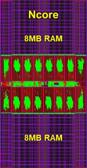
- 16 MiB SRAM
- 2x8 MiB banks (D-RAM and W-RAM)
- May be used as large scratchpad if NCORE is not used (limited to 1 x86 process at a time)
- Not coherent with L3 or DRAM
- Instruction cache
- Instruction ROM
- 4 KiB
- 256 x 128-bit instructions
- 4 KiB
- Instruction memory
- 8 KiB
- 2 banks x 256 x 128-bit instructions
- 8 KiB
- Instruction ROM
- 16 MiB SRAM
Instruction set[edit]
The CHA SoC integrates up to eight cores, each featuring the x86-64 ISA along with following extensions:
| MMX | SSE | SSE2 | SSE3 |
| SSSE3 | SSE4.1 | SSE4.2 | AES |
| AVX | AVX2 | FMA3 | SHA |
| AVX512 | |||
| AVX512F | AVX512CD | AVX512BW | AVX512DQ |
| AVX512VL | AVX512IFMA | AVX512VBMI |
Overview[edit]
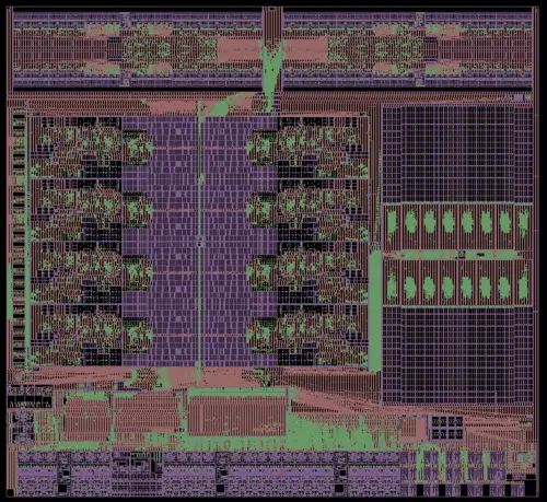
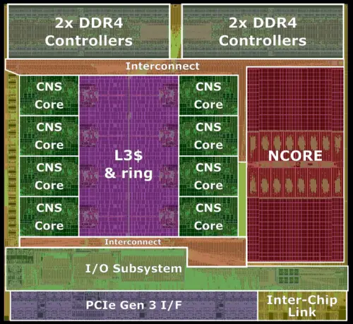
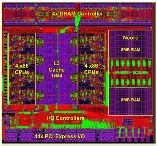
Announced in 2019 and expected to be introduced in 2020, CHA (pronounced C-H-A) is a new ground-up x86 SoC designed by Centaur for the server, edge, and AI market. Fabricated on TSMC 16 nm process, the chip integrates eight high-performance x86 "CNS" cores along with a brand new clean-sheet design "NCORE" neural processor. CHA is a fully integrated SoC. It incorporates both the source bridge and north bridge on-die. All the cores, along with the NCORE, the southbridge, and memory controller are all interconnected on a ring. The chip supports up to quad-channel DDR4 memory and up to 44 PCIe Gen 3 lanes. Likewise, the southbridge provides all the usual legacy I/O functionality. Targetting the server market as well, CHA adds the ability to directly link to a second CHA SoC in a 2-way multiprocessing configuration.
This is the first server x86 chip to integrate an AI accelerator. The CHA SoC features new CNS cores which introduce considerably higher single-thread performance over the prior designs. The cores also introduce the AVX-512 extension in order to offer better performance, flexibility, and offer better ISA compatibility with other x86 vendors such as Intel. The integrated NPU is designed to allow for a reduction of platform cost by offering an AI inference coprocessor "free" on-die along with the standard server-class x86 cores. For many workloads, the on-die specialized inference acceleration means it's no longer required to add a third-party PCIe-based accelerator card.
CNS Core[edit]
CNS is the x86 core integrated into CHA. This is a 4-way wide front-end out-of-order pipeline with an eight-wide back-end. The pipeline is relatively long with 20 stages for the integer pipeline and 22 stages for memory operations (that hit the L1D$).
Front-end[edit]
The front-end of CNS deals with the fetching of instructions, decoding, and queuing them up for execution. At a high level, Centaur significantly improved the front-end of the machine versus prior generations. The CNS core has a better branch predictor and better prefetchers.
Fetch and decode[edit]
CNS has a 32 KiB L1 instruction cache organized as 8 ways of 64 sets. Running ahead of the instruction stream, the CNS prefetchers will attempt to ensure the instruction stream is resident in that cache. Centaur has stated CNS featured improved prefetchers although no specifics were disclosed.
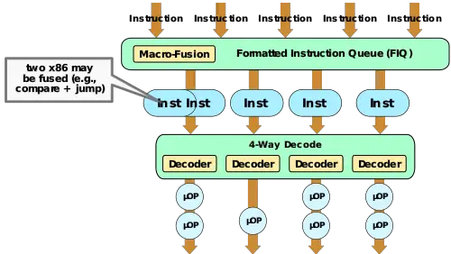
Each cycle, up to 32 bytes (half a line) of the instruction stream are fetched from the instruction cache into the instruction pre-decode queue. Since x86 instructions may range from a single byte to 15 bytes, this buffer receives an unstructured byte stream which is then marked at the instruction boundary. In addition to marking instruction boundaries, the pre-decode also does various prefix processing. From the pre-decode queue, up to five individual instructions are fed into the formatted instruction queue (FIQ).
Prior to getting sent to decode, the FIQ has the ability to do macro-op fusion. CNS can detect certain pairs of adjacent instructions such as a simple arithmetic operation followed by a conditional jump and couple them together such that they get decoded at the same time into a fused operation. This was improved further with the new CNS core.
From the FIQ, up to four instructions (or five if fused) are sent to the decode. CNS features four homogenous decoders - each capable of decoding all types of instructions. At the decode, x86 instructions are transformed into micro-operations. Most instructions will translate into a single micro-operation while more complex instructions (e.g., register-memory) will emit two µOPs. For fused instructions, those instructions are decoded into a fused micro-operations which remain fused for its remaining lifetime. In other words, those fused instructions will also retire as a fused instruction. This enables CNS to decode up to five instructions per cycle, reducing the effective bandwidth across the entire pipeline from the fused operations.
Following decode, instructions are queued up in the micro-operation queue which serves to decouple the front-end from the back-end.
Back-end[edit]
The back-end deals with the out-of-order execution of instructions. CNS introduces major improvements to the back-end over prior generations. From the front-end, micro-operations are fetched from the micro-op queue which decouples the front-end from the back-end. Each cycle, up to four instructions can be renamed (and later retire). This is an increase from the previously 3-wide rename. The widening of rename and retire match the decode rate of the front-end. Once renamed, micro-operations are sent to the scheduler. For fused operations, instructions will remain fused throughout the pipeline and will retire fused. Therefore retire has a max retirement bandwidth of 5 x86 instructions per clock.
Prior Centaur chips were manufactured on relatively older process nodes such as 65 nm and later 45 nm. The move to a more leading-edge node (TSMC 16-nanometer FinFET, in this case) provided them with a significantly higher transistor budget. Centaur takes advantage of that to build a wider out-of-order core. To that end, Centaur's CNS core supports 192 OoO instructions in-flight. This is identical to both Intel Haswell and AMD Zen.
Execution ports[edit]
Centaur employs a relatively wide unified scheduler design. CNS has ten dedicated execution ports – they are physically partitioned into three groups: integer, floating-point (and AVX), and memory. In terms of scheduler width, this is rivaling both Intel and AMD contemporary designs.
Integer[edit]
CNS integrates four integer units. Two of the units also incorporate multipliers while the other two have bit-manipulation units (BMUs). Up to two branch instructions can be executed each cycle.
Floating Point & Vector[edit]
CNS incorporates three dedicated ports for floating-point and vector operations. Two of the ports support FMA operations while the third has the divide and crypto units. All three pipes are 256-bit wide. In terms of raw compute power, the total FLOPS per core is 16 double-precision FLOPs/cycle – reaching parity with AMD Zen 2 as well as Intel's Haswell, Broadwell, and Skylake (Client).
CNS added extensive x86 ISA support, including new support for AVX-512. CNS supports all the AVX-512 extensions supported by Intel's Skylake (Server) as well as those found in Palm Cove. From an implementation point of view, Centaur's CNS cores Vector lanes are 256-wide, therefore AVX-512 operations are cracked into two 256-wide operations which are then scheduled independently. In other words, there is no throughput advantage here. The design is similar to how AMD dealt with AVX-256 in their Zen core where operations had to be executed as two 128-bit wide operations. Note that the implementation of AVX-512 on CNS usually exhibits no downclocking. The design of the core was such that it's designed to operate at the full frequency of the core and the rest of the SoC. Centaur does implement a power management engine that's capable of downclocking for certain power-sensitive SKUs if necessary.
Memory subsystem[edit]
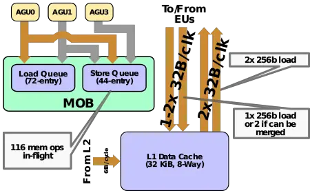
The memory subsystem on CNS features three ports - two generic AGUs and one store AGU port. In other words, two of the ports are capable of dispatching loads or store addresses and an additional port that is capable of dispatching a store address only. CNS supports 116 memory operations in-flight. The MOB consists of a 72-entry load-buffer and a 44-entry store buffer. Data store operations are done via the execution units that forward the data to the store buffer. On CNS, up to 4 values may be forwarded to store - they may be any combination of up to four integers and two media values.
CNS features a level 1 data cache with a capacity of 32 KiB. The cache is organized as 8 ways of 64 sets. It is fully multi-ported, capable of supporting 2 reads and 1 write every cycle. Each port is 32B wide, therefore 512-bit memory operations, like the arithmetic counterparts, have to be cracked into two 256-bit operations. With two load operations, CNS can do a single 512-bit operation each cycle. Note that although there is a single write port, if two 256-bit stores are consecutive stores to a single cache line, they can both be committed in a single cycle.
Lines to the L1 data cache as well as the L1 instruction cache come from the level 2 cache. Each core features a private level 2 cache with a capacity of 256 KiB which is organized as a 16-way set associative. Each cycle, up to 512 bits may be transferred from the L2 to the either of the L1 caches.
NCORE NPU[edit]
The AI accelerator coprocessor sits on the same ring as the rest of the chip with its own dedicated ring stop. NCORE has two DMA channels, each capable of reading and writing to/from the L3 cache slices, DRAM, and in theory also I/O. NCORE has a relatively different architecture to many of the dedicated neural processors developed contemporaneously by various startups. To that end, NCORE is an extremely-wide 32,768-bit (4K-byte) VLIW SIMD coprocessor. This is similar to what a hypothetical "AVX32768" extension would look like. The coprocessor is a programmable coprocessor that's capable of controlling up to 4K-lanes of logic each cycle at the same clock frequency as the CPU cores. 4K bytes operations are available every cycle and since the NCORE is directly connected to the ring, latency is extremely low compared to externally-attached accelerators.
The NCORE is single-threaded. Instructions are brought to the NCORE through the ring and are stored in a centralized instruction unit. The unit incorporates a 12 KiB instruction cache which includes a 4 KiB instruction ROM. Each cycle, a single 128-bit instruction is fetched, decoded, and gets executed by a sequencer which simultaneously controls all the compute slices and memory. The instruction ROM is used for executing validation code as well as commonly-used functions. The instruction sequencer incorporates a loop counter and various special registers along with sixteen address registers and dedicated hardware for performing on various addressing modes and auto-incrementation operations. The entire NCORE datapath is 4,096-byte wide.
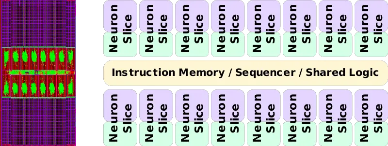
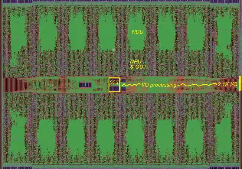
Data to the NCORE are fed into the NCORE caches. Data is fed by the two DMA channels on the ring stop interface. These DMA channels can go out to the other caches or memory asynchronously. On occasion, data may be fed from the device driver or software running on one of the CPU cores which can move instructions and data into the NCORE RAM. The NCORE features a very large and very fast (single-cycle) 16 MiB SRAM cache. The cache comprises two SRAM banks - D-RAM and W-RAM - each one is 4,096-bytes wide and is 64-bit ECC-protected. The caches are not coherent with the L3 or DRAM. Since the RAM is available even when the NCORE is not used, it may be used as a scratch path for a given process (1 process at a time). The two SRAMs operate at the same clock as the NCORE itself which is the same clock as the CPU cores. Each cycle, up to two reads (one form each bank) can be done. With each bank having a 4,096-byte interface, each cycle up to 8,192-bytes can be read into the compute interface. This enables the NCORE to have a theoretical peak read bandwidth of 20.5 TB/s. It's worth noting that physically, the NCORE is built up using small compute units called "slices" or "neurons". The design is done in this way in order to allow for future reconfigurability. The full CHA configuration features 16 slices. Each slice is a 256-byte wide SIMD unit and is accompanied by its own 2,048 256B-wide rows cache slice.
Pipeline[edit]
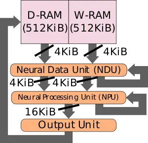
The NCORE is subdivided into four components - the caches, the neural data unit (NDU), the neural processing unit (NPU), and the output unit. The caches, NDU, and NPU are designed as single-cycle loops. The output of those units must be available as inputs to the same units on the next clock such that they can continuously operate as needed. Note that the output unit is most single-cycle as well with the exception of special output functions that might require multiple cycles to complete. Since the output functions are generally executed only once in a few million cycles, this does not normally cause any sort of stalling on the pipeline.
Neural data unit (NDU)[edit]
The compute interface passes the data from the RAMs to the neural data unit (NDU). The neural data unit operates on incoming data on each clock before it goes to the SIMD processing unit. The purpose of the data unit is to simply prepare data for the neural processing unit by doing various pre-processing. The data unit has a four-entry 4K register file which can also serve as inputs for various operations and has output to the next stage in the pipeline. Functions have eight possible inputs and four possible output registers, each 4K in size. The data unit can do operations many different operations an entire 4L-byte row in a single cycle. Operations include rotate (by 1,2,4,8,16,32,64, or -1 bytes), broadcast (taking one byte from each 64B-slice and expend it into 64 bytes for replication used in weight structuring for convolutions), merge from two inputs (e.g., RAM and register), edge swap, compress data (for pooling operations), and various other specialized functions. Under normal ML workloads, broadcast and rotate are done on almost every cycle in order to reshape the data for processing.
Neural processing unit (NPU)[edit]
Each cycle, the neural processing unit reads data out of one or two of the four registers in the neural data unit. Alternatively, input data can also be moved from one neural register to the next. This is designed to efficiently handle fully connected neural networks. The neural processing unit (NPU) does various computations such as MAC operations, shifting, min/max, and various other functions designed to add flexibility in terms of support in preparation for future AI functionalities and operations. There is also extensive support for predication with 8 predication registers. The unit is optimized for 8-bit integers (9-bit calculations) but can also operate on 16-bit integers as well as bfloat16. Wider data types allow for higher precision but they incur a latency penalty. 8-bit operations can be done in a single cycle while 16-bit integer and floating-point operations require three cycles to complete. The neural processing unit incorporates a 32-bit 4K accumulator which can operate in both 32b-integer and 32b-floating-point modes. The accumulator saturates on overflows to prevent wrap-around (e.g., the biggest positive to biggest negative). Following the millions or billions of repeated MAC operations, the output is sent to the output unit for post-processing.
| Peak Compute | |||
|---|---|---|---|
| Data Type | Int8 | Int16 | bfloat16 |
| MACs/cycle | 4,096 | 682.67 | 682.67 |
| Peak OPs | 20.5 TOPS | 3.42 TOPS | 3.42 TFLOPS |
| Frequency | 2.5 GHz | ||
Output unit[edit]
Data from the neural processing unit is sent to the output unit for post-processing. Here the unit incorporates an activation unit which can perform the standard activation functions such as sigmoid, TanH, ReLu, and others. Additionally, the output unit can perform data compression and quantization to be used in the next convolution. The output unit can do various conversions such as taking the 32b accumulator values from the processing unit and transforming them into 8-bit integers or 16-bit integer or bfloat16 values.
The output unit incorporates various other less common functionalities that run at a slightly slower rate than 4K/clock. The most complex functions are fully pipelined internally at up to 10 clocks worst case. Results form the output unit is stored into 2 out (4K) registers that can be used to write directly back to the caches or forwarded to the NDU unit as input.
On various rare occasions, some functionality might not be possible on the NCORE (e.g., an operation that's done once an image). Here, the core can use the standard x86 core to do such operations. Centaur's device driver manages the runtime stack which is capable of feeding the NCORE with NCORE instructions and operations and the x86 core with various other subroutines to execute when necessary which can take advantage of the AVX-512 support to accelerate various operations.
Communication[edit]
There are a number of ways the NCORE can be communicated with. The individual CNS cores can directly read and write to the NCORE using the virtual address space of the process (e.g., open()). AVX512 mov operations can also be used. The cores can also read the control and status registers. In turn, the NCORE can interrupt back to the core for follow-up post-processing. The two DMA controllers in the NCORE are also capable of communicating with the cache slices in the cores, the DRAM controllers, and optionally, other PCIe I/O devices.
Instructions[edit]
Instructions are 128-bit wide and execute in 1 clock cycle (including 0-cycle branches). Most instructions typically require 64-80 bits (roughly 1/2-3/4). Detailed definitions of the instructions are not made public as they are designed to be highly hardware-dependent designed for software to simplify the hardware and extract additional power efficiency. To that end, the instructions will likely change with new hardware versions.
- 30b: control of 2 RAM read & index operations
- 22b: branch control
- 20b: control of NPU
- 15b: control of NDU write to RAM
- 26b: control of NDU
- 15b: misc
Ring[edit]
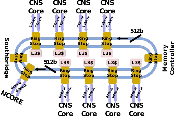
CHA interlinks all the components on the chip through a bidirectional ring interconnect. There is a dedicated ring stop for every one of the eight CNS cores. This ring stop is shared with it's corresponding L3 cache slice. There are additional ring stops for the NCORE NPU, one for the southbridge, and another one for the memory controller.
The ring itself consists of two opposing unidirectional rings. Each ring is 512-bit wide. Each cycle, a packet is passed from one ring stop to the next ring stop. The ring operates at the same clock frequency as the cores. At 2.5 GHz, the ring has a peak theoretical bandwidth of 1.28 Tb/s (160 GB/s) in each direction and a total bidirectional bandwidth of 2.56 Tb/s or 320 GB/s.
Scalability[edit]
CHA has support for two-way symmetric multiprocessing through the inter-chip link. Centaur did not disclose more information regarding the specification of the connection.
Die[edit]
SoC[edit]
- TSMC 16 nm process (16FFC)
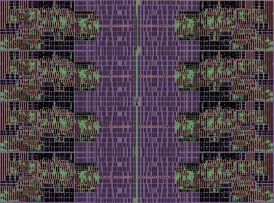
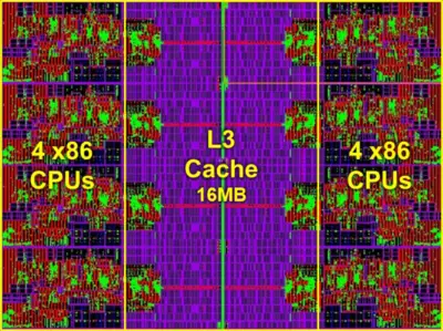
- 194 mm²
Core group[edit]
- ~63.2 mm²
CNS Core[edit]
- ~4.29 mm²
NCORE[edit]
- 32,768-bits SIMD, 16 MiB cache
- 34.4 mm² silicon area
NCORE logic[edit]
- 11 mm² silicon area
- 1.3 million regs
- 19.5 million NAND gates
Bibliography[edit]
- Centaur. personal communication. November 2019.
- Glenn Henry (Centaur). Stanford EE380 Computer Systems Colloquium. February 12, 2020.
See also[edit]
- Direct Competition
| codename | CHA + |
| core count | 8 + |
| designer | Centaur Technology + |
| full page name | centaur/microarchitectures/cha + |
| instance of | microarchitecture + |
| instruction set architecture | x86-64 + |
| manufacturer | TSMC + |
| microarchitecture type | CPU + |
| name | CHA + |
| pipeline stages (max) | 22 + |
| pipeline stages (min) | 20 + |
| process | 16 nm (0.016 μm, 1.6e-5 mm) + |
