(→All Kaby Lake Chips) |
(→Configurability) |
||
| (235 intermediate revisions by 25 users not shown) | |||
| Line 1: | Line 1: | ||
{{intel title|Kaby Lake|arch}} | {{intel title|Kaby Lake|arch}} | ||
{{microarchitecture | {{microarchitecture | ||
| − | | name | + | |atype=CPU |
| − | | designer | + | |name=Kaby Lake |
| − | | manufacturer | + | |designer=Intel |
| − | | introduction | + | |manufacturer=Intel |
| − | + | |introduction=August 30, 2016 | |
| − | | process | + | |process=14 nm |
| − | | cores | + | |cores=2 |
| − | | cores 2 | + | |cores 2=4 |
| − | + | |type=Superscalar | |
| − | + | |speculative=Yes | |
| − | + | |renaming=Yes | |
| − | + | |stages min=14 | |
| − | + | |stages max=19 | |
| − | + | |isa=x86-64 | |
| − | + | |extension=MOVBE | |
| − | + | |extension 2=MMX | |
| − | + | |extension 3=SSE | |
| − | + | |extension 4=SSE2 | |
| − | + | |extension 5=SSE3 | |
| − | | type | + | |extension 6=SSSE3 |
| − | + | |extension 7=SSE4.1 | |
| − | | speculative | + | |extension 8=SSE4.2 |
| − | | renaming | + | |extension 9=POPCNT |
| − | + | |extension 10=AVX | |
| − | + | |extension 11=AVX2 | |
| − | | stages min | + | |extension 12=AES |
| − | | stages max | + | |extension 13=PCLMUL |
| − | | | + | |extension 14=FSGSBASE |
| − | + | |extension 15=RDRND | |
| − | + | |extension 16=FMA3 | |
| − | + | |extension 17=F16C | |
| − | | extension | + | |extension 18=BMI |
| − | | extension 2 | + | |extension 19=BMI2 |
| − | | extension 3 | + | |extension 20=VT-x |
| − | | extension 4 | + | |extension 21=VT-d |
| − | | extension 5 | + | |extension 22=TXT |
| − | | extension 6 | + | |extension 23=TSX |
| − | | extension 7 | + | |extension 24=RDSEED |
| − | | extension 8 | + | |extension 25=ADCX |
| − | | extension 9 | + | |extension 26=PREFETCHW |
| − | | extension 10 | + | |extension 27=CLFLUSHOPT |
| − | | extension 11 | + | |extension 28=XSAVE |
| − | | extension 12 | + | |extension 29=SGX |
| − | | extension 13 | + | |extension 30=MPX |
| − | | extension 14 | + | |l1i=32 KiB |
| − | | extension 15 | + | |l1i per=core |
| − | | extension 16 | + | |l1i desc=8-way set associative |
| − | | extension 17 | + | |l1d=32 KiB |
| − | | extension 18 | + | |l1d per=core |
| − | | extension 19 | + | |l1d desc=8-way set associative |
| − | | extension 20 | + | |l2=256 KiB |
| − | | extension 21 | + | |l2 per=core |
| − | | extension 22 | + | |l2 desc=4-way set associative |
| − | | extension 23 | + | |l3=2 MiB |
| − | | extension 24 | + | |l3 per=core |
| − | | extension 25 | + | |l3 desc=Up to 16-way set associative |
| − | | extension 26 | + | |side cache=64 MiB |
| − | | extension 27 | + | |side cache per=package |
| − | | extension 28 | + | |side cache desc=on Iris Plus GPUs only |
| − | | extension 29 | + | |core name=Kaby Lake Y |
| − | | extension 30 | + | |core name 2=Kaby Lake U |
| − | + | |core name 3=Kaby Lake R | |
| − | + | |core name 4=Kaby Lake H | |
| − | + | |core name 5=Kaby Lake G | |
| − | | l1i | + | |core name 6=Kaby Lake S |
| − | | l1i per | + | |core name 7=Kaby Lake DT |
| − | | l1i desc | + | |core name 8=Kaby Lake X |
| − | | l1d | + | |predecessor=Skylake |
| − | | l1d per | + | |predecessor link=intel/microarchitectures/skylake |
| − | | l1d desc | + | |successor=Coffee Lake |
| − | | l2 | + | |successor link=intel/microarchitectures/coffee lake |
| − | | l2 per | + | |successor 2=Cannon Lake |
| − | | l2 desc | + | |successor 2 link=intel/microarchitectures/cannon lake |
| − | | l3 | ||
| − | | l3 per | ||
| − | | l3 desc | ||
| − | | | ||
| − | | | ||
| − | | | ||
| − | |||
| − | |||
| − | | core name | ||
| − | | core name 2 | ||
| − | | core name 3 | ||
| − | | core name 4 | ||
| − | | core name 5 | ||
| − | | core name 6 | ||
| − | |||
| − | | | ||
| − | | predecessor | ||
| − | | predecessor link = intel/microarchitectures/skylake | ||
| − | | successor | ||
| − | | successor link | ||
| − | | successor 2 | ||
| − | | successor 2 link = intel/microarchitectures/ | ||
}} | }} | ||
| − | [[File:7th Gen Core-i7-badge.png|thumb|right| | + | [[File:7th Gen Core-i7-badge.png|thumb|right|175px|Kaby Lake is Intel's 7th Generation {{intel|Core i7}} MPUs.]] |
| − | '''Kaby Lake''' ('''KBL''') is [[Intel]]'s successor to {{\\|Skylake}}, an enhanced [[14 nm process]] [[microarchitecture]] for mainstream desktops | + | '''Kaby Lake''' ('''KBL''') is [[Intel]]'s successor to {{\\|Skylake}}, an enhanced [[14 nm process]] [[microarchitecture]] for mainstream desktops and mobile devices. Kaby Lake is the first "Optimization" released as part of Intel's {{intel|PAO}} model. The microarchitecture was developed by Intel's R&D center in [[wikipedia:Haifa, Israel|Haifa, Israel]]. {{\\|Cannon Lake}} was originally set to replace {{\\|Skylake}} as the next microarchitecture using a [[10 nm process]], however Intel later revised their roadmap to include Kaby Lake (with Cannon Lake being pushed back to [[2018]]). |
| − | For desktop and mobile, Kaby Lake is branded as 7th Generation Intel {{intel|Core i3}}, {{intel|Core i5}}. and {{intel|Core i7}} processors. For | + | For desktop and mobile, Kaby Lake is branded as 7th Generation Intel {{intel|Core i3}}, {{intel|Core i5}}. and {{intel|Core i7}} processors. For workstation class processors, Intel branded it as {{intel|Xeon E3|Xeon E3 v6}}. There are no Kaby Lake-based server microprocessors. |
== Codenames == | == Codenames == | ||
{| class="wikitable" | {| class="wikitable" | ||
|- | |- | ||
| − | ! Core !! Abbrev !! Description !! Graphics !! Target | + | ! Core !! Abbrev !! Platform || Description !! Graphics !! Target |
| + | |- | ||
| + | | {{intel|Kaby Lake Y|l=core}} || KBL-Y || || Extremely low power || GT2 || 2-in-1s detachable, tablets, and computer sticks | ||
| + | |- | ||
| + | | {{intel|Kaby Lake U|l=core}} || KBL-U || || Ultra-low Power || GT2/GT3 || Light notebooks, portable All-in-Ones (AiOs), Minis, and conference room | ||
|- | |- | ||
| − | | Kaby Lake | + | | {{intel|Kaby Lake R|l=core}} || KBL-R || || Ultra-low Power || GT2 || Kaby Lake U Refresh |
|- | |- | ||
| − | | Kaby Lake | + | | {{intel|Kaby Lake H|l=core}} || KBL-H || || High-performance Graphics || GT2/GT3 || Ultimate mobile performance, mobile workstations |
|- | |- | ||
| − | | Kaby Lake | + | | {{intel|Kaby Lake S|l=core}} || KBL-S || || Performance-optimized lifestyle || GT2/GT3 || Desktop performance to value, AiOs, and minis |
|- | |- | ||
| − | | Kaby Lake | + | | {{intel|Kaby Lake G|l=core}} || KBL-G || {{intel|Pedlow|l=platform}} || Gaming Chip || GT2 + AMD {{amd|Vega|l=arch}} || Kaby Lake + Radeon Vega 20/24 |
|- | |- | ||
| − | | Kaby Lake X || KBL-X || Extreme Performance || || High-end desktops & enthusiasts market | + | | {{intel|Kaby Lake X|l=core}} || KBL-X || {{intel|Basin Falls|l=platform}} || Extreme Performance || || High-end desktops & enthusiasts market |
|- | |- | ||
| − | | Kaby Lake | + | | {{intel|Kaby Lake DT|l=core}} || KBL-DT || {{intel|Greenlow|l=platform}} || Workstation || GT2 || Workstations & entry-level servers |
|} | |} | ||
| + | |||
| + | == Brands == | ||
| + | Intel released Kaby Lake under 6 main brand families: | ||
| + | |||
| + | {| class="wikitable tc4 tc5 tc6 tc7 tc8" style="text-align: center;" | ||
| + | |- | ||
| + | ! rowspan="2" | Logo !! rowspan="2" | Family !! rowspan="2" | General Description !! colspan="6" | Differentiating Features | ||
| + | |- | ||
| + | ! Cores !! {{intel|Hyper-Threading|HT}} !! {{x86|AVX}} !! {{x86|AVX2}} !! {{intel|Turbo Boost|TBT}} !! [[ECC]] | ||
| + | |- | ||
| + | | [[File:intel celeron (2015).png|50px|link=intel/celeron]] || {{intel|Celeron}} || style="text-align: left;" | Entry-level Budget || [[dual-core|dual]] || {{tchk|no}} || {{tchk|no}} || {{tchk|no}} || {{tchk|no}} || {{tchk|no}} | ||
| + | |- | ||
| + | | rowspan="2" | [[File:intel pentium (2015).png|50px|link=intel/pentium_(2009)]] || rowspan="2" | {{intel|Pentium (2009)|Pentium}} || style="text-align: left;" | Budget (Mobile) || rowspan="2" | dual || {{tchk|yes}} || {{tchk|no}} || {{tchk|no}} || {{tchk|no}} || {{tchk|no}} | ||
| + | |- | ||
| + | | style="text-align: left;" | Budget (Desktop) || {{tchk|yes}} || {{tchk|no}} || {{tchk|no}} || {{tchk|no}} || {{tchk|yes}} | ||
| + | |- | ||
| + | | rowspan="2" | [[File:intel pentium gold logo (2017).png|50px|link=intel/pentium_gold]] || rowspan="2" | {{intel|Pentium Gold}} || style="text-align: left;" | Budget (Mobile) || rowspan="2" | dual || {{tchk|yes}} || {{tchk|no}} || {{tchk|no}} || {{tchk|no}} || {{tchk|no}} | ||
| + | |- | ||
| + | | style="text-align: left;" | Budget (Desktop) || {{tchk|yes}} || {{tchk|no}} || {{tchk|no}} || {{tchk|no}} || {{tchk|yes}} | ||
| + | |- | ||
| + | | rowspan="2" | [[File:core i3 logo (2015).png|50px|link=intel/core_i3]] || rowspan="2" | {{intel|Core i3}} || style="text-align: left;" | Low-end Performance || rowspan="2" | dual || {{tchk|yes}} || {{tchk|yes}} || {{tchk|yes}} || {{tchk|no}} || {{tchk|no}} | ||
| + | |- | ||
| + | | style="text-align: left;" | Low-end Performance (E Series) || {{tchk|yes}} || {{tchk|yes}} || {{tchk|yes}} || {{tchk|no}} || {{tchk|yes}} | ||
| + | |- | ||
| + | | rowspan="3" | [[File:core i5 logo (2015).png|50px|link=intel/core_i5]] || rowspan="3" | {{intel|Core i5}} || rowspan="2" style="text-align: left;" | Mid-range Performance || dual || {{tchk|yes}} || {{tchk|yes}} || {{tchk|yes}} || {{tchk|yes}} || {{tchk|no}} | ||
| + | |- | ||
| + | | rowspan="2" | [[quad-core|quad]] || {{tchk|no}} || {{tchk|yes}} || {{tchk|yes}} || {{tchk|yes}} || {{tchk|no}} | ||
| + | |- | ||
| + | | style="text-align: left;" | Mid-range Performance ({{intel|Kaby Lake R|KBL-R|l=core}}) || {{tchk|yes}} || {{tchk|yes}} || {{tchk|yes}} || {{tchk|yes}} || {{tchk|no}} | ||
| + | |- | ||
| + | | rowspan="2" | [[File:core i7 logo (2015).png|50px|link=intel/core_i7]] || rowspan="2" | {{intel|Core i7}} || rowspan="2" style="text-align: left;" | High-end Performance || dual || {{tchk|yes}} || {{tchk|yes}} || {{tchk|yes}} || {{tchk|yes}} || {{tchk|no}} | ||
| + | |- | ||
| + | |quad || {{tchk|yes}} || {{tchk|yes}} || {{tchk|yes}} || {{tchk|yes}} || {{tchk|no}} | ||
| + | |- | ||
| + | | [[File:xeon logo (2015).png|50px|link=intel/xeon e3]] || {{intel|Xeon E3}} || style="text-align: left;" | Workstation high-performance/dense servers || quad || {{tchk|yes}} || {{tchk|yes}} || {{tchk|yes}} || {{tchk|yes}} || {{tchk|yes}} | ||
| + | |} | ||
| + | |||
== Release Dates == | == Release Dates == | ||
| − | Kaby Lake is set to be released in two phases. The first phase was announced in August of [[2016]] and was primarily aimed at various low-power consumer products such as light notebooks and 2-in-1s. Those devices are powered by {{intel|Kaby Lake Y|l=core}} and {{intel|Kaby Lake U|l=core}} CPUs. Intel | + | Kaby Lake is set to be released in two phases. The first phase was announced in August of [[2016]] and was primarily aimed at various low-power consumer products such as light notebooks and 2-in-1s. Those devices are powered by {{intel|Kaby Lake Y|l=core}} and {{intel|Kaby Lake U|l=core}} CPUs. Intel released mainstream {{intel|Kaby Lake S|l=core}} and {{intel|Kaby Lake H|l=core}} processors on January 3, [[2017]] in time for CES 2017. The enthusiast version, {{intel|Kaby Lake X|l=core}}, was introduced during Computex Taipei 2017. |
| + | |||
| + | On August 21 2017, Intel introduced 8th generation mobile processors ({{intel|Kaby Lake R|Kaby Lake Refresh|l=core}}) which is also based on the same microarchitecture and doubled the cores (4 from 2) of many mainstream mobile microprocessors. | ||
== Process Technology == | == Process Technology == | ||
| − | {{ | + | {| class="wikitable" style="float: right;" |
| − | Kaby Lake uses a modified and improved [[14 nm process]] used for the Broadwell microarchitecture (And {{\\|Skylake}}). Intel calls the process "14nm+". | + | ! colspan="2" | 14 nm Manufacturing Fabs |
| + | |- | ||
| + | ! Fab !! Location | ||
| + | |- | ||
| + | | D1X || Hillsboro, Oregon | ||
| + | |- | ||
| + | | D1D || Hillsboro, Oregon | ||
| + | |- | ||
| + | | D1C || Hillsboro, Oregon | ||
| + | |- | ||
| + | | Fab 32 || Chandler, Arizona | ||
| + | |- | ||
| + | | Fab 24 || Leixlip, Ireland | ||
| + | |} | ||
| + | {{see also|intel/microarchitectures/broadwell#Process_Technology|14 nm lithography process|l1=Broadwell § Process Technology}} | ||
| + | Kaby Lake uses a modified and improved [[14 nm process]] used for the Broadwell microarchitecture (And {{\\|Skylake}}). Intel calls the modified process "14nm+". The new process has improved [[transistor]] channel strain. The various enhancements improve performance without increasing the capacitance (i.e., active power characteristics). These changes allowed Intel to increase the maximum frequencies of all models by around 100 to 300 [[megahertz]] which gives many [[single-thread]] applications a modest performance increase. Overall transistors improvement allowed for +12% drive current. | ||
| − | + | [[File:intel 14nm+ (nmos).png|400px]] | |
| − | + | [[File:intel 14nm+ (pmos).png|400px]] | |
| − | == | + | == Compatibility == |
| − | + | There are no official drivers by Intel for [[Windows 7]] or [[Windows 8]]. [[Microsoft]] announced that only [[Windows 10]] will have support for Kaby Lake. [[Linux]] added initial support for Kaby Lake starting with Linux Kernel 4.5. | |
| − | |||
| − | |||
| − | |||
| − | |||
| − | |||
| − | |||
| − | ==== | + | {| class="wikitable" |
| − | + | ! Vendor !! OS !! Version !! Notes | |
| − | + | |- | |
| + | | rowspan="3" | [[Microsoft]] || rowspan="3" | Windows || style="background-color: #ffdad6;" | Windows 7 || No Support | ||
| + | |- | ||
| + | | style="background-color: #ffdad6;" | Windows 8 || No Support | ||
| + | |- | ||
| + | | style="background-color: #d6ffd8;" | Windows 10 || Support | ||
| + | |- | ||
| + | | Linux || Linux || style="background-color: #d6ffd8;" | Kernel 4.5 || Initial Support (Fedora 24, Yocto v2.2, ..) | ||
| + | |- | ||
| + | | Google || Chromium || style="background-color: #d6ffd8;" | Chromium || Support | ||
| + | |- | ||
| + | | Wind River || VxWorks || style="background-color: #d6ffd8;" | VxWorks 7 || Support | ||
| + | |} | ||
| − | + | == Compiler support == | |
| + | {| class="wikitable" | ||
| + | |- | ||
| + | ! Compiler !! Arch-Specific || Arch-Favorable | ||
| + | |- | ||
| + | | [[ICC]] || <code>-march=skylake</code> || <code>-mtune=skylake</code> | ||
| + | |- | ||
| + | | [[GCC]] || <code>-march=skylake</code> || <code>-mtune=skylake</code> | ||
|- | |- | ||
| − | + | | [[LLVM]] || <code>-march=skylake</code> || <code>-mtune=skylake</code> | |
|- | |- | ||
| − | | | + | | [[Visual Studio]] || <code>/arch:AVX2</code> || <code>/tune:skylake</code> |
| + | |} | ||
| + | |||
| + | === CPUID === | ||
| + | {| class="wikitable tc1 tc2 tc3 tc4 tc5" | ||
| + | ! Core !! Extended<br>Family !! Family !! Extended<br>Model !! Model !! Stepping | ||
|- | |- | ||
| − | | {{intel| | + | | rowspan="2" | {{intel|Kaby Lake Y|Y|l=core}}/{{intel|Kaby Lake U|U|l=core}}/{{intel|Kaby Lake R|R|l=core}} || 0 || 0x6 || 0x8 || 0xE || 0x9 |
|- | |- | ||
| − | | | + | | colspan="5" | Family 6 Model 142 Stepping 9 |
|- | |- | ||
| − | | {{intel| | + | | rowspan="2" | {{intel|Kaby Lake DT|DT|l=core}}/{{intel|Kaby Lake H|H|l=core}}/{{intel|Kaby Lake S|S|l=core}}/{{intel|Kaby Lake X|X|l=core}} || 0 || 0x6 || 0x9 || 0xE || 0x9 |
|- | |- | ||
| − | | | + | | colspan="5" | Family 6 Model 158 Stepping 9 |
|} | |} | ||
| + | |||
| + | == Architecture == | ||
| + | {{see also|intel/microarchitectures/skylake#Key_changes_from_Broadwell|l1=Skylake § Key changes from Broadwell}} | ||
| + | While there is no change in pure IPC over Skylake and the actual microarchitecture is largely the same, Intel introduced a number of enhancements in Kaby Lake. Note that because of the improvements done to the process and the uplift in binning, it is the mostly the ultra-low power (i.e. mobile) processors that will see the most substantial gain. Likewise, the high-end models will see very little gain. The enhanced manufacturing process allowed Kaby Lake chips to be highly [[overclockable]] with models such as the [[Core i7-7700K]] capable of comfortably reaching 5 GHz for many people with a reasonable cooling setup. | ||
| + | |||
| + | === Key changes from {{\\|Skylake}} === | ||
| + | * Enhanced "14nm+" process results in ~15% higher frequency (100 to 300 MHz increase across the board, same price) | ||
| + | * Same IPC as Skylake (i.e. performance/[[MHz]] is unchanged) | ||
| + | * 10x performance/[[Watt]] over {{\\|Nehalem}} (Up from 8x) | ||
| + | * [[intel/microarchitectures/skylake#.22Speed_Shift.22_.28new_power_management.29|SkyLake's Speed Shift]] implementation is significantly improved, cutting responsiveness by as much as 66% (down to just ~10-15ms to peak frequency). | ||
| + | |||
| + | * Mainstream chipset (See [[#Sockets.2FPlatform|§ Sockets]]) | ||
| + | ** {{intel|Sunrise Point|l=chipset}} (100 series) → {{intel|Union Point|l=chipset}} (200 Series) | ||
| + | *** Sunrise Point is still compatible (may need firmware update) | ||
| + | ** Added support for {{intel|Optane}} Technology | ||
| + | |||
| + | * Memory | ||
| + | ** Faster memory for mainstream desktops (i.e., {{intel|Kaby Lake S|l=core}}) DDR4-2400 (from DDR4-2133) | ||
| + | ** Faster memory for high-perf mobile (i.e., {{intel|Kaby Lake H|l=core}}) DDR4-2400 (from DDR4-2133) | ||
| + | |||
| + | * Interfaces | ||
| + | ** [[Embedded DisplayPort]] ([[eDP]]) now supports eDP Standard 1.4 (From 1.3 in Skylake) | ||
| + | |||
| + | * {{intel|Gen 9.5|l=arch}} GPUs | ||
| + | ** Iris Plus now support HDMI (1.4a) 4096x2304 @ 30 Hz (from 24 Hz) | ||
| + | ** New native hardware support for 4K HEVC/VP9 (See [[#Graphics|§ Graphics]]) | ||
| + | ** {{intel|HD Graphics 510}} '''→''' {{intel|HD Graphics 610}} (12 Execution Units, no change) | ||
| + | ** {{intel|HD Graphics 515}} '''→''' {{intel|HD Graphics 615}} (24 Execution Units, no change) | ||
| + | ** {{intel|HD Graphics 520}} '''→''' {{intel|HD Graphics 620}} (24 Execution Units, no change) | ||
| + | ** {{intel|HD Graphics 530}} '''→''' {{intel|HD Graphics 630}} (24 Execution Units, no change) | ||
| + | ** {{intel|HD Graphics P530}} '''→''' {{intel|HD Graphics P630}} (24 Execution Units, no change) | ||
| + | ** {{intel|Iris Graphics 540}} '''→''' {{intel|Iris Plus Graphics 640}} (48 Execution Units, no change) | ||
| + | ** {{intel|Iris Graphics 550}} '''→''' {{intel|Iris Plus Graphics 650}} (48 Execution Units, no change) | ||
| + | |||
| + | * Families | ||
| + | ** {{intel|Core i3}} processors dropped support for ECC memory in some models | ||
| + | ** {{intel|Pentium (2009)|Pentium}} desktop processors now have {{intel|Hyper-Threading}} support (note that Mobile Pentium already had that feature.) | ||
| + | ** {{intel|Pentium (2009)|Pentium}} desktop & mobile processors now have Memory Protection ({{intel|MPX}}) and {{intel|OS Guard}} support | ||
=== Block Diagram === | === Block Diagram === | ||
| − | [[File:skylake block diagram.svg]] | + | |
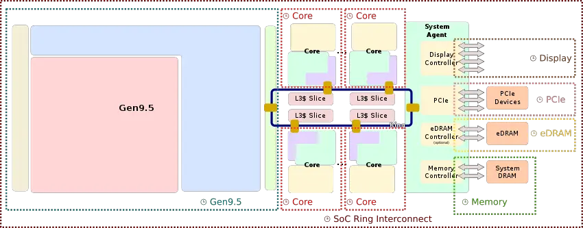
| + | ====== Entire SoC Overview (dual) ====== | ||
| + | [[File:kaby lake soc block diagram (dual).svg|800px]] | ||
| + | |||
| + | ==== Entire SoC Overview (quad) ==== | ||
| + | [[File:kaby lake soc block diagram.svg|900px]] | ||
| + | |||
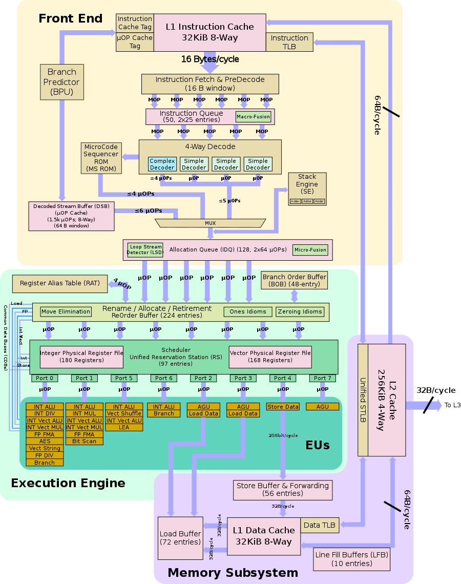
| + | ==== Individual Core ==== | ||
| + | <small>(Core identical to {{\\|Skylake (client)}})</small> | ||
| + | |||
| + | [[File:skylake block diagram.svg|900px]] | ||
| + | |||
| + | ==== Gen9.5 ==== | ||
| + | See {{intel|Gen9.5#Gen9.5|l=arch}}. | ||
=== Memory Hierarchy === | === Memory Hierarchy === | ||
The overall memory structure is identical to {{\\|Skylake}}. | The overall memory structure is identical to {{\\|Skylake}}. | ||
| + | |||
| + | <!-- ===================== START IF YOU CHANGE HERE, CHANGE ON SKYLAKE !! ============================= --> | ||
* Cache | * Cache | ||
| + | ** L0 µOP cache: | ||
| + | *** 1,536 µOPs, 8-way set associative | ||
| + | **** 32 sets, 6-µOP line size | ||
| + | **** statically divided between threads, per core, inclusive with L1I | ||
** L1I Cache: | ** L1I Cache: | ||
| − | *** 32 KiB 8-way set associative | + | *** 32 [[KiB]], 8-way set associative |
| − | **** 64 B line size | + | **** 64 sets, 64 B line size |
| − | |||
**** shared by the two threads, per core | **** shared by the two threads, per core | ||
** L1D Cache: | ** L1D Cache: | ||
| − | *** 32 KiB 8-way set associative | + | *** 32 KiB, 8-way set associative |
| − | *** 64 B line size | + | *** 64 sets, 64 B line size |
*** shared by the two threads, per core | *** shared by the two threads, per core | ||
| − | *** 4 cycles for fastest load-to-use | + | *** 4 cycles for fastest load-to-use (simple pointer accesses) |
| − | *** 64 | + | **** 5 cycles for complex addresses |
| − | *** 32 | + | *** 64 B/cycle load bandwidth |
| + | *** 32 B/cycle store bandwidth | ||
*** Write-back policy | *** Write-back policy | ||
** L2 Cache: | ** L2 Cache: | ||
| − | *** | + | *** Unified, 256 KiB, 4-way set associative |
| + | *** Non-inclusive | ||
| + | *** 1024 sets, 64 B line size | ||
*** 12 cycles for fastest load-to-use | *** 12 cycles for fastest load-to-use | ||
| − | *** | + | *** 64 B/cycle bandwidth to L1$ |
*** Write-back policy | *** Write-back policy | ||
| − | ** L3 Cache: | + | ** L3 Cache/LLC: |
| − | *** Up to 2 MiB Per core, shared across all cores | + | *** Up to 2 MiB Per core, shared across all cores |
*** Up to 16-way set associative | *** Up to 16-way set associative | ||
| + | *** Inclusive | ||
| + | *** 64 B line size | ||
*** Write-back policy | *** Write-back policy | ||
| − | ** | + | *** Per each core: |
| − | *** 64 MiB | + | **** Read: 32 B/cycle (@ ring [[clock]]) |
| + | **** Write: 32 B/cycle (@ ring clock) | ||
| + | *** 42 cycles for fastest load-to-use | ||
| + | ** Side Cache: | ||
| + | *** 64 MiB & 128 MiB [[eDRAM]] | ||
*** Per package | *** Per package | ||
| − | *** Only on the Iris | + | *** Only on the Iris Pro GPUs |
| + | *** Read: 32 B/cycle (@ [[eDRAM]] clock) | ||
| + | *** Write: 32 B/cycle (@ eDRAM clock) | ||
| + | ** System [[DRAM]]: | ||
| + | *** 2 Channels | ||
| + | *** 8 B/cycle/channel (@ memory clock) | ||
| + | *** 42 cycles + 51 ns latency | ||
| − | Kaby Lake TLB consists of dedicated | + | Kaby Lake TLB consists of dedicated L1 TLB for instruction cache (ITLB) and another one for data cache (DTLB). Additionally there is a unified L2 TLB (STLB). |
* TLBs: | * TLBs: | ||
** ITLB | ** ITLB | ||
*** 4 KiB page translations: | *** 4 KiB page translations: | ||
**** 128 entries; 8-way set associative | **** 128 entries; 8-way set associative | ||
| − | **** dynamic | + | **** dynamic partitioning |
*** 2 MiB / 4 MiB page translations: | *** 2 MiB / 4 MiB page translations: | ||
| − | **** 8 entries; fully associative | + | **** 8 entries per thread; fully associative |
**** Duplicated for each thread | **** Duplicated for each thread | ||
** DTLB | ** DTLB | ||
*** 4 KiB page translations: | *** 4 KiB page translations: | ||
**** 64 entries; 4-way set associative | **** 64 entries; 4-way set associative | ||
| − | **** fixed partition | + | **** fixed partition |
*** 2 MiB / 4 MiB page translations: | *** 2 MiB / 4 MiB page translations: | ||
**** 32 entries; 4-way set associative | **** 32 entries; 4-way set associative | ||
| Line 216: | Line 341: | ||
**** 16 entries; 4-way set associative | **** 16 entries; 4-way set associative | ||
**** fixed partition | **** fixed partition | ||
| + | <!-- ===================== END IF YOU CHANGE HERE, CHANGE ON SKYLAKE !! ============================= --> | ||
| + | |||
| + | |||
| + | * '''Note:''' STLB is incorrectly reported as "6-way" by CPUID leaf 2 (EAX=02H). Kaby Lake erratum KBL096 recommends software to simply ignore that value. | ||
| + | |||
| + | == Core == | ||
| + | {{main|intel/microarchitectures/skylake#Core|l1=Skylake § Core}} | ||
| + | Kaby Lake's core is identical to {{\\|Skylake#Core|Skylake's}}. | ||
| + | |||
| + | === Pipeline === | ||
| + | {{main|intel/microarchitectures/skylake#Pipeline|l1=Skylake § Pipeline}} | ||
| + | Kaby Lake's pipeline is identical to {{\\|Skylake#Pipeline|Skylake's}}. | ||
| + | |||
| + | == Configurability == | ||
| + | |||
| + | Kaby Lake builds upon the Skylake architecture, most dies are slight enhancements of their Skylake counterparts. The biggest change is the removal of the high performance quad core GT4 die, which has been replaced by the Kaby Lake G processors. And the introduction of the first low power quad core processor. | ||
| + | |||
| + | <gallery widths=300px heights=150px caption="Physical Layout Breakdown" style="float:right"> | ||
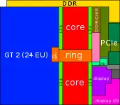
| + | File:2 core lp gt2 skylake.svg|Dual-core die, GT2 GPU, Low Power | ||
| + | File:2 core lp gt3 skylake.svg|Dual-core die, GT3 GPU, Low Power | ||
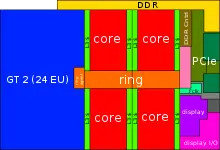
| + | File:4 core lp gt2 kabylake.svg|Quad-core die, GT2 GPU, Low Power | ||
| + | File:dual core hp gt2 skylake.svg|Dual-core die, GT2 GPU, High Power | ||
| + | File:4 core hp gt2 skylake.svg|Quad-core die, GT2 GPU, High Power | ||
| + | </gallery> | ||
| + | |||
| + | {{clear}} | ||
| + | |||
| + | == Graphics == | ||
| + | {{main|intel/microarchitectures/gen9.5|l1=Gen9.5}} | ||
| + | Support for three displays via [[HDMI]] 1.4<ref group=graphics>Note that while there is no native HDMI 2.0 support, Intel did provide somewhat of an awkward solution using an [[LSPCON]] ([[Level Shifter]]/[[Protocol Converter]]) to drive DP to HDMI 1.4 signal + convert HDMI 1.4 to HDMI 2.0. One such solution is the MegaChips MCDP2800.</ref>, [[DisplayPort]] (DP) 1.2, and [[Embedded DisplayPort]] (eDP) 1.4 interfaces. Kaby Lake's biggest enhancement is the addition of native [[fixed function]] HEVC/VP9 decoding for 4K playback at 60fps (10-bit) as well as [[fixed function]] HEVC/VP9 encoding for 4K (8-bit). | ||
| + | |||
| + | {| class="wikitable tc2 tc3" | ||
| + | |- | ||
| + | ! colspan="5" | [[Integrated Graphics Processor]] !! colspan="9" | Standards | ||
| + | |- | ||
| + | ! rowspan="2" | Name !! rowspan="2" | Execution Units !! rowspan="2" | Tier !! rowspan="2" | Series !! rowspan="2" | eDRAM !! colspan="2" | [[Vulkan]] !! colspan="3" | [[Direct3D]] !! colspan="2" | [[OpenGL]] !! colspan="2" | [[OpenCL]] | ||
| + | |- | ||
| + | | Windows || Linux || Windows || Linux || [[High Level Shading Language|HLSL]] || Windows || Linux || Windows || Linux | ||
| + | |- | ||
| + | | {{intel|HD Graphics 610}} || 12 || GT1 || {{intel|Kaby Lake S|S}}, {{intel|Kaby Lake U|U}} || - || rowspan="7" colspan="2" style="text-align: center;" | '''1.0''' || rowspan="7" style="text-align: center;" | '''12''' || rowspan="7" style="text-align: center;" | '''N/A''' || rowspan="7" style="text-align: center;" | '''5.1''' || rowspan="7" style="text-align: center;" | '''4.5''' || rowspan="7" style="text-align: center;" | '''4.5''' || rowspan="7" style="text-align: center;" colspan="1" | '''2.1''' || style="text-align: center;" rowspan="7" | '''2.0''' | ||
| + | |- | ||
| + | | {{intel|HD Graphics 615}} || 24 || GT2|| {{intel|Kaby Lake Y|Y}} || - | ||
| + | |- | ||
| + | | {{intel|HD Graphics 620}} || 24 || GT2 || {{intel|Kaby Lake U|U}}, {{intel|Kaby Lake R|R}} || - | ||
| + | |- | ||
| + | | {{intel|HD Graphics 630}} || 24 || GT2 || {{intel|Kaby Lake S|S}}, {{intel|Kaby Lake H|H}} || - | ||
| + | |- | ||
| + | | {{intel|HD Graphics P630}} || 24 || GT2 || {{intel|Kaby Lake H|H}} || - | ||
| + | |- | ||
| + | | {{intel|Iris Plus Graphics 640}} || 48 || GT3e|| {{intel|Kaby Lake U|U}} || 64 MiB | ||
| + | |- | ||
| + | | {{intel|Iris Plus Graphics 650}} || 48 || GT3e || {{intel|Kaby Lake U|U}} || 64 MiB | ||
| + | |} | ||
| + | |||
| + | <references group=graphics /> | ||
| + | ==== Hardware Accelerated Video ==== | ||
| + | {{kaby lake hardware accelerated video table}} | ||
| + | |||
| + | == Sockets/Platform == | ||
| + | {{intel|Kaby Lake Y|l=core}} and {{intel|Kaby Lake U|U|l=core}} are single-chip solutions. {{intel|Kaby Lake Y|Y|l=core}} chips utilize a 2-die [[multi-chip package]] (MCP) whereas the {{intel|Kaby Lake U|l=core}}'s are either 2 or 3-die MCP configuration. The 3 die chip configuration are for the Iris [[IGP]]s which incorporate an on-package cache (OPC) in addition to the hub. Communication from the CPU to the hub on those chips are done via a lightweight On-Package Interconnect (OPI) interface. {{intel|Kaby Lake S|l=core}} and {{intel|Kaby Lake H|H|l=core}} are a two-chip solution linked together via Intel's standard [[DMI 3.0]] bus interface which utilizes 4 of the CPU's 20 [[PCIe]] 3.0 lanes (having a transfer rate of 8 GT/s per lane). Only {{intel|Kaby Lake S|l=core}} (used on mainstream desktop processors) are not soldered onto the [[motherboard]] and can be interchanged/replaced. | ||
| + | {| class="wikitable" style="text-align: center;" | ||
| + | |- | ||
| + | ! !! Core !! Socket !! Permanent !! Platform !! Chipset !! Bus | ||
| + | |- | ||
| + | | [[File:kaby lake y (back).png|100px|link=intel/cores/kaby_lake_y]] || {{intel|Kaby Lake Y|l=core}} || {{intel|BGA-1515}} || Yes || 1-chip || rowspan="3" | N/A || rowspan="3" | OPI | ||
| + | |- | ||
| + | | [[File:kaby lake u (back; standard).png|100px|link=intel/cores/kaby_lake_u]] || {{intel|Kaby Lake U|l=core}} || rowspan="2" | {{intel|BGA-1356}} || rowspan="2" | Yes || rowspan="2" | 1-chip | ||
| + | |- | ||
| + | | [[File:kaby lake r (back).png|100px|link=intel/cores/kaby_lake_r]] || {{intel|Kaby Lake R|l=core}} | ||
| + | |- | ||
| + | | [[File:kaby lake h (back).png|100px|link=intel/cores/kaby_lake_h]] || {{intel|Kaby Lake H|l=core}} || {{intel|BGA-1440}} || Yes || 2-chip || rowspan="2" | {{intel|Sunrise Point}}<ref group="c">Requires a firmware update in order to work with Kaby Lake chips</ref><br>{{intel|Union Point}} || rowspan="4" | [[DMI 3.0]] | ||
| + | |- | ||
| + | | rowspan="2" | [[File:kaby lake s (back).png|100px|link=intel/cores/kaby_lake_s]] || {{intel|Kaby Lake S|l=core}} || {{intel|LGA-1151}} || No || 2-chip | ||
| + | |- | ||
| + | | {{intel|Kaby Lake DT|l=core}} || {{intel|LGA-1151}} || No || 2-chip || Xeon {{intel|Sunrise Point}}<br>Xeon {{intel|Union Point}} | ||
| + | |- | ||
| + | | [[File:skylake x (back).png|100px|link=intel/cores/kaby_lake_x]] || {{intel|Kaby Lake X|l=core}} || {{intel|LGA-2066}} || No || 2-chip || {{intel|Lewisburg}} | ||
| + | |} | ||
| + | |||
| + | <references group="c" /> | ||
| + | |||
| + | |||
| + | === Packages === | ||
| + | {| class="wikitable" | ||
| + | |- | ||
| + | ! Core !! Die Type !! Package !! Dimensions | ||
| + | |- | ||
| + | | {{intel|Kaby Lake H|l=core}} || 4+2 || rowspan="2" | {{intel|FCBGA-1440}} || rowspan="2" | 42 mm x 28 mm x 1.46 mm | ||
| + | |- | ||
| + | | {{intel|Kaby Lake H|l=core}} || 2+2 | ||
| + | |- | ||
| + | | {{intel|Kaby Lake S|l=core}} || 4+2 || rowspan="2" | {{intel|FCLGA-1151}} || rowspan="2" | 37.5 mm x 37.5 mm x 4.4 mm | ||
| + | |- | ||
| + | | {{intel|Kaby Lake S|l=core}} || 2+2 | ||
| + | |} | ||
| + | |||
| + | == Clock domains == | ||
| + | Kaby Lake is divided into a number of [[clock domains]], each controlling the clock frequency of their respective unit in the processor. All clock domains are some multiple of the [virtual] bus clock ([[BCLK]]). | ||
| + | |||
| + | * '''BCLK''' - Bus/Base Clock - The system bus interface frequency (once upon a time referred to the actual [[FSB]] speed, it now serves as only a base clock reference for all other clock domains). The base clock is 100 MHz. | ||
| + | * '''Core Clock''' - The frequency at which the core and the [[L1]]/[[L2]] caches operate at. (Frequency depends on the model and is represented as a multiple of BCLK). | ||
| + | * '''Ring Clock''' - The frequency at which the ring interconnect and [[L3$|LLC]] operate at. Data from/to the individual cores are read/written into the L3 at a rate of 32B/cycle operating at Ring Clock frequency. | ||
| + | * '''IGP Clock''' - The frequency at which the [[integrated graphics]] ({{\\|Gen9}} GPU) operates at. Data from/to the GPU are read/written into the LLC at a rate of 64B/cycle operating at this frequency as well. | ||
| + | * '''eDRAM Clock''' - The frequency at which the [[embedded DRAM]] operates at (only available for certain models). Data is read/written from/to the LLC at a rate of 32B/cycle operating at this frequency as well. | ||
| + | * '''MemClk''' - Memory Clock - The frequency at which the system DRAM operates at. DRAM data is transfered at a rate of 8B/cycle operating at MemClk frequency. | ||
| + | |||
| + | [[File:kaby lake soc clock domain block diagram.svg|850px]] | ||
| + | |||
| + | === Overclocking === | ||
| + | See {{intel|Skylake#Overclocking|Skylake §Overclocking|l=arch}}. | ||
| + | |||
| + | == Kaby Lake G == | ||
| + | [[File:kaby lake g with amd radeon package.png|right|300px]] | ||
| + | {{main|intel/cores/kaby lake g|l1=Kaby Lake G Core}} | ||
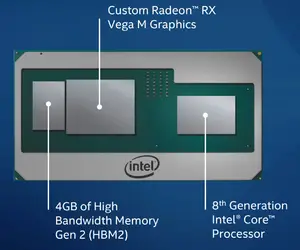
| + | At CES 2018 (January 7) Intel announced ''8th Gen Intel Core with Radeon RX Vega M'', formerly code name {{intel|Kaby Lake G|l=core}}. Those parts combine Intel's {{intel|Kaby Lake H|l=core}} parts with and [[AMD]] {{amd|Vega|l=arch}} GPU as well as [[high-bandwidth memory]] 2. | ||
| + | |||
| + | All parts incorporate 4 GiB of [[HBM 2]] along with an [[AMD]] {{amd|Vega|l=arch}} GPU. The HBM2 and GPU are interconnected using Intel's [[EMIB]], however, the CPU and GPU are connected using standard in-package wires over standard PCIe 3.0. x8 lanes are permanently reserved for direct GPU-CPU communication. This leaves x8 additional lanes for all other peripherals that need direct connection to the CPU. | ||
| + | |||
| + | [[File:intel-radeon emib solution.svg|650px]] | ||
| + | |||
| + | Intel claims that the use of HBM2 instead of [[GDDR5]] results in 80% less power. It's worth noting that since those are {{intel|Kaby Lake H|l=core}} parts with {{amd|Radeon}} Graphics, they effectively have two GPUs and both GPUs are usable. Fairly significant power saving can be achieved by defaulting to the integrated graphics when high performance is not required. In total there are 3 display outputs from the integrated graphics and an additional 6 outputs from the Radeon graphics for a total of 9. | ||
| + | |||
| + | By moving from [[GDDR5]] to [[HBM 2]] and going to higher integration by packing everything into a single package, Intel has achieved considerably higher density. Intel reported that around 1900 mm² (~3 in²) board space saving has been achieved which is rather significant for ultra-light and ultra-thin notebooks and tablets where logic board area reduction is important. Additionally, this reduces the [[bills of material|BOM]] for OEMs. | ||
| + | |||
| + | [[File:kaby lake g board space saving.png|700px]] | ||
| + | |||
| + | === Dynamic Tuning === | ||
| + | [[File:intel dynamic tuning.png|right|250px]] | ||
| + | {{main|intel/dynamic tuning|l1=Dynamic Tuning}} | ||
| + | With Kaby Lake G Intel introduced Dynamic Tuning which is a way of managing the entire package power consumption by adjusting the power policies of the GPU and CPU depending on the application. Applications that make no use of the discrete GPU will see the majority of the package power budget allocated for the CPU to accelerate that workloads while things like gaming will shift the power in favor of GPU acceleration. The feature is implemented entirely in software. | ||
| + | |||
| + | === Graphics === | ||
| + | {{intel|Kaby Lake G|l=core}} has one of two possible AMD {{amd|Radeon}} graphics based on the {{amd|Vega|l=arch}} microarchitecture. | ||
| + | |||
| + | {| class="wikitable" | ||
| + | ! colspan="3" | Radeon RX Vega | ||
| + | |- | ||
| + | ! Graphics !! Radeon RX Vega M GH !! Radeon RX Vega M GL | ||
| + | |- | ||
| + | | Architecture || {{amd|Vega|Vega M|l=arch}} || {{amd|Vega|Vega M|l=arch}} | ||
| + | |- | ||
| + | | Compute Units || 24 || 20 | ||
| + | |- | ||
| + | | Stream Processors || 1,536 || 1,280 | ||
| + | |- | ||
| + | | ROPs || 64 pixels/clock || 32 pixels/clock | ||
| + | |- | ||
| + | | Base Clock || 1,063 MHz || 931 MHz | ||
| + | |- | ||
| + | | Boost Frequency || 1,190 MHz || 1,011 MHz | ||
| + | |- | ||
| + | | Peak Performance || 3.7 TFLOPS || 2.6 TFLOPS | ||
| + | |- | ||
| + | ! colspan="3" | HBM 2 | ||
| + | |- | ||
| + | | Capacity || 4 GiB || 4 GiB | ||
| + | |- | ||
| + | | Clock || 800 MHz || 700 MHz | ||
| + | |- | ||
| + | | Bandwidth || 204.8 GB/s || 179.2 GB/s | ||
| + | |} | ||
== Die == | == Die == | ||
| − | Dual Core Kaby Lake | + | Kaby Lake desktop and mobile come and [[2 cores|2]] and [[4 cores|4]] cores. Each variant has its own die. One of the most noticeable changes on die is the amount of die space allocated to the [[GPU]]. The major components of the die are: |
| + | |||
| + | * System Agent | ||
| + | * CPU Core | ||
| + | * Ring bus interconnect | ||
| + | * Memory Controller | ||
| + | |||
| + | === System Agent === | ||
| + | The System Agent (SA) contains the Image Processing Unit (IPU), the Display Engine (DE), and the I/O bus. Note that the mainstream desktop (i.e., [[quad-core]] die) does not have an IPU (The memory controller actually occupies a portion of where it would otherwise be). | ||
| + | |||
| + | <div> | ||
| + | <div style="text-align: center; display: inline-block;"> | ||
| + | '''Dual-Core Die''' | ||
| + | <div style="float: left; margin: 10px;">[[File:kaby lake 2c sa.png|150px]]</div> | ||
| + | <div style="float: left; margin: 10px;">[[File:kaby lake 2c sa (annotated).png|150px]]</div> | ||
| + | </div> | ||
| + | <div style="text-align: center; display: inline-block;"> | ||
| + | '''Quad-Core Die''' | ||
| + | <div style="float: left; margin: 10px;">[[File:kaby lake 4c sa.png|150px]]</div> | ||
| + | <div style="float: left; margin: 10px;">[[File:kaby lake 4c sa (annotated).png|150px]]</div> | ||
| + | </div> | ||
| + | <div style="text-align: center; display: inline-block;"> | ||
| + | '''Quad-Core ({{intel|Kaby Lake R|l=core}}) Die''' | ||
| + | <div style="float: left; margin: 10px;">[[File:kaby lake r sa.png|150px]]</div> | ||
| + | <div style="float: left; margin: 10px;">[[File:kaby lake r sa (annotated).png|150px]]</div> | ||
| + | </div> | ||
| + | </div> | ||
| + | {{clear}} | ||
| + | |||
| + | === Integrated Graphics === | ||
| + | The [[integrated graphics]] takes up the largest portion of the die. The normal [[dual-core]] and [[quad-core]] dies come with 24 EU {{\\|Gen9.5}} GPU (with 12 units disabled on the low end models). | ||
| + | |||
| + | <div style="text-align: center; display: inline-block;"> | ||
| + | <div style="float: left; margin: 10px;">[[File:kaby lake gpu.png|400px]]</div> | ||
| + | <div style="float: left; margin: 10px;">[[File:kaby lake gpu (annotated).png|450px]]</div> | ||
| + | </div> | ||
| + | |||
| + | ==== Layout Difference from Skylake ==== | ||
| + | The majority of the enhancements to Kaby Lake comes from the Unslice portion of the {{\\|Gen9.5}} integrated GPU. The shaded region marked in green indicates new/modified physical layout changes. The rest of the die, shaded in red, is unchanged from {{\\|Skylake}}. | ||
| − | + | [[File:kaby lake skylake gpu diff.png|450px]] | |
| + | === Dual-Core === | ||
| + | Die shot of the [[dual-core]] {{\\|Gen9.5|GT2}} Kaby Lake processors. Those are found in mobile models, and entry-level/budget processors: | ||
| − | + | * [[14 nm process|14 nm+ process]] | |
| + | * 11 metal layers | ||
| + | * 2 CPU cores + 24 GPU EUs | ||
| + | : [[File:kaby lake (dual core).png|650px]] | ||
| + | |||
| + | |||
| + | : [[File:kaby lake (dual core) (annotated).png|650px]] | ||
| + | |||
| + | === Quad-Core === | ||
| + | Die shot of the [[quad-core]] {{\\|Gen9.5|GT2}} Kaby Lake processors. Those are found in almost all mainstream desktop processors. | ||
| + | |||
| + | * [[14 nm process|14 nm+ process]] | ||
| + | * 11 metal layers | ||
| + | * ~9,21 mm x ~13,50 mm | ||
| + | * ~126 mm² die size | ||
| + | * 4 CPU cores + 24 GPU EUs | ||
| + | |||
| + | : [[File:kaby lake (quad core).png|class=wikichip_ogimage|650px]] | ||
| + | |||
| + | |||
| + | : [[File:kaby lake (quad core) (annotated).png|650px]] | ||
| + | |||
| + | === Quad-Core (Mobile {{intel|Kaby Lake R|l=core}}) === | ||
| + | With the introduction of {{intel|Kaby Lake R|l=core}}, a new quad-core die was introduced. It's worth pointing out that this die is very different from the standard desktop quad-core die. Other than likely being optimized specifically for this market segment, this die also incorporates {{\\|Skylake (client)#Image Processing Unit (IPU)|the IPU}} in the System Agent. Previously this integration was only found in the dual-core dies which were used for {{intel|Skylake U|l=core}} and {{intel|Kaby Lake U|l=core}}. | ||
| + | |||
| + | * [[14 nm process|14 nm+ process]] | ||
| + | * 11 metal layers | ||
| + | * 123 mm² die size | ||
| + | * 4 CPU cores + 24 GPU EUs | ||
| + | |||
| + | : [[File:kaby lake r die shot.png|650px]] | ||
| + | |||
| + | |||
| + | : [[File:kaby lake r die shot (annotated).png|650px]] | ||
| + | |||
| + | === Additional Shots === | ||
| + | Additional die and wafer shots provided by Intel: | ||
| + | |||
| + | <gallery mode=slideshow> | ||
| + | File:kaby lake silicon wafer.jpg|Kaby Lake silicon [[wafer]] with 7th generation core processor dies. | ||
| + | File:intel kaby lake r wafer.png|Wafer shot of {{intel|Kaby Lake R|l=core}}, 8th generation core. | ||
| + | </gallery> | ||
== All Kaby Lake Chips == | == All Kaby Lake Chips == | ||
| Line 235: | Line 602: | ||
--> | --> | ||
{{comp table start}} | {{comp table start}} | ||
| − | <table class="comptable sortable | + | <table class="comptable sortable tc18 tc19 tc20 tc21 tc22 tc23"> |
| − | <tr class="comptable-header"><th> </th><th colspan=" | + | <tr class="comptable-header"><th> </th><th colspan="25">Kaby Lake Chips</th></tr> |
| − | <tr class="comptable-header"><th> </th><th colspan=" | + | <tr class="comptable-header"><th> </th><th colspan="13">Main processor</th><th colspan="3">IGP</th><th colspan="9">Major Feature Diff</th></tr> |
| − | <tr class="comptable-header"><th class="unsortable">Model</th><th>Launched</th><th>Price</th><th>Family</th><th>Platform</th><th>Core</th><th> | + | <tr class="comptable-header"><th class="unsortable">Model</th><th>Launched</th><th data-sort-type="currency">Price</th><th>Family</th><th>Platform</th><th>Core</th><th data-sort-type="number">Cores</th><th data-sort-type="number">Threads</th><th data-sort-type="number">L3$</th><th data-sort-type="number">L4$</th><th data-sort-type="number">TDP</th><th data-sort-type="number">Freq</th><th data-sort-type="number">Turbo</th><th data-sort-type="number">Max Mem</th><th>Name</th><th data-sort-type="number">Freq</th><th data-sort-type="number">Turbo</th><th>[[ECC]]</th><th>{{intel|turbo boost|TBT}}</th><th>HT</th><th>AVX</th><th>AVX2</th><th>TXT</th><th>TSX</th><th>vPro</th><th>VT-d</th></tr> |
| − | <tr class="comptable-header comptable-header-sep"><th> </th><th colspan=" | + | <tr class="comptable-header comptable-header-sep"><th> </th><th colspan="25">[[Uniprocessors]]</th></tr> |
| − | {{#ask: [[Category:microprocessor models by intel]] [[instance of::microprocessor]] [[microarchitecture::Kaby Lake]] [[max cpu count::1]] | + | {{#ask: [[Category:microprocessor models by intel]] [[instance of::microprocessor]] [[microarchitecture::Kaby Lake]] [[max cpu count::1]] [[core name::!Kaby Lake R]][[core name::!Kaby Lake G]] |
| + | |?full page name | ||
| + | |?model number | ||
| + | |?first launched | ||
| + | |?release price | ||
| + | |?microprocessor family | ||
| + | |?platform | ||
| + | |?core name | ||
| + | |?core count | ||
| + | |?thread count | ||
| + | |?l3$ size | ||
| + | |?l4$ size | ||
| + | |?tdp | ||
| + | |?base frequency#GHz | ||
| + | |?turbo frequency (1 core)#GHz | ||
| + | |?max memory#GiB | ||
| + | |?integrated gpu | ||
| + | |?integrated gpu base frequency | ||
| + | |?integrated gpu max frequency | ||
| + | |?has_ecc_memory_support | ||
| + | |?has intel turbo boost technology 2_0 | ||
| + | |?has simultaneous multithreading | ||
| + | |?has advanced vector extensions | ||
| + | |?has advanced vector extensions 2 | ||
| + | |?has intel trusted execution technology | ||
| + | |?has transactional synchronization extensions | ||
| + | |?has intel vpro technology | ||
| + | |?has_intel_vt-d_technology | ||
| + | |format=template | ||
| + | |template=proc table 3 | ||
| + | |searchlabel= | ||
| + | |sort=microprocessor family, model number | ||
| + | |order=asc,asc | ||
| + | |userparam=27:19 | ||
| + | |mainlabel=- | ||
| + | |limit=100 | ||
| + | }} | ||
| + | <tr class="comptable-header comptable-header-sep"><th> </th><th colspan="25">8th Generation ({{intel|Kaby Lake R|Kaby Lake Refresh|l=core}})</th></tr> | ||
| + | {{#ask: [[Category:microprocessor models by intel]] [[instance of::microprocessor]] [[microarchitecture::Kaby Lake]] [[max cpu count::1]] [[core name::Kaby Lake R]] | ||
| + | |?full page name | ||
| + | |?model number | ||
| + | |?first launched | ||
| + | |?release price | ||
| + | |?microprocessor family | ||
| + | |?platform | ||
| + | |?core name | ||
| + | |?core count | ||
| + | |?thread count | ||
| + | |?l3$ size | ||
| + | |?l4$ size | ||
| + | |?tdp | ||
| + | |?base frequency#GHz | ||
| + | |?turbo frequency (1 core)#GHz | ||
| + | |?max memory#GiB | ||
| + | |?integrated gpu | ||
| + | |?integrated gpu base frequency | ||
| + | |?integrated gpu max frequency | ||
| + | |?has_ecc_memory_support | ||
| + | |?has intel turbo boost technology 2_0 | ||
| + | |?has simultaneous multithreading | ||
| + | |?has advanced vector extensions | ||
| + | |?has advanced vector extensions 2 | ||
| + | |?has intel trusted execution technology | ||
| + | |?has transactional synchronization extensions | ||
| + | |?has intel vpro technology | ||
| + | |?has_intel_vt-d_technology | ||
| + | |format=template | ||
| + | |template=proc table 3 | ||
| + | |searchlabel= | ||
| + | |sort=microprocessor family, model number | ||
| + | |order=asc,asc | ||
| + | |userparam=27:19 | ||
| + | |mainlabel=- | ||
| + | |limit=100 | ||
| + | }} | ||
| + | <tr class="comptable-header comptable-header-sep"><th> </th><th colspan="25">8th Generation ({{intel|Kaby Lake G|Kaby Lake Graphics|l=core}})</th></tr> | ||
| + | {{#ask: [[Category:microprocessor models by intel]] [[instance of::microprocessor]] [[microarchitecture::Kaby Lake]] [[max cpu count::1]] [[core name::Kaby Lake G]] | ||
|?full page name | |?full page name | ||
|?model number | |?model number | ||
| Line 250: | Line 693: | ||
|?core count | |?core count | ||
|?thread count | |?thread count | ||
| − | |? | + | |?l3$ size |
| + | |?l4$ size | ||
|?tdp | |?tdp | ||
|?base frequency#GHz | |?base frequency#GHz | ||
| Line 258: | Line 702: | ||
|?integrated gpu base frequency | |?integrated gpu base frequency | ||
|?integrated gpu max frequency | |?integrated gpu max frequency | ||
| − | |?has intel turbo boost technology | + | |?has_ecc_memory_support |
| + | |?has intel turbo boost technology 2_0 | ||
|?has simultaneous multithreading | |?has simultaneous multithreading | ||
| + | |?has advanced vector extensions | ||
| + | |?has advanced vector extensions 2 | ||
| + | |?has intel trusted execution technology | ||
| + | |?has transactional synchronization extensions | ||
| + | |?has intel vpro technology | ||
| + | |?has_intel_vt-d_technology | ||
|format=template | |format=template | ||
|template=proc table 3 | |template=proc table 3 | ||
|searchlabel= | |searchlabel= | ||
| − | |userparam=19 | + | |sort=microprocessor family, model number |
| + | |order=asc,asc | ||
| + | |userparam=27:19 | ||
|mainlabel=- | |mainlabel=- | ||
|limit=100 | |limit=100 | ||
| Line 272: | Line 725: | ||
== Documents == | == Documents == | ||
| − | * [[:File:7th Generation Intel® Core™ Processor Product Brief.pdf|7th Generation | + | === 7th Generation === |
| − | * [[:File:7th Generation Intel® Core™ Processor Y-Series and U-Series Product Brief.pdf|7th Generation | + | * [[:File:7th-gen-intel-core-january-product-brief.pdf|7th gen intel core & Intel Xeon processor briefing]] |
| − | * [[:File:7th Gen Intel® Core™ Processor Family Fact Sheet.pdf|7th Gen | + | * [[:File:7th Generation Intel® Core™ Processor Product Brief.pdf|7th Generation Intel Core Processor Product Brief]] |
| + | * [[:File:7th-gen-intel-core-january-fact-sheet.pdf|7th Gen Intel Core & Xeon Processor Family Fact Sheet]] | ||
| + | * [[:File:7th-gen-intel-core-vpro-product-brief.pdf|7th Generation Intel Core vPro Processor Briefing]] | ||
| + | * [[:File:7th Generation Intel® Core™ Processor Y-Series and U-Series Product Brief.pdf|7th Generation Intel Core Processor Y-Series and U-Series Product Brief]] | ||
| + | * [[:File:7th Gen Intel® Core™ Processor Family Fact Sheet.pdf|7th Gen Intel Core Processor Family Fact Sheet]] | ||
| + | * [[:File:7th-generation-core-processor-deskop-iot-platform-brief.pdf|7th Generation Intel Core Processor-Based Platforms for Internet of Things (IoT) Solutions Platform brief]] | ||
| + | * [[:File:how-to-watch-4k-uhd-premium-content-with-your-pc.pdf|HOW TO WATCH 4K ULTRA HD (UHD) PREMIUM CONTENT WITH YOUR PC]] | ||
| + | === 8th Generation === | ||
| + | * [[:File:kaby-lake-r-product-brief.pdf|Kaby Lake R Product Brief]] | ||
| + | * [[:File:8th-gen-intel-core-product-overview.pdf|8th generation Core family product overview]] | ||
| + | * [[:File:8th-gen-radeon-rx-vega-m-product-overview.pdf|8th Gen Intel® Core processors With RadeonTM RX Vega M Graphics]] | ||
| + | |||
| + | == Bibliography == | ||
| + | * Intel Developer Forum 2015, San Francisco, August 18-20, 2015 | ||
| + | * Intel Technology and Manufacturing Day, March 28, 2017 | ||
| + | * 8th Generation core announcement, August 21, 2017 | ||
| + | * IEEE Hot Chips 30 Symposium (HCS) 2018. | ||
| + | * Schor, David. (September, 2018). "''[https://fuse.wikichip.org/news/1634/hot-chips-30-intel-kaby-lake-g/ Hot Chips 30: Intel Kaby Lake G]''" | ||
| + | |||
| + | == Artwork == | ||
| + | <gallery> | ||
| + | File:7th Gen Intel Core i3 unlocked box.png|Kaby Lake offers the first unlocked {{intel|Core i3}} model. | ||
| + | File:7th Gen Intel Core i7 unlocked box - front.png | ||
| + | File:7th Gen Intel Core i7 unlocked box - back.png | ||
| + | File:7th Gen Intel Core family.jpg | ||
| + | File:7th Gen-Navoy-1.JPG|Navin Shenoy, Intel corporate vice president and general manager for its Client Computing Group | ||
| + | File:7th Gen-Navoy-2.JPG | ||
| + | File:7th Gen-Navoy-3.JPG | ||
| + | File:7th Gen-Walker-1.JPG|Chris Walker, Intel vice president for its Client Computing Group and general manager of notebook product marketing | ||
| + | File:7th Gen-Walker-2.JPG | ||
| + | File:7th Gen-Walker-3.JPG | ||
| + | File:7th Gen-water-1.JPG | ||
| + | File:7th-gen-wafer.jpg|7th gen core silicon wafers | ||
| + | </gallery> | ||
== See also == | == See also == | ||
* {{amd|microarchitectures/zen|AMD's Zen}} | * {{amd|microarchitectures/zen|AMD's Zen}} | ||
Latest revision as of 09:41, 8 April 2024
| Edit Values | |
| Kaby Lake µarch | |
| General Info | |
| Arch Type | CPU |
| Designer | Intel |
| Manufacturer | Intel |
| Introduction | August 30, 2016 |
| Process | 14 nm |
| Core Configs | 2, 4 |
| Pipeline | |
| Type | Superscalar |
| Speculative | Yes |
| Reg Renaming | Yes |
| Stages | 14-19 |
| Instructions | |
| ISA | x86-64 |
| Extensions | MOVBE, MMX, SSE, SSE2, SSE3, SSSE3, SSE4.1, SSE4.2, POPCNT, AVX, AVX2, AES, PCLMUL, FSGSBASE, RDRND, FMA3, F16C, BMI, BMI2, VT-x, VT-d, TXT, TSX, RDSEED, ADCX, PREFETCHW, CLFLUSHOPT, XSAVE, SGX, MPX |
| Cache | |
| L1I Cache | 32 KiB/core 8-way set associative |
| L1D Cache | 32 KiB/core 8-way set associative |
| L2 Cache | 256 KiB/core 4-way set associative |
| L3 Cache | 2 MiB/core Up to 16-way set associative |
| Side Cache | 64 MiB/package on Iris Plus GPUs only |
| Cores | |
| Core Names | Kaby Lake Y, Kaby Lake U, Kaby Lake R, Kaby Lake H, Kaby Lake G, Kaby Lake S, Kaby Lake DT, Kaby Lake X |
| Succession | |
Kaby Lake (KBL) is Intel's successor to Skylake, an enhanced 14 nm process microarchitecture for mainstream desktops and mobile devices. Kaby Lake is the first "Optimization" released as part of Intel's PAO model. The microarchitecture was developed by Intel's R&D center in Haifa, Israel. Cannon Lake was originally set to replace Skylake as the next microarchitecture using a 10 nm process, however Intel later revised their roadmap to include Kaby Lake (with Cannon Lake being pushed back to 2018).
For desktop and mobile, Kaby Lake is branded as 7th Generation Intel Core i3, Core i5. and Core i7 processors. For workstation class processors, Intel branded it as Xeon E3 v6. There are no Kaby Lake-based server microprocessors.
Contents
Codenames[edit]
| Core | Abbrev | Platform | Description | Graphics | Target |
|---|---|---|---|---|---|
| Kaby Lake Y | KBL-Y | Extremely low power | GT2 | 2-in-1s detachable, tablets, and computer sticks | |
| Kaby Lake U | KBL-U | Ultra-low Power | GT2/GT3 | Light notebooks, portable All-in-Ones (AiOs), Minis, and conference room | |
| Kaby Lake R | KBL-R | Ultra-low Power | GT2 | Kaby Lake U Refresh | |
| Kaby Lake H | KBL-H | High-performance Graphics | GT2/GT3 | Ultimate mobile performance, mobile workstations | |
| Kaby Lake S | KBL-S | Performance-optimized lifestyle | GT2/GT3 | Desktop performance to value, AiOs, and minis | |
| Kaby Lake G | KBL-G | Pedlow | Gaming Chip | GT2 + AMD Vega | Kaby Lake + Radeon Vega 20/24 |
| Kaby Lake X | KBL-X | Basin Falls | Extreme Performance | High-end desktops & enthusiasts market | |
| Kaby Lake DT | KBL-DT | Greenlow | Workstation | GT2 | Workstations & entry-level servers |
Brands[edit]
Intel released Kaby Lake under 6 main brand families:
| Logo | Family | General Description | Differentiating Features | |||||
|---|---|---|---|---|---|---|---|---|
| Cores | HT | AVX | AVX2 | TBT | ECC | |||
 |
Celeron | Entry-level Budget | dual | ✘ | ✘ | ✘ | ✘ | ✘ |
 |
Pentium | Budget (Mobile) | dual | ✔ | ✘ | ✘ | ✘ | ✘ |
| Budget (Desktop) | ✔ | ✘ | ✘ | ✘ | ✔ | |||
 |
Pentium Gold | Budget (Mobile) | dual | ✔ | ✘ | ✘ | ✘ | ✘ |
| Budget (Desktop) | ✔ | ✘ | ✘ | ✘ | ✔ | |||
 |
Core i3 | Low-end Performance | dual | ✔ | ✔ | ✔ | ✘ | ✘ |
| Low-end Performance (E Series) | ✔ | ✔ | ✔ | ✘ | ✔ | |||
 |
Core i5 | Mid-range Performance | dual | ✔ | ✔ | ✔ | ✔ | ✘ |
| quad | ✘ | ✔ | ✔ | ✔ | ✘ | |||
| Mid-range Performance (KBL-R) | ✔ | ✔ | ✔ | ✔ | ✘ | |||
 |
Core i7 | High-end Performance | dual | ✔ | ✔ | ✔ | ✔ | ✘ |
| quad | ✔ | ✔ | ✔ | ✔ | ✘ | |||
 |
Xeon E3 | Workstation high-performance/dense servers | quad | ✔ | ✔ | ✔ | ✔ | ✔ |
Release Dates[edit]
Kaby Lake is set to be released in two phases. The first phase was announced in August of 2016 and was primarily aimed at various low-power consumer products such as light notebooks and 2-in-1s. Those devices are powered by Kaby Lake Y and Kaby Lake U CPUs. Intel released mainstream Kaby Lake S and Kaby Lake H processors on January 3, 2017 in time for CES 2017. The enthusiast version, Kaby Lake X, was introduced during Computex Taipei 2017.
On August 21 2017, Intel introduced 8th generation mobile processors (Kaby Lake Refresh) which is also based on the same microarchitecture and doubled the cores (4 from 2) of many mainstream mobile microprocessors.
Process Technology[edit]
| 14 nm Manufacturing Fabs | |
|---|---|
| Fab | Location |
| D1X | Hillsboro, Oregon |
| D1D | Hillsboro, Oregon |
| D1C | Hillsboro, Oregon |
| Fab 32 | Chandler, Arizona |
| Fab 24 | Leixlip, Ireland |
- See also: Broadwell § Process Technology and 14 nm lithography process
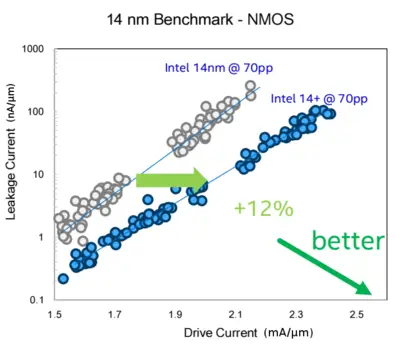
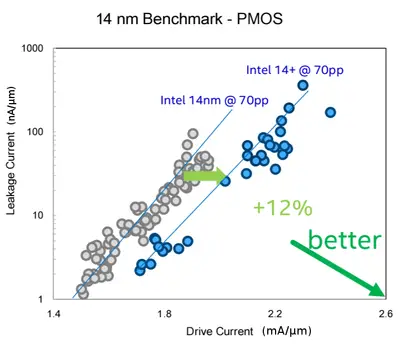
Kaby Lake uses a modified and improved 14 nm process used for the Broadwell microarchitecture (And Skylake). Intel calls the modified process "14nm+". The new process has improved transistor channel strain. The various enhancements improve performance without increasing the capacitance (i.e., active power characteristics). These changes allowed Intel to increase the maximum frequencies of all models by around 100 to 300 megahertz which gives many single-thread applications a modest performance increase. Overall transistors improvement allowed for +12% drive current.
Compatibility[edit]
There are no official drivers by Intel for Windows 7 or Windows 8. Microsoft announced that only Windows 10 will have support for Kaby Lake. Linux added initial support for Kaby Lake starting with Linux Kernel 4.5.
| Vendor | OS | Version | Notes |
|---|---|---|---|
| Microsoft | Windows | Windows 7 | No Support |
| Windows 8 | No Support | ||
| Windows 10 | Support | ||
| Linux | Linux | Kernel 4.5 | Initial Support (Fedora 24, Yocto v2.2, ..) |
| Chromium | Chromium | Support | |
| Wind River | VxWorks | VxWorks 7 | Support |
Compiler support[edit]
| Compiler | Arch-Specific | Arch-Favorable |
|---|---|---|
| ICC | -march=skylake |
-mtune=skylake
|
| GCC | -march=skylake |
-mtune=skylake
|
| LLVM | -march=skylake |
-mtune=skylake
|
| Visual Studio | /arch:AVX2 |
/tune:skylake
|
CPUID[edit]
| Core | Extended Family |
Family | Extended Model |
Model | Stepping |
|---|---|---|---|---|---|
| Y/U/R | 0 | 0x6 | 0x8 | 0xE | 0x9 |
| Family 6 Model 142 Stepping 9 | |||||
| DT/H/S/X | 0 | 0x6 | 0x9 | 0xE | 0x9 |
| Family 6 Model 158 Stepping 9 | |||||
Architecture[edit]
- See also: Skylake § Key changes from Broadwell
While there is no change in pure IPC over Skylake and the actual microarchitecture is largely the same, Intel introduced a number of enhancements in Kaby Lake. Note that because of the improvements done to the process and the uplift in binning, it is the mostly the ultra-low power (i.e. mobile) processors that will see the most substantial gain. Likewise, the high-end models will see very little gain. The enhanced manufacturing process allowed Kaby Lake chips to be highly overclockable with models such as the Core i7-7700K capable of comfortably reaching 5 GHz for many people with a reasonable cooling setup.
Key changes from Skylake[edit]
- Enhanced "14nm+" process results in ~15% higher frequency (100 to 300 MHz increase across the board, same price)
- Same IPC as Skylake (i.e. performance/MHz is unchanged)
- 10x performance/Watt over Nehalem (Up from 8x)
- SkyLake's Speed Shift implementation is significantly improved, cutting responsiveness by as much as 66% (down to just ~10-15ms to peak frequency).
- Mainstream chipset (See § Sockets)
- Sunrise Point (100 series) → Union Point (200 Series)
- Sunrise Point is still compatible (may need firmware update)
- Added support for Optane Technology
- Sunrise Point (100 series) → Union Point (200 Series)
- Memory
- Faster memory for mainstream desktops (i.e., Kaby Lake S) DDR4-2400 (from DDR4-2133)
- Faster memory for high-perf mobile (i.e., Kaby Lake H) DDR4-2400 (from DDR4-2133)
- Interfaces
- Embedded DisplayPort (eDP) now supports eDP Standard 1.4 (From 1.3 in Skylake)
- Gen 9.5 GPUs
- Iris Plus now support HDMI (1.4a) 4096x2304 @ 30 Hz (from 24 Hz)
- New native hardware support for 4K HEVC/VP9 (See § Graphics)
- HD Graphics 510 → HD Graphics 610 (12 Execution Units, no change)
- HD Graphics 515 → HD Graphics 615 (24 Execution Units, no change)
- HD Graphics 520 → HD Graphics 620 (24 Execution Units, no change)
- HD Graphics 530 → HD Graphics 630 (24 Execution Units, no change)
- HD Graphics P530 → HD Graphics P630 (24 Execution Units, no change)
- Iris Graphics 540 → Iris Plus Graphics 640 (48 Execution Units, no change)
- Iris Graphics 550 → Iris Plus Graphics 650 (48 Execution Units, no change)
- Families
Block Diagram[edit]
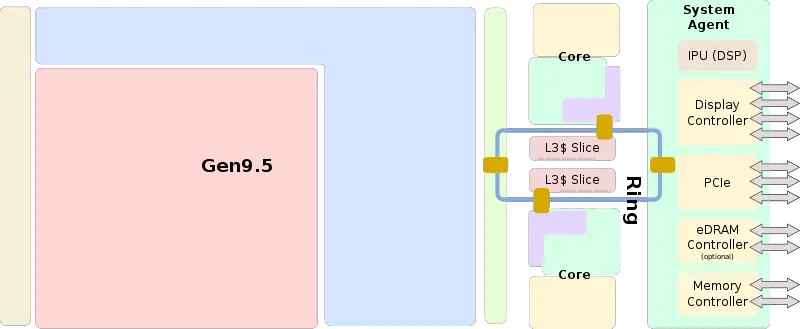
Entire SoC Overview (dual)[edit]
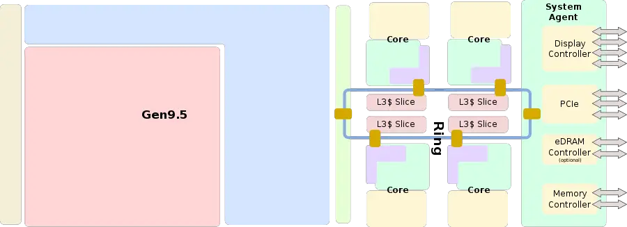
Entire SoC Overview (quad)[edit]
Individual Core[edit]
(Core identical to Skylake (client))
Gen9.5[edit]
See Gen9.5#Gen9.5.
Memory Hierarchy[edit]
The overall memory structure is identical to Skylake.
- Cache
- L0 µOP cache:
- 1,536 µOPs, 8-way set associative
- 32 sets, 6-µOP line size
- statically divided between threads, per core, inclusive with L1I
- 1,536 µOPs, 8-way set associative
- L1I Cache:
- 32 KiB, 8-way set associative
- 64 sets, 64 B line size
- shared by the two threads, per core
- 32 KiB, 8-way set associative
- L1D Cache:
- 32 KiB, 8-way set associative
- 64 sets, 64 B line size
- shared by the two threads, per core
- 4 cycles for fastest load-to-use (simple pointer accesses)
- 5 cycles for complex addresses
- 64 B/cycle load bandwidth
- 32 B/cycle store bandwidth
- Write-back policy
- L2 Cache:
- Unified, 256 KiB, 4-way set associative
- Non-inclusive
- 1024 sets, 64 B line size
- 12 cycles for fastest load-to-use
- 64 B/cycle bandwidth to L1$
- Write-back policy
- L3 Cache/LLC:
- Up to 2 MiB Per core, shared across all cores
- Up to 16-way set associative
- Inclusive
- 64 B line size
- Write-back policy
- Per each core:
- Read: 32 B/cycle (@ ring clock)
- Write: 32 B/cycle (@ ring clock)
- 42 cycles for fastest load-to-use
- Side Cache:
- System DRAM:
- 2 Channels
- 8 B/cycle/channel (@ memory clock)
- 42 cycles + 51 ns latency
- L0 µOP cache:
Kaby Lake TLB consists of dedicated L1 TLB for instruction cache (ITLB) and another one for data cache (DTLB). Additionally there is a unified L2 TLB (STLB).
- TLBs:
- ITLB
- 4 KiB page translations:
- 128 entries; 8-way set associative
- dynamic partitioning
- 2 MiB / 4 MiB page translations:
- 8 entries per thread; fully associative
- Duplicated for each thread
- 4 KiB page translations:
- DTLB
- 4 KiB page translations:
- 64 entries; 4-way set associative
- fixed partition
- 2 MiB / 4 MiB page translations:
- 32 entries; 4-way set associative
- fixed partition
- 1G page translations:
- 4 entries; 4-way set associative
- fixed partition
- 4 KiB page translations:
- STLB
- 4 KiB + 2 MiB page translations:
- 1536 entries; 12-way set associative
- fixed partition
- 1 GiB page translations:
- 16 entries; 4-way set associative
- fixed partition
- 4 KiB + 2 MiB page translations:
- ITLB
- Note: STLB is incorrectly reported as "6-way" by CPUID leaf 2 (EAX=02H). Kaby Lake erratum KBL096 recommends software to simply ignore that value.
Core[edit]
- Main article: Skylake § Core
Kaby Lake's core is identical to Skylake's.
Pipeline[edit]
- Main article: Skylake § Pipeline
Kaby Lake's pipeline is identical to Skylake's.
Configurability[edit]
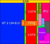
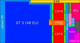
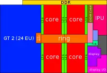
Kaby Lake builds upon the Skylake architecture, most dies are slight enhancements of their Skylake counterparts. The biggest change is the removal of the high performance quad core GT4 die, which has been replaced by the Kaby Lake G processors. And the introduction of the first low power quad core processor.
- Physical Layout Breakdown
Graphics[edit]
- Main article: Gen9.5
Support for three displays via HDMI 1.4[graphics 1], DisplayPort (DP) 1.2, and Embedded DisplayPort (eDP) 1.4 interfaces. Kaby Lake's biggest enhancement is the addition of native fixed function HEVC/VP9 decoding for 4K playback at 60fps (10-bit) as well as fixed function HEVC/VP9 encoding for 4K (8-bit).
| Integrated Graphics Processor | Standards | ||||||||||||
|---|---|---|---|---|---|---|---|---|---|---|---|---|---|
| Name | Execution Units | Tier | Series | eDRAM | Vulkan | Direct3D | OpenGL | OpenCL | |||||
| Windows | Linux | Windows | Linux | HLSL | Windows | Linux | Windows | Linux | |||||
| HD Graphics 610 | 12 | GT1 | S, U | - | 1.0 | 12 | N/A | 5.1 | 4.5 | 4.5 | 2.1 | 2.0 | |
| HD Graphics 615 | 24 | GT2 | Y | - | |||||||||
| HD Graphics 620 | 24 | GT2 | U, R | - | |||||||||
| HD Graphics 630 | 24 | GT2 | S, H | - | |||||||||
| HD Graphics P630 | 24 | GT2 | H | - | |||||||||
| Iris Plus Graphics 640 | 48 | GT3e | U | 64 MiB | |||||||||
| Iris Plus Graphics 650 | 48 | GT3e | U | 64 MiB | |||||||||
- ↑ Note that while there is no native HDMI 2.0 support, Intel did provide somewhat of an awkward solution using an LSPCON (Level Shifter/Protocol Converter) to drive DP to HDMI 1.4 signal + convert HDMI 1.4 to HDMI 2.0. One such solution is the MegaChips MCDP2800.
Hardware Accelerated Video[edit]
| [Edit] Kaby Lake (Gen9.5) Hardware Accelerated Video Capabilities | |||||||
|---|---|---|---|---|---|---|---|
| Codec | Encode | Decode | |||||
| Profiles | Levels | Max Resolution | Profiles | Levels | Max Resolution | ||
| MPEG-2 (H.262) | Main | High | 1080p (FHD) | Main | Main, High | 1080p (FHD) | |
| MPEG-4 AVC (H.264) | High, Main | 5.1 | 2160p (4K) | Main, High, MVC, Stereo | 5.1 | 2160p (4K) | |
| JPEG/MJPEG | Baseline | - | 16k x 16k | Baseline | Unified | 16k x 16k | |
| HEVC (H.265) | Main, Main 10 | 5.1 | 2160p (4K) | Main, Main 10 | 5.1 | 2160p (4K) | |
| VC-1 | ✘ | Advanced, Main, Simple | 3, High, Simple | 3840x3840 | |||
| VP8 | Unified | Unified | N/A | 0 | Unified | 1080p | |
| VP9 | 0 | 2160p (4K) | 0, 2 | Unified | 2160p (4K) | ||
Sockets/Platform[edit]
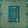
Kaby Lake Y and U are single-chip solutions. Y chips utilize a 2-die multi-chip package (MCP) whereas the Kaby Lake U's are either 2 or 3-die MCP configuration. The 3 die chip configuration are for the Iris IGPs which incorporate an on-package cache (OPC) in addition to the hub. Communication from the CPU to the hub on those chips are done via a lightweight On-Package Interconnect (OPI) interface. Kaby Lake S and H are a two-chip solution linked together via Intel's standard DMI 3.0 bus interface which utilizes 4 of the CPU's 20 PCIe 3.0 lanes (having a transfer rate of 8 GT/s per lane). Only Kaby Lake S (used on mainstream desktop processors) are not soldered onto the motherboard and can be interchanged/replaced.
| Core | Socket | Permanent | Platform | Chipset | Bus | |
|---|---|---|---|---|---|---|
 |
Kaby Lake Y | BGA-1515 | Yes | 1-chip | N/A | OPI |
 |
Kaby Lake U | BGA-1356 | Yes | 1-chip | ||
 |
Kaby Lake R | |||||
 |
Kaby Lake H | BGA-1440 | Yes | 2-chip | Sunrise Point[c 1] Union Point |
DMI 3.0 |
 |
Kaby Lake S | LGA-1151 | No | 2-chip | ||
| Kaby Lake DT | LGA-1151 | No | 2-chip | Xeon Sunrise Point Xeon Union Point | ||
 |
Kaby Lake X | LGA-2066 | No | 2-chip | Lewisburg |
- ↑ Requires a firmware update in order to work with Kaby Lake chips
Packages[edit]
| Core | Die Type | Package | Dimensions |
|---|---|---|---|
| Kaby Lake H | 4+2 | FCBGA-1440 | 42 mm x 28 mm x 1.46 mm |
| Kaby Lake H | 2+2 | ||
| Kaby Lake S | 4+2 | FCLGA-1151 | 37.5 mm x 37.5 mm x 4.4 mm |
| Kaby Lake S | 2+2 |
Clock domains[edit]
Kaby Lake is divided into a number of clock domains, each controlling the clock frequency of their respective unit in the processor. All clock domains are some multiple of the [virtual] bus clock (BCLK).
- BCLK - Bus/Base Clock - The system bus interface frequency (once upon a time referred to the actual FSB speed, it now serves as only a base clock reference for all other clock domains). The base clock is 100 MHz.
- Core Clock - The frequency at which the core and the L1/L2 caches operate at. (Frequency depends on the model and is represented as a multiple of BCLK).
- Ring Clock - The frequency at which the ring interconnect and LLC operate at. Data from/to the individual cores are read/written into the L3 at a rate of 32B/cycle operating at Ring Clock frequency.
- IGP Clock - The frequency at which the integrated graphics (Gen9 GPU) operates at. Data from/to the GPU are read/written into the LLC at a rate of 64B/cycle operating at this frequency as well.
- eDRAM Clock - The frequency at which the embedded DRAM operates at (only available for certain models). Data is read/written from/to the LLC at a rate of 32B/cycle operating at this frequency as well.
- MemClk - Memory Clock - The frequency at which the system DRAM operates at. DRAM data is transfered at a rate of 8B/cycle operating at MemClk frequency.
Overclocking[edit]
Kaby Lake G[edit]
- Main article: Kaby Lake G Core
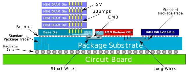
At CES 2018 (January 7) Intel announced 8th Gen Intel Core with Radeon RX Vega M, formerly code name Kaby Lake G. Those parts combine Intel's Kaby Lake H parts with and AMD Vega GPU as well as high-bandwidth memory 2.
All parts incorporate 4 GiB of HBM 2 along with an AMD Vega GPU. The HBM2 and GPU are interconnected using Intel's EMIB, however, the CPU and GPU are connected using standard in-package wires over standard PCIe 3.0. x8 lanes are permanently reserved for direct GPU-CPU communication. This leaves x8 additional lanes for all other peripherals that need direct connection to the CPU.
Intel claims that the use of HBM2 instead of GDDR5 results in 80% less power. It's worth noting that since those are Kaby Lake H parts with Radeon Graphics, they effectively have two GPUs and both GPUs are usable. Fairly significant power saving can be achieved by defaulting to the integrated graphics when high performance is not required. In total there are 3 display outputs from the integrated graphics and an additional 6 outputs from the Radeon graphics for a total of 9.
By moving from GDDR5 to HBM 2 and going to higher integration by packing everything into a single package, Intel has achieved considerably higher density. Intel reported that around 1900 mm² (~3 in²) board space saving has been achieved which is rather significant for ultra-light and ultra-thin notebooks and tablets where logic board area reduction is important. Additionally, this reduces the BOM for OEMs.
Dynamic Tuning[edit]
- Main article: Dynamic Tuning
With Kaby Lake G Intel introduced Dynamic Tuning which is a way of managing the entire package power consumption by adjusting the power policies of the GPU and CPU depending on the application. Applications that make no use of the discrete GPU will see the majority of the package power budget allocated for the CPU to accelerate that workloads while things like gaming will shift the power in favor of GPU acceleration. The feature is implemented entirely in software.
Graphics[edit]
Kaby Lake G has one of two possible AMD Radeon graphics based on the Vega microarchitecture.
| Radeon RX Vega | ||
|---|---|---|
| Graphics | Radeon RX Vega M GH | Radeon RX Vega M GL |
| Architecture | Vega M | Vega M |
| Compute Units | 24 | 20 |
| Stream Processors | 1,536 | 1,280 |
| ROPs | 64 pixels/clock | 32 pixels/clock |
| Base Clock | 1,063 MHz | 931 MHz |
| Boost Frequency | 1,190 MHz | 1,011 MHz |
| Peak Performance | 3.7 TFLOPS | 2.6 TFLOPS |
| HBM 2 | ||
| Capacity | 4 GiB | 4 GiB |
| Clock | 800 MHz | 700 MHz |
| Bandwidth | 204.8 GB/s | 179.2 GB/s |
Die[edit]
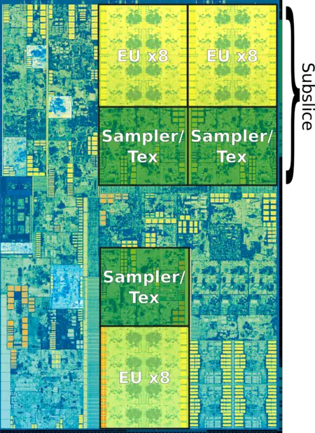
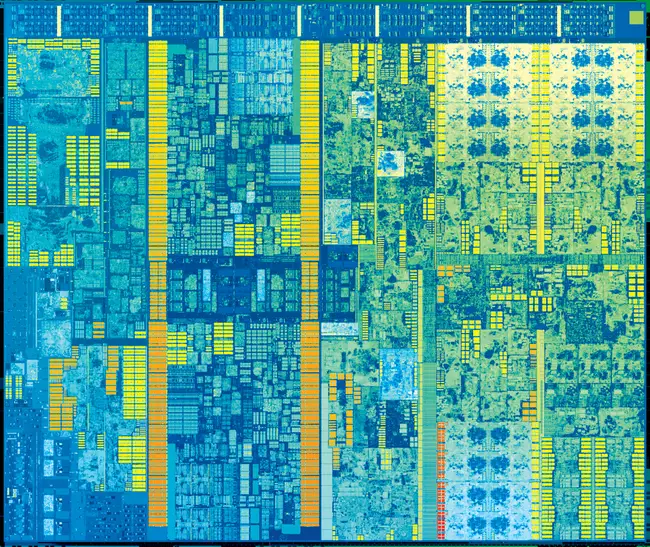
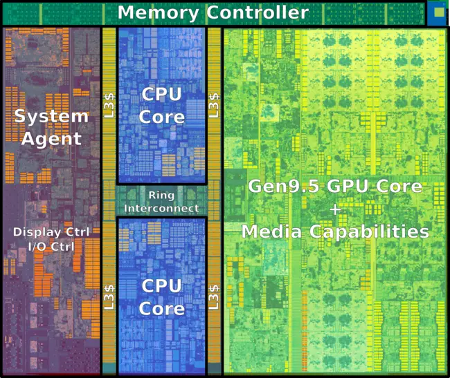
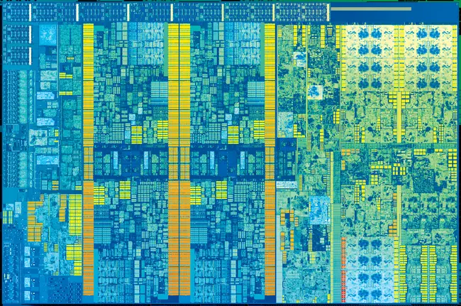
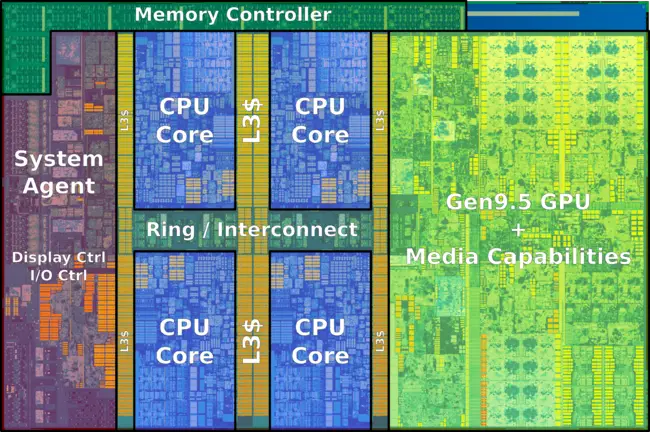
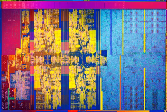
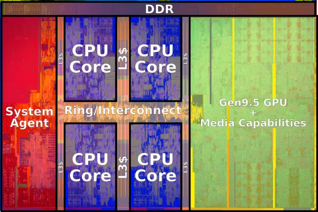
Kaby Lake desktop and mobile come and 2 and 4 cores. Each variant has its own die. One of the most noticeable changes on die is the amount of die space allocated to the GPU. The major components of the die are:
- System Agent
- CPU Core
- Ring bus interconnect
- Memory Controller
System Agent[edit]
The System Agent (SA) contains the Image Processing Unit (IPU), the Display Engine (DE), and the I/O bus. Note that the mainstream desktop (i.e., quad-core die) does not have an IPU (The memory controller actually occupies a portion of where it would otherwise be).
Integrated Graphics[edit]
The integrated graphics takes up the largest portion of the die. The normal dual-core and quad-core dies come with 24 EU Gen9.5 GPU (with 12 units disabled on the low end models).
Layout Difference from Skylake[edit]
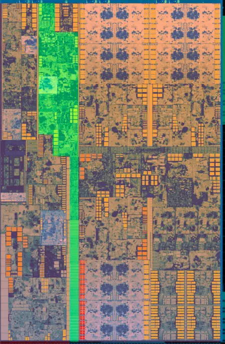
The majority of the enhancements to Kaby Lake comes from the Unslice portion of the Gen9.5 integrated GPU. The shaded region marked in green indicates new/modified physical layout changes. The rest of the die, shaded in red, is unchanged from Skylake.
Dual-Core[edit]
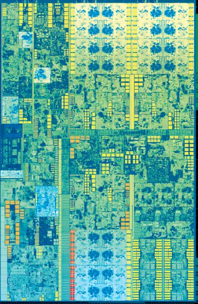
Die shot of the dual-core GT2 Kaby Lake processors. Those are found in mobile models, and entry-level/budget processors:
- 14 nm+ process
- 11 metal layers
- 2 CPU cores + 24 GPU EUs
Quad-Core[edit]
Die shot of the quad-core GT2 Kaby Lake processors. Those are found in almost all mainstream desktop processors.
- 14 nm+ process
- 11 metal layers
- ~9,21 mm x ~13,50 mm
- ~126 mm² die size
- 4 CPU cores + 24 GPU EUs
Quad-Core (Mobile Kaby Lake R)[edit]
With the introduction of Kaby Lake R, a new quad-core die was introduced. It's worth pointing out that this die is very different from the standard desktop quad-core die. Other than likely being optimized specifically for this market segment, this die also incorporates the IPU in the System Agent. Previously this integration was only found in the dual-core dies which were used for Skylake U and Kaby Lake U.
- 14 nm+ process
- 11 metal layers
- 123 mm² die size
- 4 CPU cores + 24 GPU EUs
Additional Shots[edit]
Additional die and wafer shots provided by Intel:
All Kaby Lake Chips[edit]
| Kaby Lake Chips | |||||||||||||||||||||||||
|---|---|---|---|---|---|---|---|---|---|---|---|---|---|---|---|---|---|---|---|---|---|---|---|---|---|
| Main processor | IGP | Major Feature Diff | |||||||||||||||||||||||
| Model | Launched | Price | Family | Platform | Core | Cores | Threads | L3$ | L4$ | TDP | Freq | Turbo | Max Mem | Name | Freq | Turbo | ECC | TBT | HT | AVX | AVX2 | TXT | TSX | vPro | VT-d |
| Uniprocessors | |||||||||||||||||||||||||
| 3865U | 3 January 2017 | Celeron | Kaby Lake | Kaby Lake U | 2 | 2 | 2 MiB 2,048 KiB 2,097,152 B 0.00195 GiB | 15 W 15,000 mW 0.0201 hp 0.015 kW | 1.8 GHz 1,800 MHz 1,800,000 kHz | 64 GiB 65,536 MiB 67,108,864 KiB 68,719,476,736 B 0.0625 TiB | HD Graphics 610 | 300 MHz 0.3 GHz 300,000 KHz | 900 MHz 0.9 GHz 900,000 KHz | ✘ | ✘ | ✘ | ✘ | ✘ | ✘ | ✘ | ✔ | ✔ | |||
| 3965U | 3 January 2017 | $ 107.00 € 96.30 £ 86.67 ¥ 11,056.31 | Celeron | Kaby Lake | Kaby Lake U | 2 | 2 | 2 MiB 2,048 KiB 2,097,152 B 0.00195 GiB | 15 W 15,000 mW 0.0201 hp 0.015 kW | 2.2 GHz 2,200 MHz 2,200,000 kHz | 64 GiB 65,536 MiB 67,108,864 KiB 68,719,476,736 B 0.0625 TiB | HD Graphics 610 | 300 MHz 0.3 GHz 300,000 KHz | 900 MHz 0.9 GHz 900,000 KHz | ✘ | ✘ | ✘ | ✘ | ✘ | ✘ | ✘ | ✔ | ✔ | ||
| 3965Y | Celeron | Kaby Lake | Kaby Lake Y | 2 | 2 | 2 MiB 2,048 KiB 2,097,152 B 0.00195 GiB | 6 W 6,000 mW 0.00805 hp 0.006 kW | 1.3 GHz 1,300 MHz 1,300,000 kHz | 16 GiB 16,384 MiB 16,777,216 KiB 17,179,869,184 B 0.0156 TiB | HD Graphics 615 | 300 MHz 0.3 GHz 300,000 KHz | 850 MHz 0.85 GHz 850,000 KHz | ✘ | ✘ | ✘ | ✘ | ✘ | ✘ | ✘ | ✔ | ✔ | ||||
| G3930 | 3 January 2017 | $ 42.00 € 37.80 £ 34.02 ¥ 4,339.86 | Celeron | Kaby Lake | Kaby Lake S | 2 | 2 | 2 MiB 2,048 KiB 2,097,152 B 0.00195 GiB | 51 W 51,000 mW 0.0684 hp 0.051 kW | 2.9 GHz 2,900 MHz 2,900,000 kHz | 64 GiB 65,536 MiB 67,108,864 KiB 68,719,476,736 B 0.0625 TiB | HD Graphics 610 | 350 MHz 0.35 GHz 350,000 KHz | 1,050 MHz 1.05 GHz 1,050,000 KHz | ✔ | ✘ | ✘ | ✘ | ✘ | ✘ | ✔ | ✘ | ✔ | ||
| G3930E | 12 June 2017 | $ 42.00 € 37.80 £ 34.02 ¥ 4,339.86 | Celeron | Kaby Lake | Kaby Lake S | 2 | 2 | 2 MiB 2,048 KiB 2,097,152 B 0.00195 GiB | 54 W 54,000 mW 0.0724 hp 0.054 kW | 2.9 GHz 2,900 MHz 2,900,000 kHz | 64 GiB 65,536 MiB 67,108,864 KiB 68,719,476,736 B 0.0625 TiB | HD Graphics 610 | 350 MHz 0.35 GHz 350,000 KHz | 1,000 MHz 1 GHz 1,000,000 KHz | ✔ | ✘ | ✘ | ✘ | ✘ | ✘ | ✔ | ✘ | ✔ | ||
| G3930T | 3 January 2017 | $ 42.00 € 37.80 £ 34.02 ¥ 4,339.86 | Celeron | Kaby Lake | Kaby Lake S | 2 | 2 | 2 MiB 2,048 KiB 2,097,152 B 0.00195 GiB | 35 W 35,000 mW 0.0469 hp 0.035 kW | 2.7 GHz 2,700 MHz 2,700,000 kHz | 64 GiB 65,536 MiB 67,108,864 KiB 68,719,476,736 B 0.0625 TiB | HD Graphics 610 | 350 MHz 0.35 GHz 350,000 KHz | 1,000 MHz 1 GHz 1,000,000 KHz | ✔ | ✘ | ✘ | ✘ | ✘ | ✘ | ✔ | ✘ | ✔ | ||
| G3930TE | 12 June 2017 | $ 42.00 € 37.80 £ 34.02 ¥ 4,339.86 | Celeron | Kaby Lake | Kaby Lake S | 2 | 2 | 2 MiB 2,048 KiB 2,097,152 B 0.00195 GiB | 35 W 35,000 mW 0.0469 hp 0.035 kW | 2.7 GHz 2,700 MHz 2,700,000 kHz | 64 GiB 65,536 MiB 67,108,864 KiB 68,719,476,736 B 0.0625 TiB | HD Graphics 610 | 350 MHz 0.35 GHz 350,000 KHz | 950 MHz 0.95 GHz 950,000 KHz | ✔ | ✘ | ✘ | ✘ | ✘ | ✘ | ✔ | ✘ | ✔ | ||
| G3950 | 3 January 2017 | $ 52.00 € 46.80 £ 42.12 ¥ 5,373.16 | Celeron | Kaby Lake | Kaby Lake S | 2 | 2 | 2 MiB 2,048 KiB 2,097,152 B 0.00195 GiB | 51 W 51,000 mW 0.0684 hp 0.051 kW | 3 GHz 3,000 MHz 3,000,000 kHz | 64 GiB 65,536 MiB 67,108,864 KiB 68,719,476,736 B 0.0625 TiB | HD Graphics 610 | 350 MHz 0.35 GHz 350,000 KHz | 1,050 MHz 1.05 GHz 1,050,000 KHz | ✔ | ✘ | ✘ | ✘ | ✘ | ✘ | ✔ | ✘ | ✔ | ||
| M3-7Y30 | 30 August 2016 | $ 281.00 € 252.90 £ 227.61 ¥ 29,035.73 | Core M3 | Kaby Lake | Kaby Lake Y | 2 | 4 | 4 MiB 4,096 KiB 4,194,304 B 0.00391 GiB | 4.5 W 4,500 mW 0.00603 hp 0.0045 kW | 1 GHz 1,000 MHz 1,000,000 kHz | 2.6 GHz 2,600 MHz 2,600,000 kHz | 16 GiB 16,384 MiB 16,777,216 KiB 17,179,869,184 B 0.0156 TiB | HD Graphics 615 | 300 MHz 0.3 GHz 300,000 KHz | 900 MHz 0.9 GHz 900,000 KHz | ✘ | ✔ | ✔ | ✔ | ✔ | ✘ | ✘ | ✘ | ✔ | |
| M3-7Y32 | 10 April 2017 | $ 281.00 € 252.90 £ 227.61 ¥ 29,035.73 | Core M3 | Kaby Lake | Kaby Lake Y | 2 | 4 | 4 MiB 4,096 KiB 4,194,304 B 0.00391 GiB | 4.5 W 4,500 mW 0.00603 hp 0.0045 kW | 1.1 GHz 1,100 MHz 1,100,000 kHz | 3 GHz 3,000 MHz 3,000,000 kHz | 16 GiB 16,384 MiB 16,777,216 KiB 17,179,869,184 B 0.0156 TiB | HD Graphics 615 | 300 MHz 0.3 GHz 300,000 KHz | 900 MHz 0.9 GHz 900,000 KHz | ✘ | ✔ | ✔ | ✔ | ✔ | ✘ | ✘ | ✘ | ✔ | |
| i3-7007U | Core i3 | Kaby Lake | Kaby Lake U | 2 | 4 | 3 MiB 3,072 KiB 3,145,728 B 0.00293 GiB | 15 W 15,000 mW 0.0201 hp 0.015 kW | 2.1 GHz 2,100 MHz 2,100,000 kHz | 32 GiB 32,768 MiB 33,554,432 KiB 34,359,738,368 B 0.0313 TiB | HD Graphics 620 | 300 MHz 0.3 GHz 300,000 KHz | 1,000 MHz 1 GHz 1,000,000 KHz | ✘ | ✘ | ✔ | ✔ | ✔ | ✘ | ✘ | ✘ | ✔ | ||||
| i3-7020U | 10 April 2018 | $ 281.00 € 252.90 £ 227.61 ¥ 29,035.73 | Core i3 | Kaby Lake | Kaby Lake U | 2 | 4 | 3 MiB 3,072 KiB 3,145,728 B 0.00293 GiB | 15 W 15,000 mW 0.0201 hp 0.015 kW | 2.3 GHz 2,300 MHz 2,300,000 kHz | 32 GiB 32,768 MiB 33,554,432 KiB 34,359,738,368 B 0.0313 TiB | HD Graphics 620 | 300 MHz 0.3 GHz 300,000 KHz | 1,000 MHz 1 GHz 1,000,000 KHz | ✘ | ✘ | ✔ | ✔ | ✔ | ✘ | ✘ | ✘ | ✔ | ||
| i3-7100 | 3 January 2017 | $ 117.00 € 105.30 £ 94.77 ¥ 12,089.61 | Core i3 | Kaby Lake | Kaby Lake S | 2 | 4 | 3 MiB 3,072 KiB 3,145,728 B 0.00293 GiB | 51 W 51,000 mW 0.0684 hp 0.051 kW | 3.9 GHz 3,900 MHz 3,900,000 kHz | 64 GiB 65,536 MiB 67,108,864 KiB 68,719,476,736 B 0.0625 TiB | HD Graphics 630 | 350 MHz 0.35 GHz 350,000 KHz | 1,100 MHz 1.1 GHz 1,100,000 KHz | ✔ | ✘ | ✔ | ✔ | ✔ | ✘ | ✔ | ✘ | ✘ | ||
| i3-7100E | 3 January 2017 | $ 225.00 € 202.50 £ 182.25 ¥ 23,249.25 | Core i3 | Kaby Lake | Kaby Lake H | 2 | 4 | 3 MiB 3,072 KiB 3,145,728 B 0.00293 GiB | 35 W 35,000 mW 0.0469 hp 0.035 kW | 2.9 GHz 2,900 MHz 2,900,000 kHz | 64 GiB 65,536 MiB 67,108,864 KiB 68,719,476,736 B 0.0625 TiB | HD Graphics 630 | 350 MHz 0.35 GHz 350,000 KHz | 950 MHz 0.95 GHz 950,000 KHz | ✔ | ✘ | ✔ | ✔ | ✔ | ✘ | ✘ | ✘ | ✔ | ||
| i3-7100H | 3 January 2017 | $ 225.00 € 202.50 £ 182.25 ¥ 23,249.25 | Core i3 | Kaby Lake | Kaby Lake H | 2 | 4 | 3 MiB 3,072 KiB 3,145,728 B 0.00293 GiB | 35 W 35,000 mW 0.0469 hp 0.035 kW | 3 GHz 3,000 MHz 3,000,000 kHz | 64 GiB 65,536 MiB 67,108,864 KiB 68,719,476,736 B 0.0625 TiB | HD Graphics 630 | 350 MHz 0.35 GHz 350,000 KHz | 950 MHz 0.95 GHz 950,000 KHz | ✘ | ✘ | ✔ | ✔ | ✔ | ✘ | ✘ | ✘ | ✔ | ||
| i3-7100T | 3 January 2017 | $ 117.00 € 105.30 £ 94.77 ¥ 12,089.61 | Core i3 | Kaby Lake | Kaby Lake S | 2 | 4 | 3 MiB 3,072 KiB 3,145,728 B 0.00293 GiB | 35 W 35,000 mW 0.0469 hp 0.035 kW | 3.4 GHz 3,400 MHz 3,400,000 kHz | 64 GiB 65,536 MiB 67,108,864 KiB 68,719,476,736 B 0.0625 TiB | HD Graphics 630 | 350 MHz 0.35 GHz 350,000 KHz | 1,100 MHz 1.1 GHz 1,100,000 KHz | ✘ | ✘ | ✔ | ✔ | ✔ | ✘ | ✔ | ✘ | ✘ | ||
| i3-7100U | 30 August 2016 | $ 281.00 € 252.90 £ 227.61 ¥ 29,035.73 | Core i3 | Kaby Lake | Kaby Lake U | 2 | 4 | 3 MiB 3,072 KiB 3,145,728 B 0.00293 GiB | 15 W 15,000 mW 0.0201 hp 0.015 kW | 2.4 GHz 2,400 MHz 2,400,000 kHz | 32 GiB 32,768 MiB 33,554,432 KiB 34,359,738,368 B 0.0313 TiB | HD Graphics 620 | 300 MHz 0.3 GHz 300,000 KHz | 1,000 MHz 1 GHz 1,000,000 KHz | ✘ | ✘ | ✔ | ✔ | ✔ | ✘ | ✘ | ✘ | ✔ | ||
| i3-7101E | 3 January 2017 | $ 117.00 € 105.30 £ 94.77 ¥ 12,089.61 | Core i3 | Kaby Lake | Kaby Lake S | 2 | 4 | 3 MiB 3,072 KiB 3,145,728 B 0.00293 GiB | 54 W 54,000 mW 0.0724 hp 0.054 kW | 3.9 GHz 3,900 MHz 3,900,000 kHz | 64 GiB 65,536 MiB 67,108,864 KiB 68,719,476,736 B 0.0625 TiB | HD Graphics 610 | 350 MHz 0.35 GHz 350,000 KHz | 1,100 MHz 1.1 GHz 1,100,000 KHz | ✔ | ✘ | ✔ | ✔ | ✔ | ✘ | ✘ | ✘ | ✔ | ||
| i3-7101TE | 3 January 2017 | $ 117.00 € 105.30 £ 94.77 ¥ 12,089.61 | Core i3 | Kaby Lake | Kaby Lake S | 2 | 4 | 3 MiB 3,072 KiB 3,145,728 B 0.00293 GiB | 35 W 35,000 mW 0.0469 hp 0.035 kW | 3.4 GHz 3,400 MHz 3,400,000 kHz | 64 GiB 65,536 MiB 67,108,864 KiB 68,719,476,736 B 0.0625 TiB | HD Graphics 610 | 350 MHz 0.35 GHz 350,000 KHz | 1,100 MHz 1.1 GHz 1,100,000 KHz | ✔ | ✘ | ✔ | ✔ | ✔ | ✘ | ✘ | ✘ | ✔ | ||
| i3-7102E | 3 January 2017 | $ 225.00 € 202.50 £ 182.25 ¥ 23,249.25 | Core i3 | Kaby Lake | Kaby Lake H | 2 | 4 | 3 MiB 3,072 KiB 3,145,728 B 0.00293 GiB | 25 W 25,000 mW 0.0335 hp 0.025 kW | 2.1 GHz 2,100 MHz 2,100,000 kHz | 64 GiB 65,536 MiB 67,108,864 KiB 68,719,476,736 B 0.0625 TiB | HD Graphics 630 | 350 MHz 0.35 GHz 350,000 KHz | 950 MHz 0.95 GHz 950,000 KHz | ✔ | ✘ | ✔ | ✔ | ✔ | ✘ | ✘ | ✘ | ✔ | ||
| i3-7110U | Core i3 | Kaby Lake | Kaby Lake U | 2 | 4 | 3 MiB 3,072 KiB 3,145,728 B 0.00293 GiB | 15 W 15,000 mW 0.0201 hp 0.015 kW | 2.6 GHz 2,600 MHz 2,600,000 kHz | 32 GiB 32,768 MiB 33,554,432 KiB 34,359,738,368 B 0.0313 TiB | HD Graphics 620 | 300 MHz 0.3 GHz 300,000 KHz | 1,000 MHz 1 GHz 1,000,000 KHz | ✘ | ✘ | ✔ | ✔ | ✔ | ✘ | ✘ | ✘ | ✔ | ||||
| i3-7120 | $ 117.00 € 105.30 £ 94.77 ¥ 12,089.61 | Core i3 | Kaby Lake | Kaby Lake S | 2 | 4 | 3 MiB 3,072 KiB 3,145,728 B 0.00293 GiB | 51 W 51,000 mW 0.0684 hp 0.051 kW | 4 GHz 4,000 MHz 4,000,000 kHz | 64 GiB 65,536 MiB 67,108,864 KiB 68,719,476,736 B 0.0625 TiB | HD Graphics 630 | 350 MHz 0.35 GHz 350,000 KHz | 1,100 MHz 1.1 GHz 1,100,000 KHz | ✘ | ✘ | ✔ | ✔ | ✔ | ✘ | ✔ | ✘ | ✘ | |||
| i3-7120T | $ 117.00 € 105.30 £ 94.77 ¥ 12,089.61 | Core i3 | Kaby Lake | Kaby Lake S | 2 | 4 | 3 MiB 3,072 KiB 3,145,728 B 0.00293 GiB | 35 W 35,000 mW 0.0469 hp 0.035 kW | 3.5 GHz 3,500 MHz 3,500,000 kHz | 64 GiB 65,536 MiB 67,108,864 KiB 68,719,476,736 B 0.0625 TiB | HD Graphics 630 | 350 MHz 0.35 GHz 350,000 KHz | 1,100 MHz 1.1 GHz 1,100,000 KHz | ✘ | ✘ | ✔ | ✔ | ✔ | ✘ | ✔ | ✘ | ✘ | |||
| i3-7130U | 12 June 2017 | Core i3 | Kaby Lake | Kaby Lake U | 2 | 4 | 3 MiB 3,072 KiB 3,145,728 B 0.00293 GiB | 15 W 15,000 mW 0.0201 hp 0.015 kW | 2.7 GHz 2,700 MHz 2,700,000 kHz | 32 GiB 32,768 MiB 33,554,432 KiB 34,359,738,368 B 0.0313 TiB | HD Graphics 620 | 300 MHz 0.3 GHz 300,000 KHz | 1,000 MHz 1 GHz 1,000,000 KHz | ✘ | ✘ | ✔ | ✔ | ✔ | ✘ | ✘ | ✘ | ✔ | |||
| i3-7167U | 3 January 2017 | $ 304.00 € 273.60 £ 246.24 ¥ 31,412.32 | Core i3 | Kaby Lake | Kaby Lake U | 2 | 4 | 3 MiB 3,072 KiB 3,145,728 B 0.00293 GiB | 64 MiB 65,536 KiB 67,108,864 B 0.0625 GiB | 28 W 28,000 mW 0.0375 hp 0.028 kW | 2.8 GHz 2,800 MHz 2,800,000 kHz | 32 GiB 32,768 MiB 33,554,432 KiB 34,359,738,368 B 0.0313 TiB | Iris Plus Graphics 650 | 300 MHz 0.3 GHz 300,000 KHz | 1,000 MHz 1 GHz 1,000,000 KHz | ✘ | ✘ | ✔ | ✔ | ✔ | ✘ | ✘ | ✘ | ✔ | |
| i3-7300 | 3 January 2017 | $ 147.00 € 132.30 £ 119.07 ¥ 15,189.51 | Core i3 | Kaby Lake | Kaby Lake S | 2 | 4 | 4 MiB 4,096 KiB 4,194,304 B 0.00391 GiB | 51 W 51,000 mW 0.0684 hp 0.051 kW | 4 GHz 4,000 MHz 4,000,000 kHz | 64 GiB 65,536 MiB 67,108,864 KiB 68,719,476,736 B 0.0625 TiB | HD Graphics 630 | 350 MHz 0.35 GHz 350,000 KHz | 1,150 MHz 1.15 GHz 1,150,000 KHz | ✘ | ✘ | ✔ | ✔ | ✔ | ✘ | ✔ | ✘ | ✘ | ||
| i3-7300T | 3 January 2017 | $ 147.00 € 132.30 £ 119.07 ¥ 15,189.51 | Core i3 | Kaby Lake | Kaby Lake S | 2 | 4 | 4 MiB 4,096 KiB 4,194,304 B 0.00391 GiB | 35 W 35,000 mW 0.0469 hp 0.035 kW | 3.5 GHz 3,500 MHz 3,500,000 kHz | 64 GiB 65,536 MiB 67,108,864 KiB 68,719,476,736 B 0.0625 TiB | HD Graphics 630 | 350 MHz 0.35 GHz 350,000 KHz | 1,100 MHz 1.1 GHz 1,100,000 KHz | ✘ | ✘ | ✔ | ✔ | ✔ | ✘ | ✔ | ✘ | ✘ | ||
| i3-7310T | 2017 | Core i3 | Kaby Lake | Kaby Lake S | 2 | 4 | 4 MiB 4,096 KiB 4,194,304 B 0.00391 GiB | 35 W 35,000 mW 0.0469 hp 0.035 kW | 3.4 GHz 3,400 MHz 3,400,000 kHz | 64 GiB 65,536 MiB 67,108,864 KiB 68,719,476,736 B 0.0625 TiB | HD Graphics 630 | 350 MHz 0.35 GHz 350,000 KHz | 1,100 MHz 1.1 GHz 1,100,000 KHz | ✘ | ✘ | ✔ | ✔ | ✔ | ✘ | ✔ | ✘ | ✘ | |||
| i3-7310U | Core i3 | Kaby Lake | Kaby Lake U | 2 | 4 | 3 MiB 3,072 KiB 3,145,728 B 0.00293 GiB | 15 W 15,000 mW 0.0201 hp 0.015 kW | 2.7 GHz 2,700 MHz 2,700,000 kHz | 32 GiB 32,768 MiB 33,554,432 KiB 34,359,738,368 B 0.0313 TiB | HD Graphics 620 | 300 MHz 0.3 GHz 300,000 KHz | 1,000 MHz 1 GHz 1,000,000 KHz | ✘ | ✘ | ✔ | ✔ | ✔ | ✘ | ✘ | ✘ | ✔ | ||||
| i3-7320 | 3 January 2017 | $ 157.00 € 141.30 £ 127.17 ¥ 16,222.81 | Core i3 | Kaby Lake | Kaby Lake S | 2 | 4 | 4 MiB 4,096 KiB 4,194,304 B 0.00391 GiB | 51 W 51,000 mW 0.0684 hp 0.051 kW | 4.1 GHz 4,100 MHz 4,100,000 kHz | 64 GiB 65,536 MiB 67,108,864 KiB 68,719,476,736 B 0.0625 TiB | HD Graphics 630 | 350 MHz 0.35 GHz 350,000 KHz | 1,150 MHz 1.15 GHz 1,150,000 KHz | ✘ | ✘ | ✔ | ✔ | ✔ | ✘ | ✔ | ✘ | ✘ | ||
| i3-7320T | $ 147.00 € 132.30 £ 119.07 ¥ 15,189.51 | Core i3 | Kaby Lake | Kaby Lake S | 2 | 4 | 4 MiB 4,096 KiB 4,194,304 B 0.00391 GiB | 35 W 35,000 mW 0.0469 hp 0.035 kW | 3.6 GHz 3,600 MHz 3,600,000 kHz | 64 GiB 65,536 MiB 67,108,864 KiB 68,719,476,736 B 0.0625 TiB | HD Graphics 630 | 350 MHz 0.35 GHz 350,000 KHz | 1,100 MHz 1.1 GHz 1,100,000 KHz | ✘ | ✘ | ✔ | ✔ | ✔ | ✘ | ✔ | ✘ | ✘ | |||
| i3-7340 | $ 157.00 € 141.30 £ 127.17 ¥ 16,222.81 | Core i3 | Kaby Lake | Kaby Lake S | 2 | 4 | 4 MiB 4,096 KiB 4,194,304 B 0.00391 GiB | 51 W 51,000 mW 0.0684 hp 0.051 kW | 4.2 GHz 4,200 MHz 4,200,000 kHz | 64 GiB 65,536 MiB 67,108,864 KiB 68,719,476,736 B 0.0625 TiB | HD Graphics 630 | 350 MHz 0.35 GHz 350,000 KHz | 1,150 MHz 1.15 GHz 1,150,000 KHz | ✘ | ✘ | ✔ | ✔ | ✔ | ✘ | ✔ | ✘ | ✘ | |||
| i3-7350K | 3 January 2017 | $ 179.00 € 161.10 £ 144.99 ¥ 18,496.07 | Core i3 | Kaby Lake | Kaby Lake S | 2 | 4 | 4 MiB 4,096 KiB 4,194,304 B 0.00391 GiB | 60 W 60,000 mW 0.0805 hp 0.06 kW | 4.2 GHz 4,200 MHz 4,200,000 kHz | 64 GiB 65,536 MiB 67,108,864 KiB 68,719,476,736 B 0.0625 TiB | HD Graphics 630 | 350 MHz 0.35 GHz 350,000 KHz | 1,150 MHz 1.15 GHz 1,150,000 KHz | ✘ | ✘ | ✔ | ✔ | ✔ | ✘ | ✔ | ✘ | ✘ | ||
| i3-8130U | 12 February 2018 | $ 281.00 € 252.90 £ 227.61 ¥ 29,035.73 | Core i3 | Kaby Lake U | 2 | 4 | 4 MiB 4,096 KiB 4,194,304 B 0.00391 GiB | 15 W 15,000 mW 0.0201 hp 0.015 kW | 2.2 GHz 2,200 MHz 2,200,000 kHz | 3.4 GHz 3,400 MHz 3,400,000 kHz | 32 GiB 32,768 MiB 33,554,432 KiB 34,359,738,368 B 0.0313 TiB | UHD Graphics 620 | 300 MHz 0.3 GHz 300,000 KHz | 1,000 MHz 1 GHz 1,000,000 KHz | ✘ | ✘ | ✔ | ✔ | ✔ | ✘ | ✘ | ✘ | ✔ | ||
| i5-7200U | 30 August 2016 | $ 281.00 € 252.90 £ 227.61 ¥ 29,035.73 | Core i5 | Kaby Lake | Kaby Lake U | 2 | 4 | 3 MiB 3,072 KiB 3,145,728 B 0.00293 GiB | 15 W 15,000 mW 0.0201 hp 0.015 kW | 2.5 GHz 2,500 MHz 2,500,000 kHz | 3.1 GHz 3,100 MHz 3,100,000 kHz | 32 GiB 32,768 MiB 33,554,432 KiB 34,359,738,368 B 0.0313 TiB | HD Graphics 620 | 300 MHz 0.3 GHz 300,000 KHz | 1,000 MHz 1 GHz 1,000,000 KHz | ✘ | ✔ | ✔ | ✔ | ✔ | ✘ | ✘ | ✘ | ✔ | |
| i5-7210U | Core i5 | Kaby Lake | Kaby Lake U | 2 | 4 | 3 MiB 3,072 KiB 3,145,728 B 0.00293 GiB | 15 W 15,000 mW 0.0201 hp 0.015 kW | 2.5 GHz 2,500 MHz 2,500,000 kHz | 3.3 GHz 3,300 MHz 3,300,000 kHz | 32 GiB 32,768 MiB 33,554,432 KiB 34,359,738,368 B 0.0313 TiB | HD Graphics 620 | 300 MHz 0.3 GHz 300,000 KHz | 1,000 MHz 1 GHz 1,000,000 KHz | ✘ | ✔ | ✔ | ✔ | ✔ | ✘ | ✘ | ✘ | ✔ | |||
| i5-7260U | 3 January 2017 | $ 304.00 € 273.60 £ 246.24 ¥ 31,412.32 | Core i5 | Kaby Lake | Kaby Lake U | 2 | 4 | 4 MiB 4,096 KiB 4,194,304 B 0.00391 GiB | 64 MiB 65,536 KiB 67,108,864 B 0.0625 GiB | 15 W 15,000 mW 0.0201 hp 0.015 kW | 2.2 GHz 2,200 MHz 2,200,000 kHz | 3.4 GHz 3,400 MHz 3,400,000 kHz | 32 GiB 32,768 MiB 33,554,432 KiB 34,359,738,368 B 0.0313 TiB | Iris Plus Graphics 640 | 300 MHz 0.3 GHz 300,000 KHz | 950 MHz 0.95 GHz 950,000 KHz | ✘ | ✔ | ✔ | ✔ | ✔ | ✘ | ✘ | ✘ | ✔ |
| i5-7267U | 3 January 2017 | $ 304.00 € 273.60 £ 246.24 ¥ 31,412.32 | Core i5 | Kaby Lake | Kaby Lake U | 2 | 4 | 4 MiB 4,096 KiB 4,194,304 B 0.00391 GiB | 64 MiB 65,536 KiB 67,108,864 B 0.0625 GiB | 28 W 28,000 mW 0.0375 hp 0.028 kW | 3.1 GHz 3,100 MHz 3,100,000 kHz | 3.5 GHz 3,500 MHz 3,500,000 kHz | 32 GiB 32,768 MiB 33,554,432 KiB 34,359,738,368 B 0.0313 TiB | Iris Plus Graphics 650 | 300 MHz 0.3 GHz 300,000 KHz | 1,050 MHz 1.05 GHz 1,050,000 KHz | ✘ | ✔ | ✔ | ✔ | ✔ | ✘ | ✘ | ✘ | ✔ |
| i5-7287U | 3 January 2017 | $ 304.00 € 273.60 £ 246.24 ¥ 31,412.32 | Core i5 | Kaby Lake | Kaby Lake U | 2 | 4 | 4 MiB 4,096 KiB 4,194,304 B 0.00391 GiB | 64 MiB 65,536 KiB 67,108,864 B 0.0625 GiB | 28 W 28,000 mW 0.0375 hp 0.028 kW | 3.3 GHz 3,300 MHz 3,300,000 kHz | 3.7 GHz 3,700 MHz 3,700,000 kHz | 32 GiB 32,768 MiB 33,554,432 KiB 34,359,738,368 B 0.0313 TiB | Iris Plus Graphics 650 | 300 MHz 0.3 GHz 300,000 KHz | 1,100 MHz 1.1 GHz 1,100,000 KHz | ✘ | ✔ | ✔ | ✔ | ✔ | ✘ | ✘ | ✘ | ✔ |
| i5-7300HQ | 3 January 2017 | $ 250.00 € 225.00 £ 202.50 ¥ 25,832.50 | Core i5 | Kaby Lake | Kaby Lake H | 4 | 4 | 6 MiB 6,144 KiB 6,291,456 B 0.00586 GiB | 45 W 45,000 mW 0.0603 hp 0.045 kW | 2.5 GHz 2,500 MHz 2,500,000 kHz | 3.5 GHz 3,500 MHz 3,500,000 kHz | 64 GiB 65,536 MiB 67,108,864 KiB 68,719,476,736 B 0.0625 TiB | HD Graphics 630 | 350 MHz 0.35 GHz 350,000 KHz | 1,000 MHz 1 GHz 1,000,000 KHz | ✘ | ✔ | ✘ | ✔ | ✔ | ✘ | ✔ | ✘ | ✔ | |
| i5-7300U | 3 January 2017 | $ 281.00 € 252.90 £ 227.61 ¥ 29,035.73 | Core i5 | Kaby Lake | Kaby Lake U | 2 | 4 | 3 MiB 3,072 KiB 3,145,728 B 0.00293 GiB | 15 W 15,000 mW 0.0201 hp 0.015 kW | 2.6 GHz 2,600 MHz 2,600,000 kHz | 3.5 GHz 3,500 MHz 3,500,000 kHz | 32 GiB 32,768 MiB 33,554,432 KiB 34,359,738,368 B 0.0313 TiB | HD Graphics 620 | 300 MHz 0.3 GHz 300,000 KHz | 1,100 MHz 1.1 GHz 1,100,000 KHz | ✔ | ✔ | ✔ | ✔ | ✔ | ✔ | ✔ | ✔ | ✔ | |
| i5-7360U | 3 January 2017 | $ 304.00 € 273.60 £ 246.24 ¥ 31,412.32 | Core i5 | Kaby Lake | Kaby Lake U | 2 | 4 | 4 MiB 4,096 KiB 4,194,304 B 0.00391 GiB | 64 MiB 65,536 KiB 67,108,864 B 0.0625 GiB | 15 W 15,000 mW 0.0201 hp 0.015 kW | 2.3 GHz 2,300 MHz 2,300,000 kHz | 3.6 GHz 3,600 MHz 3,600,000 kHz | 32 GiB 32,768 MiB 33,554,432 KiB 34,359,738,368 B 0.0313 TiB | Iris Plus Graphics 640 | 300 MHz 0.3 GHz 300,000 KHz | 1,000 MHz 1 GHz 1,000,000 KHz | ✘ | ✔ | ✔ | ✔ | ✔ | ✔ | ✔ | ✔ | ✔ |
| i5-7400 | 3 January 2017 | $ 182.00 € 163.80 £ 147.42 ¥ 18,806.06 | Core i5 | Kaby Lake | Kaby Lake S | 4 | 4 | 6 MiB 6,144 KiB 6,291,456 B 0.00586 GiB | 65 W 65,000 mW 0.0872 hp 0.065 kW | 3 GHz 3,000 MHz 3,000,000 kHz | 3.5 GHz 3,500 MHz 3,500,000 kHz | 64 GiB 65,536 MiB 67,108,864 KiB 68,719,476,736 B 0.0625 TiB | HD Graphics 630 | 350 MHz 0.35 GHz 350,000 KHz | 1,000 MHz 1 GHz 1,000,000 KHz | ✘ | ✔ | ✘ | ✔ | ✔ | ✘ | ✔ | ✘ | ✔ | |
| i5-7400T | 3 January 2017 | $ 187.00 € 168.30 £ 151.47 ¥ 19,322.71 | Core i5 | Kaby Lake | Kaby Lake S | 4 | 4 | 6 MiB 6,144 KiB 6,291,456 B 0.00586 GiB | 35 W 35,000 mW 0.0469 hp 0.035 kW | 2.4 GHz 2,400 MHz 2,400,000 kHz | 3 GHz 3,000 MHz 3,000,000 kHz | 64 GiB 65,536 MiB 67,108,864 KiB 68,719,476,736 B 0.0625 TiB | HD Graphics 630 | 350 MHz 0.35 GHz 350,000 KHz | 1,000 MHz 1 GHz 1,000,000 KHz | ✘ | ✔ | ✘ | ✔ | ✔ | ✘ | ✔ | ✘ | ✔ | |
| i5-7440EQ | 3 January 2017 | $ 250.00 € 225.00 £ 202.50 ¥ 25,832.50 | Core i5 | Kaby Lake | Kaby Lake H | 4 | 4 | 6 MiB 6,144 KiB 6,291,456 B 0.00586 GiB | 45 W 45,000 mW 0.0603 hp 0.045 kW | 2.9 GHz 2,900 MHz 2,900,000 kHz | 3.6 GHz 3,600 MHz 3,600,000 kHz | 64 GiB 65,536 MiB 67,108,864 KiB 68,719,476,736 B 0.0625 TiB | HD Graphics 630 | 350 MHz 0.35 GHz 350,000 KHz | 1,000 MHz 1 GHz 1,000,000 KHz | ✘ | ✔ | ✘ | ✔ | ✔ | ✔ | ✔ | ✔ | ✔ | |
| i5-7440HQ | 3 January 2017 | $ 250.00 € 225.00 £ 202.50 ¥ 25,832.50 | Core i5 | Kaby Lake | Kaby Lake H | 4 | 4 | 6 MiB 6,144 KiB 6,291,456 B 0.00586 GiB | 45 W 45,000 mW 0.0603 hp 0.045 kW | 2.8 GHz 2,800 MHz 2,800,000 kHz | 3.8 GHz 3,800 MHz 3,800,000 kHz | 64 GiB 65,536 MiB 67,108,864 KiB 68,719,476,736 B 0.0625 TiB | HD Graphics 630 | 350 MHz 0.35 GHz 350,000 KHz | 1,000 MHz 1 GHz 1,000,000 KHz | ✘ | ✔ | ✘ | ✔ | ✔ | ✔ | ✔ | ✔ | ✔ | |
| i5-7442EQ | 3 January 2017 | $ 250.00 € 225.00 £ 202.50 ¥ 25,832.50 | Core i5 | Kaby Lake | Kaby Lake H | 4 | 4 | 6 MiB 6,144 KiB 6,291,456 B 0.00586 GiB | 25 W 25,000 mW 0.0335 hp 0.025 kW | 2.1 GHz 2,100 MHz 2,100,000 kHz | 2.9 GHz 2,900 MHz 2,900,000 kHz | 64 GiB 65,536 MiB 67,108,864 KiB 68,719,476,736 B 0.0625 TiB | HD Graphics 630 | 350 MHz 0.35 GHz 350,000 KHz | 1,000 MHz 1 GHz 1,000,000 KHz | ✘ | ✔ | ✘ | ✔ | ✔ | ✔ | ✔ | ✔ | ✔ | |
| i5-7500 | 3 January 2017 | $ 202.00 € 181.80 £ 163.62 ¥ 20,872.66 | Core i5 | Kaby Lake | Kaby Lake S | 4 | 4 | 6 MiB 6,144 KiB 6,291,456 B 0.00586 GiB | 65 W 65,000 mW 0.0872 hp 0.065 kW | 3.4 GHz 3,400 MHz 3,400,000 kHz | 3.8 GHz 3,800 MHz 3,800,000 kHz | 64 GiB 65,536 MiB 67,108,864 KiB 68,719,476,736 B 0.0625 TiB | HD Graphics 630 | 350 MHz 0.35 GHz 350,000 KHz | 1,100 MHz 1.1 GHz 1,100,000 KHz | ✘ | ✔ | ✘ | ✔ | ✔ | ✔ | ✔ | ✔ | ✔ | |
| i5-7500T | 3 January 2017 | $ 202.00 € 181.80 £ 163.62 ¥ 20,872.66 | Core i5 | Kaby Lake | Kaby Lake S | 4 | 4 | 6 MiB 6,144 KiB 6,291,456 B 0.00586 GiB | 35 W 35,000 mW 0.0469 hp 0.035 kW | 2.7 GHz 2,700 MHz 2,700,000 kHz | 3.3 GHz 3,300 MHz 3,300,000 kHz | 64 GiB 65,536 MiB 67,108,864 KiB 68,719,476,736 B 0.0625 TiB | HD Graphics 630 | 350 MHz 0.35 GHz 350,000 KHz | 1,100 MHz 1.1 GHz 1,100,000 KHz | ✘ | ✔ | ✘ | ✔ | ✔ | ✔ | ✔ | ✔ | ✔ | |
| i5-7600 | 3 January 2017 | $ 224.00 € 201.60 £ 181.44 ¥ 23,145.92 | Core i5 | Kaby Lake | Kaby Lake S | 4 | 4 | 6 MiB 6,144 KiB 6,291,456 B 0.00586 GiB | 65 W 65,000 mW 0.0872 hp 0.065 kW | 3.5 GHz 3,500 MHz 3,500,000 kHz | 4.1 GHz 4,100 MHz 4,100,000 kHz | 64 GiB 65,536 MiB 67,108,864 KiB 68,719,476,736 B 0.0625 TiB | HD Graphics 630 | 350 MHz 0.35 GHz 350,000 KHz | 1,150 MHz 1.15 GHz 1,150,000 KHz | ✘ | ✔ | ✘ | ✔ | ✔ | ✔ | ✔ | ✔ | ✔ | |
| i5-7600K | 3 January 2017 | $ 243.00 € 218.70 £ 196.83 ¥ 25,109.19 | Core i5 | Kaby Lake | Kaby Lake S | 4 | 4 | 6 MiB 6,144 KiB 6,291,456 B 0.00586 GiB | 91 W 91,000 mW 0.122 hp 0.091 kW | 3.8 GHz 3,800 MHz 3,800,000 kHz | 4.2 GHz 4,200 MHz 4,200,000 kHz | 64 GiB 65,536 MiB 67,108,864 KiB 68,719,476,736 B 0.0625 TiB | HD Graphics 630 | 350 MHz 0.35 GHz 350,000 KHz | 1,150 MHz 1.15 GHz 1,150,000 KHz | ✘ | ✔ | ✘ | ✔ | ✔ | ✘ | ✔ | ✘ | ✔ | |
| i5-7600T | 3 January 2017 | $ 224.00 € 201.60 £ 181.44 ¥ 23,145.92 | Core i5 | Kaby Lake | Kaby Lake S | 4 | 4 | 6 MiB 6,144 KiB 6,291,456 B 0.00586 GiB | 35 W 35,000 mW 0.0469 hp 0.035 kW | 2.8 GHz 2,800 MHz 2,800,000 kHz | 3.7 GHz 3,700 MHz 3,700,000 kHz | 64 GiB 65,536 MiB 67,108,864 KiB 68,719,476,736 B 0.0625 TiB | HD Graphics 630 | 350 MHz 0.35 GHz 350,000 KHz | 1,100 MHz 1.1 GHz 1,100,000 KHz | ✘ | ✔ | ✘ | ✔ | ✔ | ✔ | ✔ | ✔ | ✔ | |
| i5-7640X | 26 June 2017 | $ 242.00 € 217.80 £ 196.02 ¥ 25,005.86 | Core i5 | Basin Falls | Kaby Lake X | 4 | 4 | 6 MiB 6,144 KiB 6,291,456 B 0.00586 GiB | 112 W 112,000 mW 0.15 hp 0.112 kW | 4 GHz 4,000 MHz 4,000,000 kHz | 4.2 GHz 4,200 MHz 4,200,000 kHz | 64 GiB 65,536 MiB 67,108,864 KiB 68,719,476,736 B 0.0625 TiB | ✘ | ✔ | ✘ | ✔ | ✔ | ✘ | ✔ | ✘ | ✔ | ||||
| i5-7Y54 | 30 August 2016 | $ 281.00 € 252.90 £ 227.61 ¥ 29,035.73 | Core i5 | Kaby Lake | Kaby Lake Y | 2 | 4 | 4 MiB 4,096 KiB 4,194,304 B 0.00391 GiB | 4.5 W 4,500 mW 0.00603 hp 0.0045 kW | 1.2 GHz 1,200 MHz 1,200,000 kHz | 3.2 GHz 3,200 MHz 3,200,000 kHz | 16 GiB 16,384 MiB 16,777,216 KiB 17,179,869,184 B 0.0156 TiB | HD Graphics 615 | 300 MHz 0.3 GHz 300,000 KHz | 950 MHz 0.95 GHz 950,000 KHz | ✘ | ✔ | ✔ | ✔ | ✔ | ✘ | ✘ | ✘ | ✔ | |
| i5-7Y57 | 3 January 2017 | $ 281.00 € 252.90 £ 227.61 ¥ 29,035.73 | Core i5 | Kaby Lake | Kaby Lake Y | 2 | 4 | 4 MiB 4,096 KiB 4,194,304 B 0.00391 GiB | 4.5 W 4,500 mW 0.00603 hp 0.0045 kW | 1.2 GHz 1,200 MHz 1,200,000 kHz | 3.3 GHz 3,300 MHz 3,300,000 kHz | 16 GiB 16,384 MiB 16,777,216 KiB 17,179,869,184 B 0.0156 TiB | HD Graphics 615 | 300 MHz 0.3 GHz 300,000 KHz | 950 MHz 0.95 GHz 950,000 KHz | ✘ | ✔ | ✔ | ✔ | ✔ | ✔ | ✔ | ✔ | ✔ | |
| i7-7510U | Core i7 | Kaby Lake | Kaby Lake U | 2 | 4 | 4 MiB 4,096 KiB 4,194,304 B 0.00391 GiB | 15 W 15,000 mW 0.0201 hp 0.015 kW | 2.7 GHz 2,700 MHz 2,700,000 kHz | 3.7 GHz 3,700 MHz 3,700,000 kHz | 32 GiB 32,768 MiB 33,554,432 KiB 34,359,738,368 B 0.0313 TiB | HD Graphics 620 | 300 MHz 0.3 GHz 300,000 KHz | 1,150 MHz 1.15 GHz 1,150,000 KHz | ✘ | ✔ | ✔ | ✔ | ✔ | ✘ | ✘ | ✘ | ✔ | |||
| i7-7560U | 3 January 2017 | $ 415.00 € 373.50 £ 336.15 ¥ 42,881.95 | Core i7 | Kaby Lake | Kaby Lake U | 2 | 4 | 4 MiB 4,096 KiB 4,194,304 B 0.00391 GiB | 64 MiB 65,536 KiB 67,108,864 B 0.0625 GiB | 15 W 15,000 mW 0.0201 hp 0.015 kW | 2.4 GHz 2,400 MHz 2,400,000 kHz | 3.8 GHz 3,800 MHz 3,800,000 kHz | 32 GiB 32,768 MiB 33,554,432 KiB 34,359,738,368 B 0.0313 TiB | Iris Plus Graphics 640 | 300 MHz 0.3 GHz 300,000 KHz | 1,050 MHz 1.05 GHz 1,050,000 KHz | ✘ | ✔ | ✔ | ✔ | ✔ | ✘ | ✘ | ✘ | ✔ |
| i7-7567U | 3 January 2017 | $ 415.00 € 373.50 £ 336.15 ¥ 42,881.95 | Core i7 | Kaby Lake | Kaby Lake U | 2 | 4 | 4 MiB 4,096 KiB 4,194,304 B 0.00391 GiB | 64 MiB 65,536 KiB 67,108,864 B 0.0625 GiB | 28 W 28,000 mW 0.0375 hp 0.028 kW | 3.5 GHz 3,500 MHz 3,500,000 kHz | 4 GHz 4,000 MHz 4,000,000 kHz | 16 GiB 16,384 MiB 16,777,216 KiB 17,179,869,184 B 0.0156 TiB | Iris Plus Graphics 650 | 300 MHz 0.3 GHz 300,000 KHz | 1,150 MHz 1.15 GHz 1,150,000 KHz | ✘ | ✔ | ✔ | ✔ | ✔ | ✘ | ✘ | ✘ | ✔ |
| i7-7600U | 3 January 2017 | $ 393.00 € 353.70 £ 318.33 ¥ 40,608.69 | Core i7 | Kaby Lake | Kaby Lake U | 2 | 4 | 4 MiB 4,096 KiB 4,194,304 B 0.00391 GiB | 15 W 15,000 mW 0.0201 hp 0.015 kW | 2.8 GHz 2,800 MHz 2,800,000 kHz | 3.9 GHz 3,900 MHz 3,900,000 kHz | 32 GiB 32,768 MiB 33,554,432 KiB 34,359,738,368 B 0.0313 TiB | HD Graphics 620 | 300 MHz 0.3 GHz 300,000 KHz | 1,150 MHz 1.15 GHz 1,150,000 KHz | ✘ | ✔ | ✔ | ✔ | ✔ | ✔ | ✔ | ✔ | ✔ | |
| i7-7660U | 3 January 2017 | $ 415.00 € 373.50 £ 336.15 ¥ 42,881.95 | Core i7 | Kaby Lake | Kaby Lake U | 2 | 4 | 4 MiB 4,096 KiB 4,194,304 B 0.00391 GiB | 64 MiB 65,536 KiB 67,108,864 B 0.0625 GiB | 15 W 15,000 mW 0.0201 hp 0.015 kW | 2.5 GHz 2,500 MHz 2,500,000 kHz | 4 GHz 4,000 MHz 4,000,000 kHz | 32 GiB 32,768 MiB 33,554,432 KiB 34,359,738,368 B 0.0313 TiB | Iris Plus Graphics 640 | 300 MHz 0.3 GHz 300,000 KHz | 1,100 MHz 1.1 GHz 1,100,000 KHz | ✘ | ✔ | ✔ | ✔ | ✔ | ✔ | ✔ | ✔ | ✔ |
| i7-7700 | 3 January 2017 | $ 312.00 € 280.80 £ 252.72 ¥ 32,238.96 | Core i7 | Kaby Lake | Kaby Lake S | 4 | 8 | 8 MiB 8,192 KiB 8,388,608 B 0.00781 GiB | 65 W 65,000 mW 0.0872 hp 0.065 kW | 3.6 GHz 3,600 MHz 3,600,000 kHz | 4.2 GHz 4,200 MHz 4,200,000 kHz | 64 GiB 65,536 MiB 67,108,864 KiB 68,719,476,736 B 0.0625 TiB | HD Graphics 630 | 350 MHz 0.35 GHz 350,000 KHz | 1,150 MHz 1.15 GHz 1,150,000 KHz | ✘ | ✔ | ✔ | ✔ | ✔ | ✔ | ✔ | ✔ | ✔ | |
| i7-7700HQ | 3 January 2017 | $ 378.00 € 340.20 £ 306.18 ¥ 39,058.74 | Core i7 | Kaby Lake | Kaby Lake H | 4 | 8 | 6 MiB 6,144 KiB 6,291,456 B 0.00586 GiB | 45 W 45,000 mW 0.0603 hp 0.045 kW | 2.8 GHz 2,800 MHz 2,800,000 kHz | 3.8 GHz 3,800 MHz 3,800,000 kHz | 64 GiB 65,536 MiB 67,108,864 KiB 68,719,476,736 B 0.0625 TiB | HD Graphics 630 | 350 MHz 0.35 GHz 350,000 KHz | 1,100 MHz 1.1 GHz 1,100,000 KHz | ✘ | ✔ | ✔ | ✔ | ✔ | ✘ | ✘ | ✘ | ✔ | |
| i7-7700K | 3 January 2017 | $ 350.00 € 315.00 £ 283.50 ¥ 36,165.50 | Core i7 | Kaby Lake | Kaby Lake S | 4 | 8 | 8 MiB 8,192 KiB 8,388,608 B 0.00781 GiB | 91 W 91,000 mW 0.122 hp 0.091 kW | 4.2 GHz 4,200 MHz 4,200,000 kHz | 4.5 GHz 4,500 MHz 4,500,000 kHz | 64 GiB 65,536 MiB 67,108,864 KiB 68,719,476,736 B 0.0625 TiB | HD Graphics 630 | 350 MHz 0.35 GHz 350,000 KHz | 1,150 MHz 1.15 GHz 1,150,000 KHz | ✘ | ✔ | ✔ | ✔ | ✔ | ✘ | ✔ | ✘ | ✔ | |
| i7-7700T | 3 January 2017 | $ 312.00 € 280.80 £ 252.72 ¥ 32,238.96 | Core i7 | Kaby Lake | Kaby Lake S | 4 | 8 | 8 MiB 8,192 KiB 8,388,608 B 0.00781 GiB | 35 W 35,000 mW 0.0469 hp 0.035 kW | 2.9 GHz 2,900 MHz 2,900,000 kHz | 3.8 GHz 3,800 MHz 3,800,000 kHz | 64 GiB 65,536 MiB 67,108,864 KiB 68,719,476,736 B 0.0625 TiB | HD Graphics 630 | 350 MHz 0.35 GHz 350,000 KHz | 1,150 MHz 1.15 GHz 1,150,000 KHz | ✘ | ✔ | ✔ | ✔ | ✔ | ✔ | ✔ | ✔ | ✔ | |
| i7-7740X | 26 June 2017 | $ 339.00 € 305.10 £ 274.59 ¥ 35,028.87 | Core i7 | Basin Falls | Kaby Lake X | 4 | 8 | 8 MiB 8,192 KiB 8,388,608 B 0.00781 GiB | 112 W 112,000 mW 0.15 hp 0.112 kW | 4.3 GHz 4,300 MHz 4,300,000 kHz | 4.5 GHz 4,500 MHz 4,500,000 kHz | 64 GiB 65,536 MiB 67,108,864 KiB 68,719,476,736 B 0.0625 TiB | ✘ | ✔ | ✔ | ✔ | ✔ | ✘ | ✔ | ✘ | ✔ | ||||
| i7-7820EQ | 3 January 2017 | $ 378.00 € 340.20 £ 306.18 ¥ 39,058.74 | Core i7 | Kaby Lake | Kaby Lake H | 4 | 8 | 8 MiB 8,192 KiB 8,388,608 B 0.00781 GiB | 45 W 45,000 mW 0.0603 hp 0.045 kW | 3.1 GHz 3,100 MHz 3,100,000 kHz | 3.7 GHz 3,700 MHz 3,700,000 kHz | 64 GiB 65,536 MiB 67,108,864 KiB 68,719,476,736 B 0.0625 TiB | HD Graphics 630 | 350 MHz 0.35 GHz 350,000 KHz | 1,000 MHz 1 GHz 1,000,000 KHz | ✘ | ✔ | ✔ | ✔ | ✔ | ✔ | ✔ | ✔ | ✔ | |
| i7-7820HK | 3 January 2017 | $ 378.00 € 340.20 £ 306.18 ¥ 39,058.74 | Core i7 | Kaby Lake | Kaby Lake H | 4 | 8 | 8 MiB 8,192 KiB 8,388,608 B 0.00781 GiB | 45 W 45,000 mW 0.0603 hp 0.045 kW | 2.9 GHz 2,900 MHz 2,900,000 kHz | 3.9 GHz 3,900 MHz 3,900,000 kHz | 64 GiB 65,536 MiB 67,108,864 KiB 68,719,476,736 B 0.0625 TiB | HD Graphics 630 | 350 MHz 0.35 GHz 350,000 KHz | 1,100 MHz 1.1 GHz 1,100,000 KHz | ✘ | ✔ | ✔ | ✔ | ✔ | ✘ | ✔ | ✘ | ✔ | |
| i7-7820HQ | 3 January 2017 | $ 378.00 € 340.20 £ 306.18 ¥ 39,058.74 | Core i7 | Kaby Lake | Kaby Lake H | 4 | 8 | 8 MiB 8,192 KiB 8,388,608 B 0.00781 GiB | 45 W 45,000 mW 0.0603 hp 0.045 kW | 2.9 GHz 2,900 MHz 2,900,000 kHz | 3.9 GHz 3,900 MHz 3,900,000 kHz | 64 GiB 65,536 MiB 67,108,864 KiB 68,719,476,736 B 0.0625 TiB | HD Graphics 630 | 350 MHz 0.35 GHz 350,000 KHz | 1,100 MHz 1.1 GHz 1,100,000 KHz | ✘ | ✔ | ✔ | ✔ | ✔ | ✔ | ✔ | ✔ | ✔ | |
| i7-7920HQ | 3 January 2017 | $ 568.00 € 511.20 £ 460.08 ¥ 58,691.44 | Core i7 | Kaby Lake | Kaby Lake H | 4 | 8 | 8 MiB 8,192 KiB 8,388,608 B 0.00781 GiB | 45 W 45,000 mW 0.0603 hp 0.045 kW | 3.1 GHz 3,100 MHz 3,100,000 kHz | 4.1 GHz 4,100 MHz 4,100,000 kHz | 64 GiB 65,536 MiB 67,108,864 KiB 68,719,476,736 B 0.0625 TiB | HD Graphics 630 | 350 MHz 0.35 GHz 350,000 KHz | 1,100 MHz 1.1 GHz 1,100,000 KHz | ✘ | ✔ | ✔ | ✔ | ✔ | ✔ | ✔ | ✔ | ✔ | |
| i7-7Y75 | 30 August 2016 | $ 393.00 € 353.70 £ 318.33 ¥ 40,608.69 | Core i7 | Kaby Lake | Kaby Lake Y | 2 | 4 | 4 MiB 4,096 KiB 4,194,304 B 0.00391 GiB | 4.5 W 4,500 mW 0.00603 hp 0.0045 kW | 1.3 GHz 1,300 MHz 1,300,000 kHz | 3.6 GHz 3,600 MHz 3,600,000 kHz | 16 GiB 16,384 MiB 16,777,216 KiB 17,179,869,184 B 0.0156 TiB | HD Graphics 615 | 300 MHz 0.3 GHz 300,000 KHz | 1,050 MHz 1.05 GHz 1,050,000 KHz | ✘ | ✔ | ✔ | ✔ | ✔ | ✔ | ✔ | ✔ | ✔ | |
| 4410Y | 3 January 2017 | $ 161.00 € 144.90 £ 130.41 ¥ 16,636.13 | Pentium Pentium Gold | Kaby Lake | Kaby Lake Y | 2 | 4 | 2 MiB 2,048 KiB 2,097,152 B 0.00195 GiB | 6 W 6,000 mW 0.00805 hp 0.006 kW | 1.5 GHz 1,500 MHz 1,500,000 kHz | 16 GiB 16,384 MiB 16,777,216 KiB 17,179,869,184 B 0.0156 TiB | HD Graphics 615 | 300 MHz 0.3 GHz 300,000 KHz | 850 MHz 0.85 GHz 850,000 KHz | ✘ | ✘ | ✔ | ✘ | ✘ | ✘ | ✘ | ✘ | ✔ | ||
| 4415Y | 4 June 2017 | $ 161.00 € 144.90 £ 130.41 ¥ 16,636.13 | Pentium Pentium Gold | Kaby Lake | Kaby Lake Y | 2 | 4 | 2 MiB 2,048 KiB 2,097,152 B 0.00195 GiB | 6 W 6,000 mW 0.00805 hp 0.006 kW | 1.6 GHz 1,600 MHz 1,600,000 kHz | 16 GiB 16,384 MiB 16,777,216 KiB 17,179,869,184 B 0.0156 TiB | HD Graphics 615 | 300 MHz 0.3 GHz 300,000 KHz | 850 MHz 0.85 GHz 850,000 KHz | ✘ | ✘ | ✔ | ✘ | ✘ | ✘ | ✘ | ✘ | ✔ | ||
| G4560 | 3 January 2017 | $ 64.00 € 57.60 £ 51.84 ¥ 6,613.12 | Pentium Pentium Gold | Kaby Lake | Kaby Lake S | 2 | 4 | 3 MiB 3,072 KiB 3,145,728 B 0.00293 GiB | 54 W 54,000 mW 0.0724 hp 0.054 kW | 3.5 GHz 3,500 MHz 3,500,000 kHz | 64 GiB 65,536 MiB 67,108,864 KiB 68,719,476,736 B 0.0625 TiB | HD Graphics 610 | 350 MHz 0.35 GHz 350,000 KHz | 1,050 MHz 1.05 GHz 1,050,000 KHz | ✔ | ✘ | ✔ | ✘ | ✘ | ✘ | ✔ | ✘ | ✔ | ||
| G4560T | 3 January 2017 | $ 64.00 € 57.60 £ 51.84 ¥ 6,613.12 | Pentium | Kaby Lake | Kaby Lake S | 2 | 4 | 3 MiB 3,072 KiB 3,145,728 B 0.00293 GiB | 35 W 35,000 mW 0.0469 hp 0.035 kW | 2.9 GHz 2,900 MHz 2,900,000 kHz | 64 GiB 65,536 MiB 67,108,864 KiB 68,719,476,736 B 0.0625 TiB | HD Graphics 610 | 350 MHz 0.35 GHz 350,000 KHz | 1,050 MHz 1.05 GHz 1,050,000 KHz | ✔ | ✘ | ✔ | ✘ | ✘ | ✘ | ✔ | ✘ | ✔ | ||
| G4600 | 3 January 2017 | $ 82.00 € 73.80 £ 66.42 ¥ 8,473.06 | Pentium Pentium Gold | Kaby Lake | Kaby Lake S | 2 | 4 | 3 MiB 3,072 KiB 3,145,728 B 0.00293 GiB | 51 W 51,000 mW 0.0684 hp 0.051 kW | 3.6 GHz 3,600 MHz 3,600,000 kHz | 64 GiB 65,536 MiB 67,108,864 KiB 68,719,476,736 B 0.0625 TiB | HD Graphics 630 | 350 MHz 0.35 GHz 350,000 KHz | 1,100 MHz 1.1 GHz 1,100,000 KHz | ✔ | ✘ | ✔ | ✘ | ✘ | ✘ | ✔ | ✘ | ✔ | ||
| G4600T | 3 January 2017 | $ 75.00 € 67.50 £ 60.75 ¥ 7,749.75 | Pentium | Kaby Lake | Kaby Lake S | 2 | 4 | 3 MiB 3,072 KiB 3,145,728 B 0.00293 GiB | 35 W 35,000 mW 0.0469 hp 0.035 kW | 3 GHz 3,000 MHz 3,000,000 kHz | 64 GiB 65,536 MiB 67,108,864 KiB 68,719,476,736 B 0.0625 TiB | HD Graphics 630 | 350 MHz 0.35 GHz 350,000 KHz | 1,050 MHz 1.05 GHz 1,050,000 KHz | ✔ | ✘ | ✔ | ✘ | ✘ | ✘ | ✔ | ✘ | ✔ | ||
| G4620 | 3 January 2017 | $ 93.00 € 83.70 £ 75.33 ¥ 9,609.69 | Pentium Pentium Gold | Kaby Lake | Kaby Lake S | 2 | 4 | 3 MiB 3,072 KiB 3,145,728 B 0.00293 GiB | 51 W 51,000 mW 0.0684 hp 0.051 kW | 3.7 GHz 3,700 MHz 3,700,000 kHz | 64 GiB 65,536 MiB 67,108,864 KiB 68,719,476,736 B 0.0625 TiB | HD Graphics 630 | 350 MHz 0.35 GHz 350,000 KHz | 1,100 MHz 1.1 GHz 1,100,000 KHz | ✔ | ✘ | ✔ | ✘ | ✘ | ✘ | ✔ | ✘ | ✔ | ||
| 4415U | 3 January 2017 | $ 161.00 € 144.90 £ 130.41 ¥ 16,636.13 | Pentium Gold | Kaby Lake | Kaby Lake U | 2 | 4 | 2 MiB 2,048 KiB 2,097,152 B 0.00195 GiB | 15 W 15,000 mW 0.0201 hp 0.015 kW | 2.2 GHz 2,200 MHz 2,200,000 kHz | 32 GiB 32,768 MiB 33,554,432 KiB 34,359,738,368 B 0.0313 TiB | HD Graphics 610 | 300 MHz 0.3 GHz 300,000 KHz | 950 MHz 0.95 GHz 950,000 KHz | ✘ | ✘ | ✔ | ✘ | ✘ | ✘ | ✘ | ✘ | ✔ | ||
| E3-1205 v6 | 28 March 2017 | $ 193.00 € 173.70 £ 156.33 ¥ 19,942.69 | Xeon E3 | Greenlow | Kaby Lake DT | 4 | 8 | 8 MiB 8,192 KiB 8,388,608 B 0.00781 GiB | 65 W 65,000 mW 0.0872 hp 0.065 kW | 3 GHz 3,000 MHz 3,000,000 kHz | 64 GiB 65,536 MiB 67,108,864 KiB 68,719,476,736 B 0.0625 TiB | HD Graphics P630 | 350 MHz 0.35 GHz 350,000 KHz | 1,000 MHz 1 GHz 1,000,000 KHz | ✔ | ✘ | ✔ | ✔ | ✔ | ✔ | ✔ | ✔ | ✔ | ||
| E3-1220 v6 | 28 March 2017 | $ 193.00 € 173.70 £ 156.33 ¥ 19,942.69 | Xeon E3 | Greenlow | Kaby Lake DT | 4 | 4 | 8 MiB 8,192 KiB 8,388,608 B 0.00781 GiB | 72 W 72,000 mW 0.0966 hp 0.072 kW | 3 GHz 3,000 MHz 3,000,000 kHz | 3.5 GHz 3,500 MHz 3,500,000 kHz | 64 GiB 65,536 MiB 67,108,864 KiB 68,719,476,736 B 0.0625 TiB | ✔ | ✔ | ✘ | ✔ | ✔ | ✔ | ✔ | ✔ | ✔ | ||||
| E3-1225 v6 | 28 March 2017 | $ 213.00 € 191.70 £ 172.53 ¥ 22,009.29 | Xeon E3 | Greenlow | Kaby Lake DT | 4 | 4 | 8 MiB 8,192 KiB 8,388,608 B 0.00781 GiB | 73 W 73,000 mW 0.0979 hp 0.073 kW | 3.3 GHz 3,300 MHz 3,300,000 kHz | 3.7 GHz 3,700 MHz 3,700,000 kHz | 64 GiB 65,536 MiB 67,108,864 KiB 68,719,476,736 B 0.0625 TiB | HD Graphics P630 | 350 MHz 0.35 GHz 350,000 KHz | 1,150 MHz 1.15 GHz 1,150,000 KHz | ✔ | ✔ | ✘ | ✔ | ✔ | ✔ | ✔ | ✔ | ✔ | |
| E3-1230 v6 | 28 March 2017 | $ 250.00 € 225.00 £ 202.50 ¥ 25,832.50 | Xeon E3 | Greenlow | Kaby Lake DT | 4 | 8 | 8 MiB 8,192 KiB 8,388,608 B 0.00781 GiB | 72 W 72,000 mW 0.0966 hp 0.072 kW | 3.5 GHz 3,500 MHz 3,500,000 kHz | 3.9 GHz 3,900 MHz 3,900,000 kHz | 64 GiB 65,536 MiB 67,108,864 KiB 68,719,476,736 B 0.0625 TiB | ✔ | ✔ | ✔ | ✔ | ✔ | ✔ | ✔ | ✔ | ✔ | ||||
| E3-1240 v6 | 28 March 2017 | $ 272.00 € 244.80 £ 220.32 ¥ 28,105.76 | Xeon E3 | Greenlow | Kaby Lake DT | 4 | 8 | 8 MiB 8,192 KiB 8,388,608 B 0.00781 GiB | 72 W 72,000 mW 0.0966 hp 0.072 kW | 3.7 GHz 3,700 MHz 3,700,000 kHz | 4.1 GHz 4,100 MHz 4,100,000 kHz | 64 GiB 65,536 MiB 67,108,864 KiB 68,719,476,736 B 0.0625 TiB | ✔ | ✔ | ✔ | ✔ | ✔ | ✔ | ✔ | ✔ | ✔ | ||||
| E3-1245 v6 | 28 March 2017 | $ 284.00 € 255.60 £ 230.04 ¥ 29,345.72 | Xeon E3 | Greenlow | Kaby Lake DT | 4 | 8 | 8 MiB 8,192 KiB 8,388,608 B 0.00781 GiB | 73 W 73,000 mW 0.0979 hp 0.073 kW | 3.7 GHz 3,700 MHz 3,700,000 kHz | 4.1 GHz 4,100 MHz 4,100,000 kHz | 64 GiB 65,536 MiB 67,108,864 KiB 68,719,476,736 B 0.0625 TiB | HD Graphics P630 | 350 MHz 0.35 GHz 350,000 KHz | 1,150 MHz 1.15 GHz 1,150,000 KHz | ✔ | ✔ | ✔ | ✔ | ✔ | ✔ | ✔ | ✔ | ✔ | |
| E3-1270 v6 | 28 March 2017 | $ 328.00 € 295.20 £ 265.68 ¥ 33,892.24 | Xeon E3 | Greenlow | Kaby Lake DT | 4 | 8 | 8 MiB 8,192 KiB 8,388,608 B 0.00781 GiB | 72 W 72,000 mW 0.0966 hp 0.072 kW | 3.8 GHz 3,800 MHz 3,800,000 kHz | 4.2 GHz 4,200 MHz 4,200,000 kHz | 64 GiB 65,536 MiB 67,108,864 KiB 68,719,476,736 B 0.0625 TiB | ✔ | ✔ | ✔ | ✔ | ✔ | ✔ | ✔ | ✔ | ✔ | ||||
| E3-1275 v6 | 28 March 2017 | $ 339.00 € 305.10 £ 274.59 ¥ 35,028.87 | Xeon E3 | Greenlow | Kaby Lake DT | 4 | 8 | 8 MiB 8,192 KiB 8,388,608 B 0.00781 GiB | 73 W 73,000 mW 0.0979 hp 0.073 kW | 3.8 GHz 3,800 MHz 3,800,000 kHz | 4.2 GHz 4,200 MHz 4,200,000 kHz | 64 GiB 65,536 MiB 67,108,864 KiB 68,719,476,736 B 0.0625 TiB | HD Graphics P630 | 350 MHz 0.35 GHz 350,000 KHz | 1,150 MHz 1.15 GHz 1,150,000 KHz | ✔ | ✔ | ✔ | ✔ | ✔ | ✔ | ✔ | ✔ | ✔ | |
| E3-1280 v6 | 28 March 2017 | $ 612.00 € 550.80 £ 495.72 ¥ 63,237.96 | Xeon E3 | Greenlow | Kaby Lake DT | 4 | 8 | 8 MiB 8,192 KiB 8,388,608 B 0.00781 GiB | 72 W 72,000 mW 0.0966 hp 0.072 kW | 3.9 GHz 3,900 MHz 3,900,000 kHz | 4.2 GHz 4,200 MHz 4,200,000 kHz | 64 GiB 65,536 MiB 67,108,864 KiB 68,719,476,736 B 0.0625 TiB | ✔ | ✔ | ✔ | ✔ | ✔ | ✔ | ✔ | ✔ | ✔ | ||||
| E3-1285 v6 | August 2017 | $ 450.00 € 405.00 £ 364.50 ¥ 46,498.50 | Xeon E3 | Greenlow | Kaby Lake DT | 4 | 8 | 8 MiB 8,192 KiB 8,388,608 B 0.00781 GiB | 79 W 79,000 mW 0.106 hp 0.079 kW | 4.1 GHz 4,100 MHz 4,100,000 kHz | 4.5 GHz 4,500 MHz 4,500,000 kHz | 64 GiB 65,536 MiB 67,108,864 KiB 68,719,476,736 B 0.0625 TiB | HD Graphics P630 | 350 MHz 0.35 GHz 350,000 KHz | 1,150 MHz 1.15 GHz 1,150,000 KHz | ✔ | ✔ | ✔ | ✔ | ✔ | ✔ | ✔ | ✔ | ✔ | |
| E3-1501L v6 | 12 June 2017 | Xeon E3 | Kaby Lake | Kaby Lake H | 4 | 8 | 8 MiB 8,192 KiB 8,388,608 B 0.00781 GiB | 25 W 25,000 mW 0.0335 hp 0.025 kW | 2.1 GHz 2,100 MHz 2,100,000 kHz | 2.9 GHz 2,900 MHz 2,900,000 kHz | 64 GiB 65,536 MiB 67,108,864 KiB 68,719,476,736 B 0.0625 TiB | HD Graphics P630 | 350 MHz 0.35 GHz 350,000 KHz | 1,000 MHz 1 GHz 1,000,000 KHz | ✔ | ✔ | ✔ | ✔ | ✔ | ✔ | ✔ | ✔ | ✔ | ||
| E3-1501M v6 | 12 June 2017 | Xeon E3 | Kaby Lake | Kaby Lake H | 4 | 4 | 6 MiB 6,144 KiB 6,291,456 B 0.00586 GiB | 45 W 45,000 mW 0.0603 hp 0.045 kW | 2.9 GHz 2,900 MHz 2,900,000 kHz | 3.6 GHz 3,600 MHz 3,600,000 kHz | 64 GiB 65,536 MiB 67,108,864 KiB 68,719,476,736 B 0.0625 TiB | HD Graphics P630 | 350 MHz 0.35 GHz 350,000 KHz | 1,000 MHz 1 GHz 1,000,000 KHz | ✔ | ✔ | ✘ | ✔ | ✔ | ✔ | ✔ | ✔ | ✔ | ||
| E3-1505L v6 | 3 January 2017 | $ 433.00 € 389.70 £ 350.73 ¥ 44,741.89 | Xeon E3 | Kaby Lake | Kaby Lake H | 4 | 8 | 8 MiB 8,192 KiB 8,388,608 B 0.00781 GiB | 25 W 25,000 mW 0.0335 hp 0.025 kW | 2.2 GHz 2,200 MHz 2,200,000 kHz | 3 GHz 3,000 MHz 3,000,000 kHz | 64 GiB 65,536 MiB 67,108,864 KiB 68,719,476,736 B 0.0625 TiB | HD Graphics P630 | 350 MHz 0.35 GHz 350,000 KHz | 1,000 MHz 1 GHz 1,000,000 KHz | ✔ | ✔ | ✔ | ✔ | ✔ | ✔ | ✔ | ✔ | ✔ | |
| E3-1505M v6 | 3 January 2017 | $ 434.00 € 390.60 £ 351.54 ¥ 44,845.22 | Xeon E3 | Kaby Lake | Kaby Lake H | 4 | 8 | 8 MiB 8,192 KiB 8,388,608 B 0.00781 GiB | 45 W 45,000 mW 0.0603 hp 0.045 kW | 3 GHz 3,000 MHz 3,000,000 kHz | 4 GHz 4,000 MHz 4,000,000 kHz | 64 GiB 65,536 MiB 67,108,864 KiB 68,719,476,736 B 0.0625 TiB | HD Graphics P630 | 350 MHz 0.35 GHz 350,000 KHz | 1,100 MHz 1.1 GHz 1,100,000 KHz | ✔ | ✔ | ✔ | ✔ | ✔ | ✔ | ✔ | ✔ | ✔ | |
| E3-1535M v6 | 3 January 2017 | $ 623.00 € 560.70 £ 504.63 ¥ 64,374.59 | Xeon E3 | Kaby Lake | Kaby Lake H | 4 | 8 | 8 MiB 8,192 KiB 8,388,608 B 0.00781 GiB | 45 W 45,000 mW 0.0603 hp 0.045 kW | 3.1 GHz 3,100 MHz 3,100,000 kHz | 4.2 GHz 4,200 MHz 4,200,000 kHz | 64 GiB 65,536 MiB 67,108,864 KiB 68,719,476,736 B 0.0625 TiB | HD Graphics P630 | 350 MHz 0.35 GHz 350,000 KHz | 1,000 MHz 1 GHz 1,000,000 KHz | ✔ | ✔ | ✔ | ✔ | ✔ | ✔ | ✔ | ✔ | ✔ | |
| 8th Generation (Kaby Lake Refresh) | |||||||||||||||||||||||||
| i5-8250U | 21 August 2017 | $ 297.00 € 267.30 £ 240.57 ¥ 30,689.01 | Core i5 | Kaby Lake | Kaby Lake R | 4 | 8 | 6 MiB 6,144 KiB 6,291,456 B 0.00586 GiB | 15 W 15,000 mW 0.0201 hp 0.015 kW | 1.6 GHz 1,600 MHz 1,600,000 kHz | 3.4 GHz 3,400 MHz 3,400,000 kHz | 32 GiB 32,768 MiB 33,554,432 KiB 34,359,738,368 B 0.0313 TiB | UHD Graphics 620 | 300 MHz 0.3 GHz 300,000 KHz | 1,100 MHz 1.1 GHz 1,100,000 KHz | ✘ | ✔ | ✔ | ✔ | ✔ | ✘ | ✘ | ✘ | ✔ | |
| i5-8350U | 21 August 2017 | $ 297.00 € 267.30 £ 240.57 ¥ 30,689.01 | Core i5 | Kaby Lake | Kaby Lake R | 4 | 8 | 6 MiB 6,144 KiB 6,291,456 B 0.00586 GiB | 15 W 15,000 mW 0.0201 hp 0.015 kW | 1.7 GHz 1,700 MHz 1,700,000 kHz | 3.6 GHz 3,600 MHz 3,600,000 kHz | 32 GiB 32,768 MiB 33,554,432 KiB 34,359,738,368 B 0.0313 TiB | UHD Graphics 620 | 300 MHz 0.3 GHz 300,000 KHz | 1,100 MHz 1.1 GHz 1,100,000 KHz | ✘ | ✔ | ✔ | ✔ | ✔ | ✘ | ✘ | ✘ | ✔ | |
| i7-8550U | 21 August 2017 | $ 409.00 € 368.10 £ 331.29 ¥ 42,261.97 | Core i7 | Kaby Lake | Kaby Lake R | 4 | 8 | 8 MiB 8,192 KiB 8,388,608 B 0.00781 GiB | 15 W 15,000 mW 0.0201 hp 0.015 kW | 1.8 GHz 1,800 MHz 1,800,000 kHz | 4 GHz 4,000 MHz 4,000,000 kHz | 32 GiB 32,768 MiB 33,554,432 KiB 34,359,738,368 B 0.0313 TiB | UHD Graphics 620 | 300 MHz 0.3 GHz 300,000 KHz | 1,150 MHz 1.15 GHz 1,150,000 KHz | ✘ | ✔ | ✔ | ✔ | ✔ | ✘ | ✘ | ✘ | ✔ | |
| i7-8650U | 21 August 2017 | $ 409.00 € 368.10 £ 331.29 ¥ 42,261.97 | Core i7 | Kaby Lake | Kaby Lake R | 4 | 8 | 8 MiB 8,192 KiB 8,388,608 B 0.00781 GiB | 15 W 15,000 mW 0.0201 hp 0.015 kW | 1.9 GHz 1,900 MHz 1,900,000 kHz | 4.2 GHz 4,200 MHz 4,200,000 kHz | 32 GiB 32,768 MiB 33,554,432 KiB 34,359,738,368 B 0.0313 TiB | UHD Graphics 620 | 300 MHz 0.3 GHz 300,000 KHz | 1,150 MHz 1.15 GHz 1,150,000 KHz | ✘ | ✔ | ✔ | ✔ | ✔ | ✘ | ✘ | ✘ | ✔ | |
| 8th Generation (Kaby Lake Graphics) | |||||||||||||||||||||||||
| i5-8305G | 7 January 2018 | Core i5 | Kaby Lake | Kaby Lake G | 4 | 8 | 6 MiB 6,144 KiB 6,291,456 B 0.00586 GiB | 65 W 65,000 mW 0.0872 hp 0.065 kW | 2.8 GHz 2,800 MHz 2,800,000 kHz | 3.8 GHz 3,800 MHz 3,800,000 kHz | 64 GiB 65,536 MiB 67,108,864 KiB 68,719,476,736 B 0.0625 TiB | HD Graphics 630 Radeon RX Vega M GL | 350 MHz 0.35 GHz 931 MHz350,000 KHz 0.931 GHz 931,000 KHz | 1,100 MHz 1.1 GHz 1,011 MHz1,100,000 KHz 1.011 GHz 1,011,000 KHz | ✘ | ✔ | ✔ | ✔ | ✔ | ✘ | ✔ | ✘ | ✔ | ||
| i7-8705G | 7 January 2018 | Core i7 | Kaby Lake | Kaby Lake G | 4 | 8 | 8 MiB 8,192 KiB 8,388,608 B 0.00781 GiB | 65 W 65,000 mW 0.0872 hp 0.065 kW | 3.1 GHz 3,100 MHz 3,100,000 kHz | 4.1 GHz 4,100 MHz 4,100,000 kHz | 64 GiB 65,536 MiB 67,108,864 KiB 68,719,476,736 B 0.0625 TiB | HD Graphics 630 Radeon RX Vega M GL | 350 MHz 0.35 GHz 931 MHz350,000 KHz 0.931 GHz 931,000 KHz | 1,100 MHz 1.1 GHz 1,011 MHz1,100,000 KHz 1.011 GHz 1,011,000 KHz | ✘ | ✔ | ✔ | ✔ | ✔ | ✘ | ✔ | ✘ | ✔ | ||
| i7-8706G | 7 January 2018 | Core i7 | Kaby Lake | Kaby Lake G | 4 | 8 | 8 MiB 8,192 KiB 8,388,608 B 0.00781 GiB | 65 W 65,000 mW 0.0872 hp 0.065 kW | 3.1 GHz 3,100 MHz 3,100,000 kHz | 4.1 GHz 4,100 MHz 4,100,000 kHz | 64 GiB 65,536 MiB 67,108,864 KiB 68,719,476,736 B 0.0625 TiB | HD Graphics 630 Radeon RX Vega M GL | 350 MHz 0.35 GHz 931 MHz350,000 KHz 0.931 GHz 931,000 KHz | 1,100 MHz 1.1 GHz 1,011 MHz1,100,000 KHz 1.011 GHz 1,011,000 KHz | ✘ | ✔ | ✔ | ✔ | ✔ | ✘ | ✔ | ✔ | ✔ | ||
| i7-8809G | 7 January 2018 | Core i7 | Kaby Lake | Kaby Lake G | 4 | 8 | 8 MiB 8,192 KiB 8,388,608 B 0.00781 GiB | 100 W 100,000 mW 0.134 hp 0.1 kW | 3.1 GHz 3,100 MHz 3,100,000 kHz | 4.2 GHz 4,200 MHz 4,200,000 kHz | 64 GiB 65,536 MiB 67,108,864 KiB 68,719,476,736 B 0.0625 TiB | HD Graphics 630 Radeon RX Vega M GH | 350 MHz 0.35 GHz 1,063 MHz350,000 KHz 1.063 GHz 1,063,000 KHz | 1,100 MHz 1.1 GHz 1,190 MHz1,100,000 KHz 1.19 GHz 1,190,000 KHz | ✘ | ✔ | ✔ | ✔ | ✔ | ✘ | ✔ | ✘ | ✔ | ||
| Count: 101 | |||||||||||||||||||||||||
Documents[edit]
7th Generation[edit]
- 7th gen intel core & Intel Xeon processor briefing
- 7th Generation Intel Core Processor Product Brief
- 7th Gen Intel Core & Xeon Processor Family Fact Sheet
- 7th Generation Intel Core vPro Processor Briefing
- 7th Generation Intel Core Processor Y-Series and U-Series Product Brief
- 7th Gen Intel Core Processor Family Fact Sheet
- 7th Generation Intel Core Processor-Based Platforms for Internet of Things (IoT) Solutions Platform brief
- HOW TO WATCH 4K ULTRA HD (UHD) PREMIUM CONTENT WITH YOUR PC
8th Generation[edit]
- Kaby Lake R Product Brief
- 8th generation Core family product overview
- 8th Gen Intel® Core processors With RadeonTM RX Vega M Graphics
Bibliography[edit]
- Intel Developer Forum 2015, San Francisco, August 18-20, 2015
- Intel Technology and Manufacturing Day, March 28, 2017
- 8th Generation core announcement, August 21, 2017
- IEEE Hot Chips 30 Symposium (HCS) 2018.
- Schor, David. (September, 2018). "Hot Chips 30: Intel Kaby Lake G"
Artwork[edit]
Kaby Lake offers the first unlocked Core i3 model.
See also[edit]
| codename | Kaby Lake + |
| core count | 2 + and 4 + |
| designer | Intel + |
| first launched | August 30, 2016 + |
| full page name | intel/microarchitectures/kaby lake + |
| instance of | microarchitecture + |
| instruction set architecture | x86-64 + |
| manufacturer | Intel + |
| microarchitecture type | CPU + |
| name | Kaby Lake + |
| pipeline stages (max) | 19 + |
| pipeline stages (min) | 14 + |
| process | 14 nm (0.014 μm, 1.4e-5 mm) + |
