| Edit Values | |
| ARM2 µarch | |
| General Info | |
| Arch Type | CPU |
| Designer | Acorn Computers |
| Manufacturer | VLSI Technology, Sanyo |
| Introduction | 1986 |
| Process | 2 µm |
| Core Configs | 1 |
| Pipeline | |
| Type | Scalar, Pipelined |
| Stages | 3 |
| Decode | 1-way |
| Instructions | |
| ISA | ARMv2 |
| Cache | |
| L1I Cache | 0 KiB/Core |
| L1D Cache | 0 KiB/Core |
| Succession | |
ARM2 is the second ARM implementation designed by Acorn Computers as a successor to the ARM1. Introduced in 1986, the ARM2 brings a number of major improvements over its predecessor.
Overview[edit]
- See also: ARM's History
Introduced in 1986, the ARM2 is a reimplementation of the ARM1 on a smaller process along with the addition of a number of additional enhancements. The ARM2 was capable of exceeding 10 MIPS when not bottlenecked by memory with an average of around 6 MIPS. Unlike the ARM1 which was predominantly a research project, the ARM2 became the first commercially successful ARM microprocessor.
The ARM2 was designed to work as an embedded controller or a coprocessor or as a stand-alone microprocessor system. The Acorn Archimedes family of personal computers was built using the ARM2 along with a number of fully custom support chips that were also designed by Acorn Computer.
Process Technology[edit]
- See also: 2 µm process
ARM2 chips were manufactured by VLSI Technology and Sanyo on a 2 µm double-level metal CMOS process.
Architecture[edit]
Key changes from ARM1[edit]
- 2 µm process (from 3 µm)
- > 2x MIPS when not bottlenecked by memory
- 27-entry register file (from 25)
- 2 new program status registers
- Aid Fast Interrupts
- New support for coprocessors
- New support for hardware multiply and accumulate
New instructions[edit]
- See also: ARMv2
ARM2 introduces a number of new instructions to deal with the new features:
Coprocessor:
-
CDP- Coprocessor data process -
LDC- Load to coprocessor -
STC- Store from coprocessor -
MCR- Move to coprocessor -
MRC- Move from coprocessor
Arithmetics:
-
MUL- Multiplication -
MLA- Multiplication and accumulate
Block Diagram[edit]
Core[edit]
Core[edit]
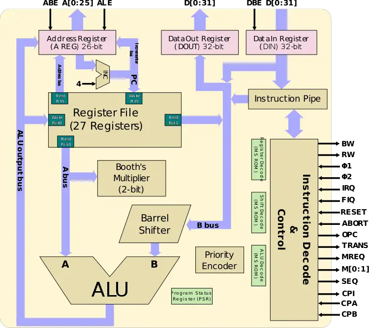
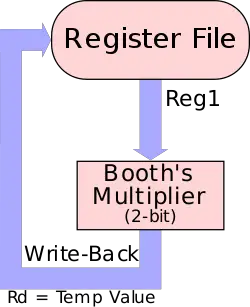
The ARM2 largely builds on the successful ARM1 design, featuring an extremely simple 32-bit single-chip RISC microprocessor implementation with a number of CISC features. The largest change to the pipeline is the augmentation of a new Booth's multiplier that was needed to support the new hardware multiplication instructions.
Pipeline[edit]
The ARM2 utilizes a pipelining technique in order to improve performance and efficiency. At peak performance the ARM2 can reach 10 million instructions per second with an average of 6 MIPS when using a 150 ns row access DRAM. The ARM2's pipeline consists of 3 stages. Previously some instructions may have taken as much as five cycles. With the introduction of hardware multiplication this can now be as high as 16 cycles.
The ARM2 operates on a guaranteed non-overlapping two-phase clock which allowed for level-triggered transfer instead of edge-triggering. The two clock phases are not generated on-die but come from an external oscillator. A complete cycle on the ARM2 is therefore Φ1 + Φ2. To simplify system design, these clocks may be stretched to work in-sync with memory access times.
Fetch[edit]
The Instruction Pipe is a functional block that holds awaiting instructions until execution, it therefore holds a number of instruction sufficient to ensure instructions are always executing at all cycles on all stages.
The program counter on the ARM2 always points to the instruction being fetched. That is, with every instruction being exactly 4 bytes, the currently executing instruction is always PC - 8. During the fetch stage, the address specified by the address register gets sent through the address pins and is fetched from memory.
In conjunction with the address register is a dedicated incrementer which calculates the next address. The actual address for the next instruction will usually come from that incrementer. However, occasionally, the next instruction may also come from the ALU instead. On very rare occasions, the next instruction value can be forced to an exception. When the instruction is coming from the incrementer, the ARM2 will assert this fact on the SEQ pin, allowing the external memory controller to know that the next instruction will in fact be +4 the current instruction, allowing it to determine if an address translation is necessary and prepare ahead. This is done to improve performance because it can make use of Page-Mode DRAM, allowing for more efficient consecutive memory reads.
Decode[edit]
On the second cycle of each instruction, the decode occurs. At this stage the instruction is decoded and the appropriate control signals are generated. The ARM2 implements the decoding in a number of separate units:
- Instruction Decode, performs the top-level decoding
- Register Decode, decodes the register selection field
- ALU Decode, decodes the ALU operation
- Shift Decode, decodes the barrel shifter controls
The Register Decode handles the register selection for both read ports and the write port.
The reason the decode is implemented in a number of separate units is because the ARM2 makes use of microcode ROMs (PLA). Each instruction is decoded into up to four µOP signal-wise. In other words, the ARM instructions are broken down into up to four sets of internal-µOP signals indicating things such as which registers to select or what value to shift by. For some complex operations such as block-transfers, the microsequencer also performs a looping operation for each register.
Execute[edit]
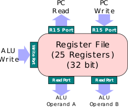
The ARM2 has a physical register file of 27 32-bit registers (same as the architectural register file). This was increased from 25 in the ARM1 for the purpose of processor status. As with the ARM1, Register 15 (R15) is still the Program Counter. 16 of the registers are visible to the user with the reminder only being accessible while in supervisor mode. The register file has two read ports for the operands heading to the ALU and a single write port for the ALU write-back value. Additionally there is a dedicated R15 read and write port.
Each cycle two values are operated on. During clock phase 1 (Φ1) the values are fetched from the appropriate sources into the ALU for execution and during clock phase 2 (Φ2), the 32-bit ALU output is stored onto the Register File write port.
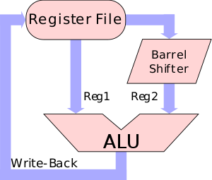
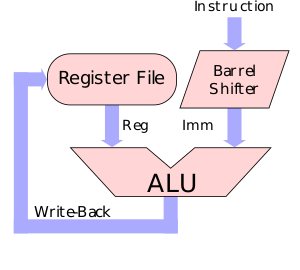
For a typical register-register operation, the first operand is fetched from the register file on Port 0 directly to the ALU while the second operand is fetched from the register file on Port 1 and through the barrel shifter to the ALU. For a register-immediate operation, the first operand is fetched from the register file on Port 0 directly to the ALU while the second operand is fetched from the instruction.
Multiplication[edit]
The ARM1 major performance issue was with multiplication. The ARM1 lacked hardware multiplication which meant software had to resort to a software-based solution (e.g., classic Shift-and-Add Multiplication). For example to perform var = x * 5; one could rewrite it as var = x + (x << 2); to achieve the same result without a multiplication operation. While originally was not thought to be a big problem, software multiplication proved to be a rather serious bottleneck.
This was addressed with the ARM2 which introduced a Booth's Multiplier. Conceptually, the multiplier sits on the "B" operand of the ALU in a similar way to how the barrel shifter sits on the "A" operand of the ALU, however there are some major differences in how they are implemented and operate.
With a number of hard constraints (i.e., die size and power dissipation), the ARM2 solution is a very conservative 2-bit multiplier. Unlike the shifter which can shift the first ALU operand by some amount of bits in almost every instruction, the multiplier is typically inoperative. Only the MUL and MLA make use of it. When that happens the multiplier is invoked. Each cycle the 2-bit Booth's algorithm multiplication is performed. The result is fed through the ALU to a destination register. The destination register is also used to hold the intermediate value which can last up to 16 cycles for all 32 bits. For this reason using the same destination register as the source has been prohibited as it would invoke undefined behavior. Since multiplication is commutative, swapping the two operands around should resolve this problem.
The second instruction implemented, the MLA, supports multiply and accumulate. This instruction takes advantage of the fact that the ALU is situated after the multiplier, allowing a final addition operation to be performed on the result of the multiplication prior to saving the value back into the destination register.
Interrupt[edit]
The ARM2 has fast interrupt capabilities for real-time responses. Exceptions can occur internally or externally to the chip. The average interrupt latency is sub-2 µs with a worst case of sub-6 µs. An interrupt must wait for the currently executing instruction to complete before the interrupt executes. The current instruction completes only when a new instruction starts fetching. When an exception takes place, the processor sets the PC to a specific memory address within the interrupt vector table.
For example, in the case of RESET pin being asserted, the current pipeline gets flushed and the PC is forced to execute from address 0x0.
Multi-Cycle Instruction[edit]
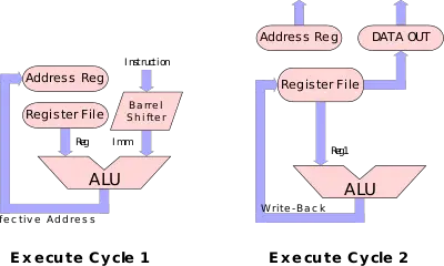
A number of ARM instructions cannot be implemented in a single cycle given the limited resources of the ARM2 (i.e., a single ALU and a single shifter). Instructions such as a store STR (store register) requires calculating the effective address before it can store the data. To solve this problem, the ARM2 effectively runs the same instruction through the execute stage two to three times - in the first execute cycle is used to compute the address while the second execute stage the data store.
For example, in the case of a STR R2, [R3, #4], in the first execute cycle the processor will perform Address = R3 + 4. ARM1 will then run another execute stage for this instruction. In the second cycle, ARM1 will generate a DOUT = R2 at the address generate previously and assert the appropriate pins to indicate this is a write.
ADD | Fetch | Decode | Execute | |||||
|---|---|---|---|---|---|---|---|---|
STR | Fetch | Decode | Address Calculate | Data Store | ||||
ADD | Fetch | Decode | Execute | |||||
ADD | Fetch | Decode | Execute | |||||
ADD | Fetch | Decode | Execute | |||||
| Time | ||||||||
Block-transfer[edit]
- See also: Block-Transfer Instructions
| This section is empty; you can help add the missing info by editing this page. |
Die[edit]
- 2 µm process
- 27,000 transistors
- 5.842 mm x 5.842 mm (230 mils x 230 mils)
- 34.13 mm² die size
All ARM2 Chips[edit]
| List of ARM2-based Processors | ||||||||||||
|---|---|---|---|---|---|---|---|---|---|---|---|---|
| Model | Process | Launched | Frequency | Power Dissipation | Max Memory | |||||||
| VL2333 | ARM2 | 1986 | 8 MHz 0.008 GHz 8,000 kHz | 1 W 1,000 mW 0.00134 hp 0.001 kW | 64 MiB 65,536 KiB 67,108,864 B 0.0625 GiB 6.103516e-5 TiB | |||||||
| VL86C010 | ARM2 | 1987 | 10 MHz 0.01 GHz , 12 MHz10,000 kHz 0.012 GHz 12,000 kHz | 2 W 2,000 mW 0.00268 hp 0.002 kW | 64 MiB 65,536 KiB 67,108,864 B 0.0625 GiB 6.103516e-5 TiB | |||||||
| Count: 2 | ||||||||||||
References[edit]
- Furber, S. B., and A. R. Wilson. "The Acorn RISC Machine ߞ an architectural view." Electronics and Power 33.6 (1987): 402-405.
| codename | ARM2 + |
| core count | 1 + |
| designer | Acorn Computers + |
| first launched | 1986 + |
| full page name | acorn/microarchitectures/arm2 + |
| instance of | microarchitecture + |
| instruction set architecture | ARMv2 + |
| manufacturer | VLSI Technology + and Sanyo + |
| microarchitecture type | CPU + |
| name | ARM2 + |
| pipeline stages | 3 + |
| process | 2,000 nm (2 μm, 0.002 mm) + |
