Semiconductor & Computer Engineering
From WikiChip
File list
This special page shows all uploaded files.
First page |
Previous page |
Next page |
Last page |
| Date | Name | Thumbnail | Size | Description | Versions |
|---|---|---|---|---|---|
| 18:28, 15 July 2017 | snc clusters.png (file) |  |
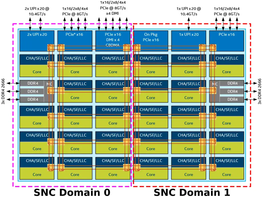
409 KB | Intel {{intel|Skylake|l=arch}} server SNC sub-NUMA clusters. Image by Intel, WikiChip added annotation. | 1 |
| 14:14, 15 July 2017 | skylake sp added cach and vpu.png (file) |  |
78 KB | Intel {{intel|Skylake|l=arch}} SP, core extended with cache and VPU | 1 |
| 10:43, 15 July 2017 | skylake sp buffer windows.png (file) |  |
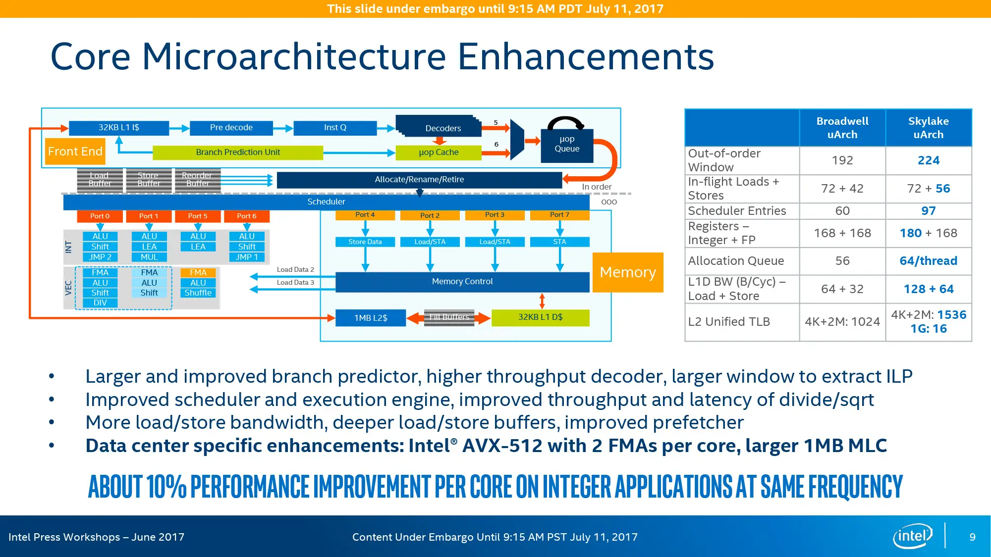
884 KB | Intel {{intel|Skylake|l=arch}} {{intel|SP|l=core}} Buffer Windows by Intel | 1 |
| 21:48, 13 July 2017 | avx-512 flops.png (file) |  |
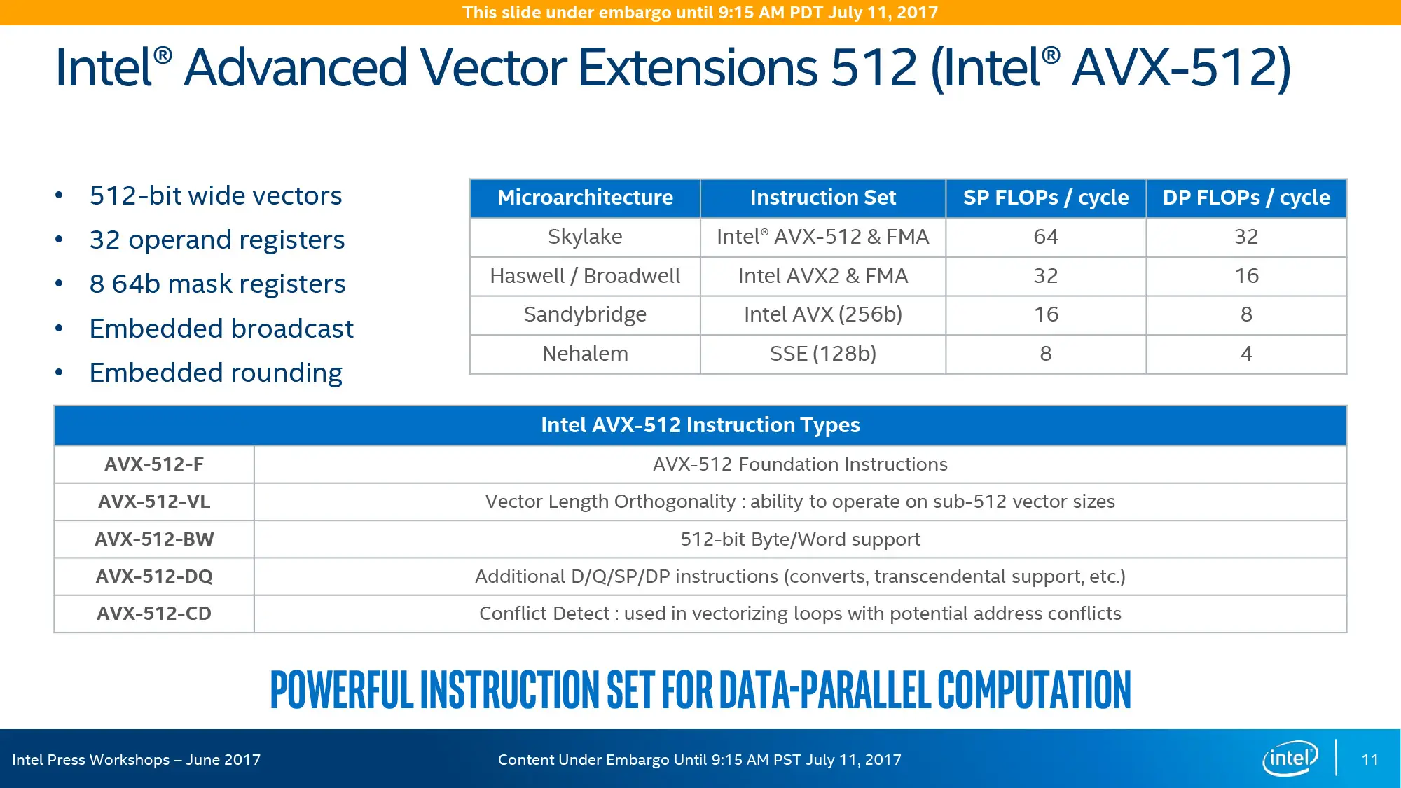
654 KB | Intel {{x86|AVX-512}} FLOPS | 1 |
| 04:39, 13 July 2017 | xeon scalable family decode.png (file) |  |
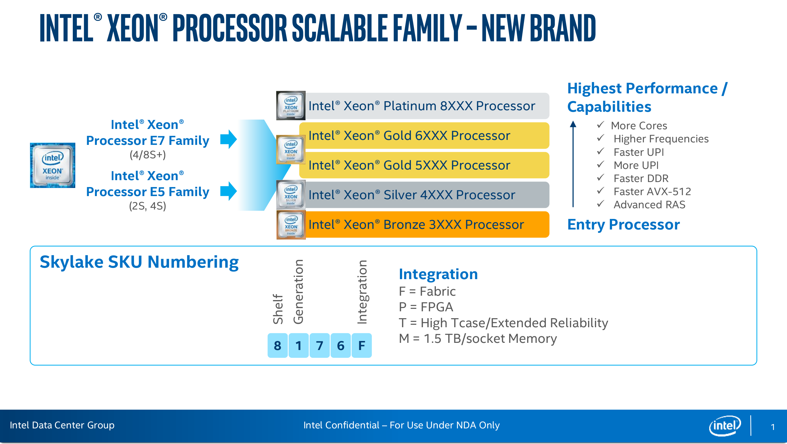
392 KB | {{intel|Skylake SP|l=core}} family decode from previous brands. | 1 |
| 16:54, 11 July 2017 | skylake sp (basic).png (file) | .png) |
1.21 MB | 2 | |
| 22:17, 10 July 2017 | intel 4004 chip.jpg (file) |  |
39 KB | Intel {{intel|4004}}. Image by Intel. | 1 |
| 01:11, 10 July 2017 | Intel Advanced Vector Extensions 2015-2016 Support in GNU Compiler Collection.pdf (file) | 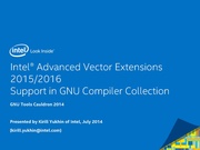 |
1.46 MB | * Intel® {{x86|AVX-512|Advanced Vector Extensions}} 2015/2016 * Support in GNU Compiler Collection * GNU Tools Cauldron 2014 * Presented by Kirill Yukhin of Intel, July 2014 | 1 |
| 00:40, 4 July 2017 | kaby lake u (front; iris).png (file) | .png) |
714 KB | Front of {{intel|Kaby Lake U|l=core}} package by Intel Press. Copyright of Intel. This chip is a Kaby Lake U with Iris Plus GPU and an OPC. | 1 |
| 03:02, 29 June 2017 | acorn computers logo.svg (file) | 128 KB | Acorn Computers logo | 1 | |
| 21:32, 27 June 2017 | two-phase clock.svg (file) |  |
8 KB | My drawing of a two-phase clock diagram. | 1 |
| 21:00, 22 June 2017 | amd x86 memory encryption technology.pdf (file) |  |
1.12 MB | AMD x86 Memory Encryption Technologies David Kaplan, Security Architect, LSS 2016 August 25, 2016 | 1 |
| 20:50, 22 June 2017 | amd sme.png (file) |  |
115 KB | AMD {{amd|Secure Memory Encryption}} (SME) | 1 |
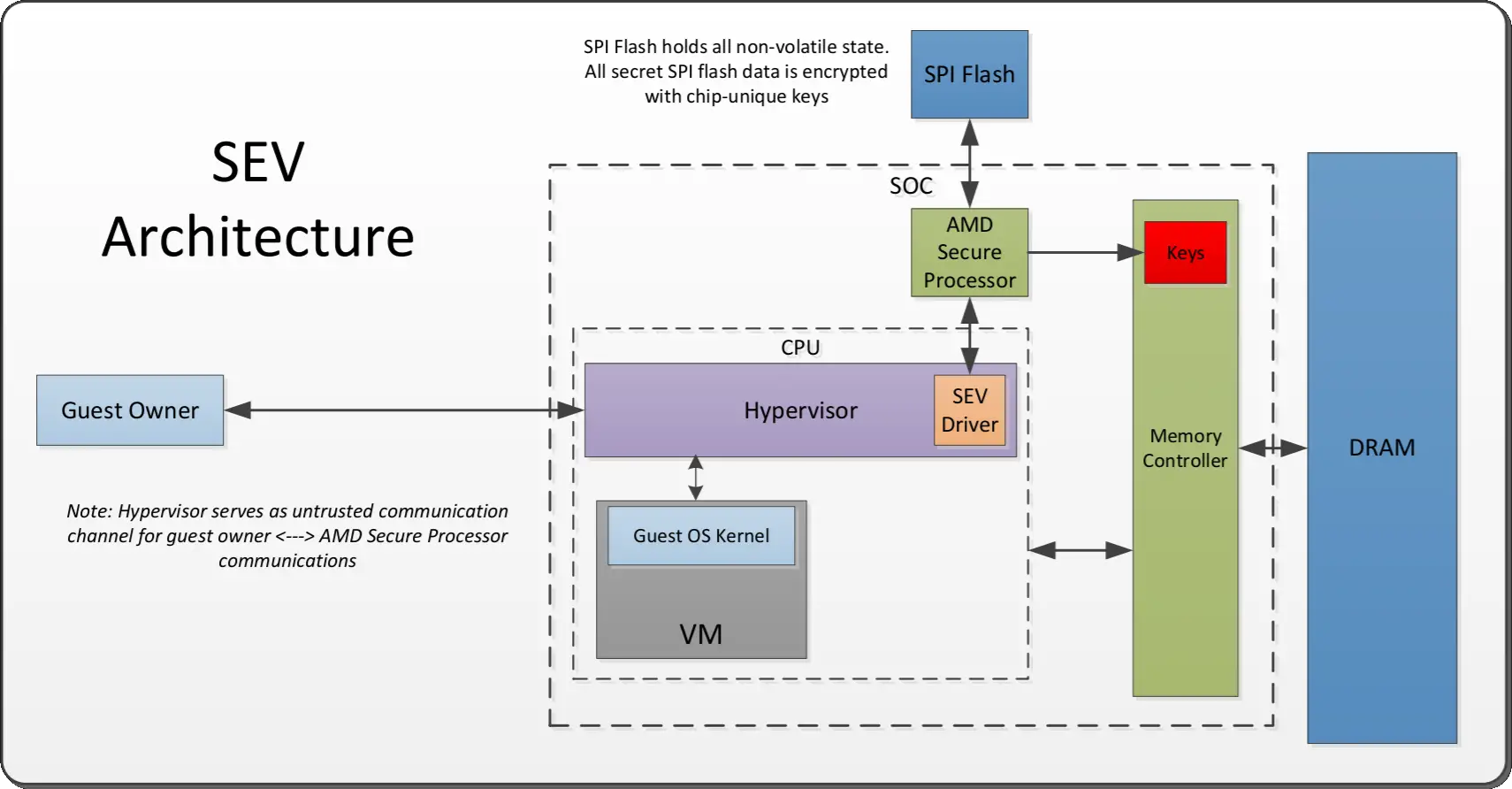
| 20:48, 22 June 2017 | amd sev architecture.png (file) |  |
138 KB | AMD {{amd|Secure Encrypted Virtualization}} (SEV) architecture. | 1 |
| 20:46, 22 June 2017 | amd sev.png (file) |  |
126 KB | AMD's {{amd|Secure Encrypted Virtualization}} (SEV) technology | 1 |
| 18:31, 15 June 2017 | mirc logo.png (file) | 7 KB | mIRC logo. Copyright © mIRC Co. Ltd. | 1 | |
| 00:40, 11 June 2017 | alpha processor inc logo.svg (file) | 1.83 MB | Alpha Processor, Inc (API) logo | 1 | |
| 00:22, 9 June 2017 | alpha 21264 die shot.png (file) |  |
2.71 MB | {{decc|Alpha 21264|l=arch}} die shot by DEC from their own presentation slide that was used at a presentation at MIT, circa. ~1997. Copyright of DEC (now HP?) | 1 |
| 20:04, 29 May 2017 | strongarm die shot.png (file) |  |
1.83 MB | DEC {{decc|StrongARM|l=arch}} die shot by DEC. Copyright DEC, 1996. | 1 |
| 12:49, 29 May 2017 | dec logo.svg (file) | 7 KB | dec logo | 1 | |
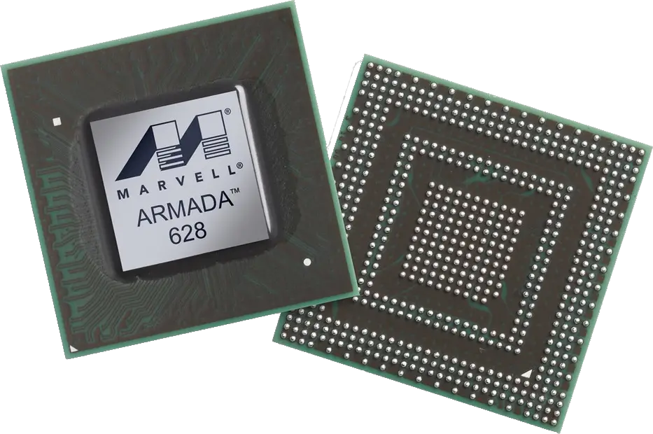
| 15:41, 28 May 2017 | armada 628.png (file) |  |
700 KB | {{marvel|ARMADA}} 628, image by Marvell. | 1 |
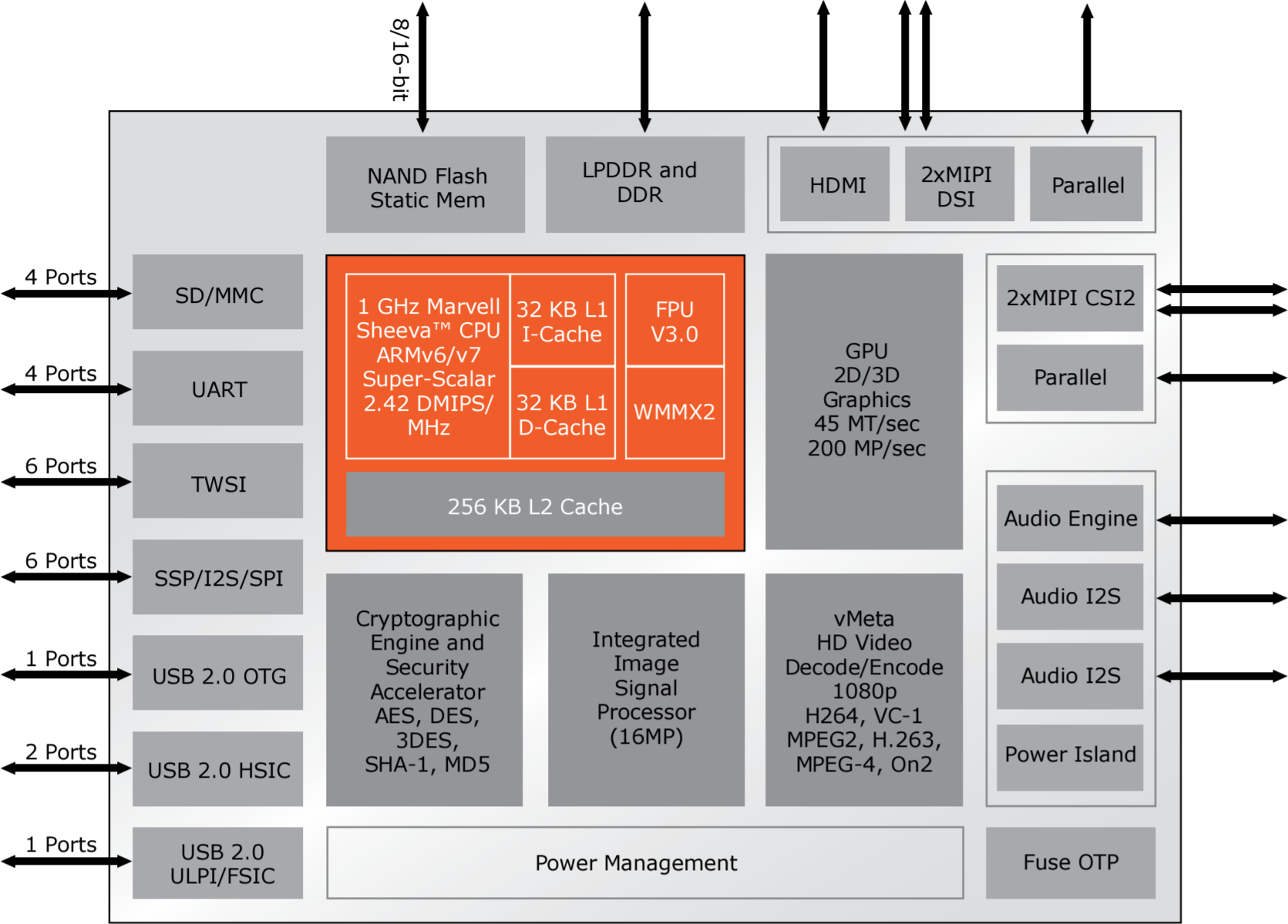
| 14:43, 28 May 2017 | armada 618 block.png (file) |  |
308 KB | {{marvell|ARMADA}} 618 block diagram | 1 |
| 14:39, 28 May 2017 | armada618 pb.pdf (file) | 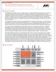 |
404 KB | Marvell {{marvell|ARMADA}} 618 | 1 |
| 13:05, 28 May 2017 | armada610overview.pdf (file) | 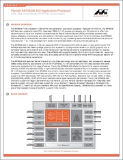 |
263 KB | ARMADA 610 Overview | 1 |
| 13:01, 28 May 2017 | armada610 pb.pdf (file) | 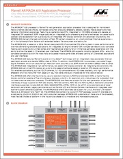 |
407 KB | ARMADA 610 product brief | 1 |
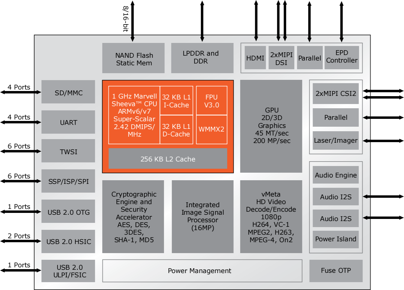
| 12:58, 28 May 2017 | armada 610 block.png (file) |  |
213 KB | {{marvell|ARMADA 600|ARMADA}} 610 block diagram | 1 |
| 08:42, 12 May 2017 | intel 180nm gate.png (file) |  |
410 KB | 2 | |
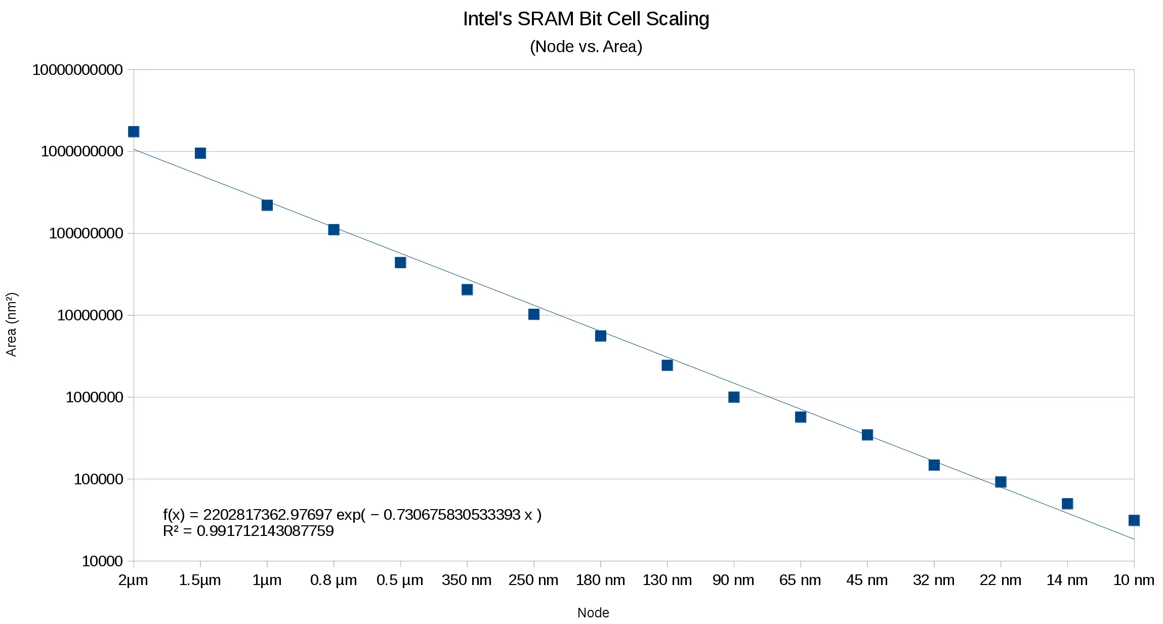
| 08:25, 12 May 2017 | intel sram bit cell scaling.png (file) |  |
82 KB | Intel {{intel|Process}} [[SRAM] bit cell scaling | 1 |
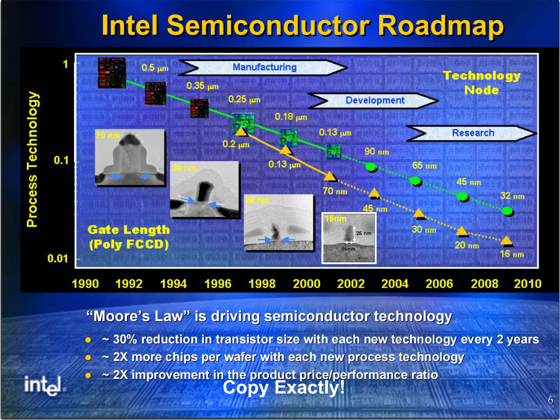
| 05:54, 12 May 2017 | intel historical 2yr process.png (file) |  |
241 KB | Intel {{intel|process}} | 1 |
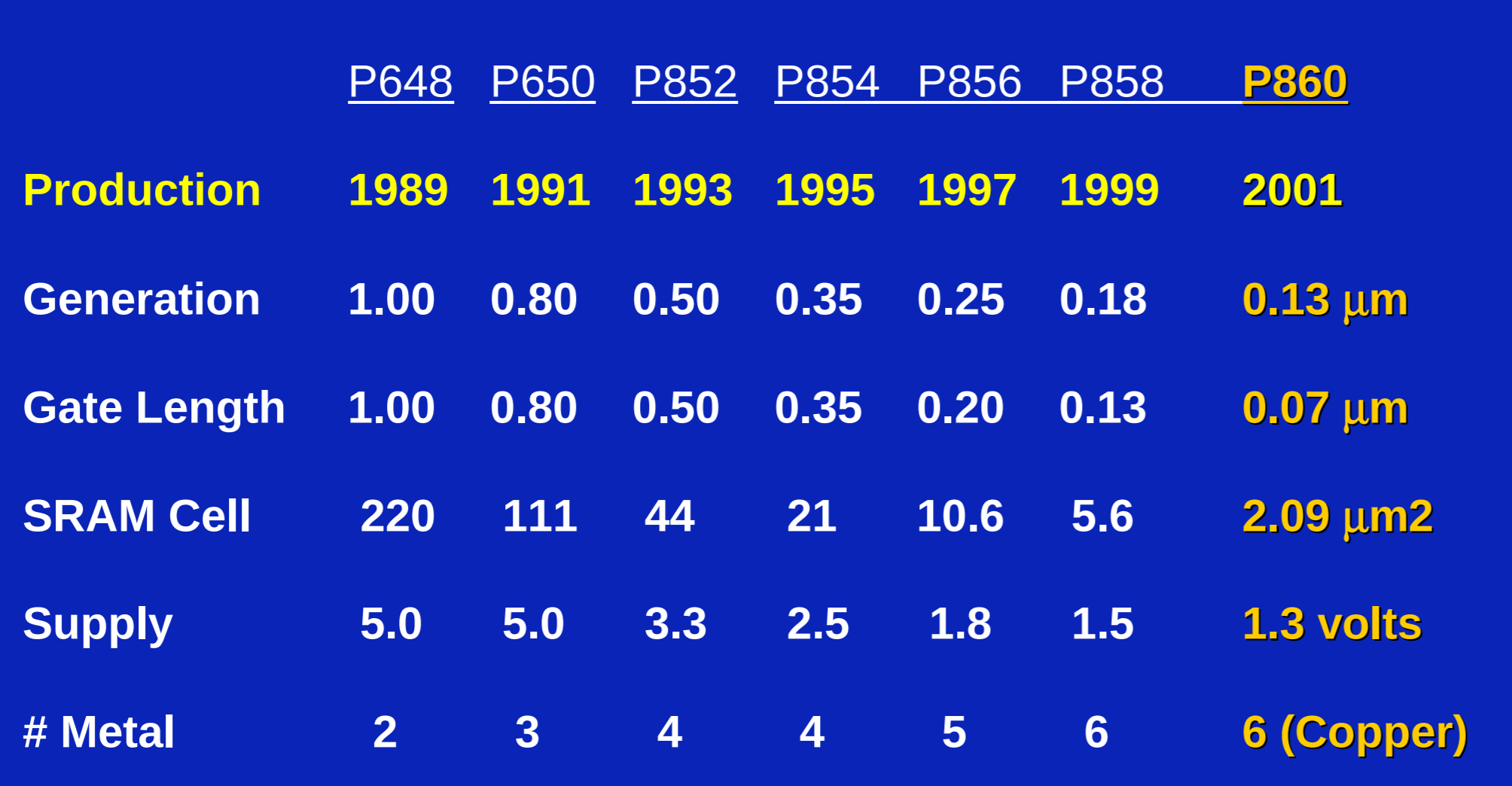
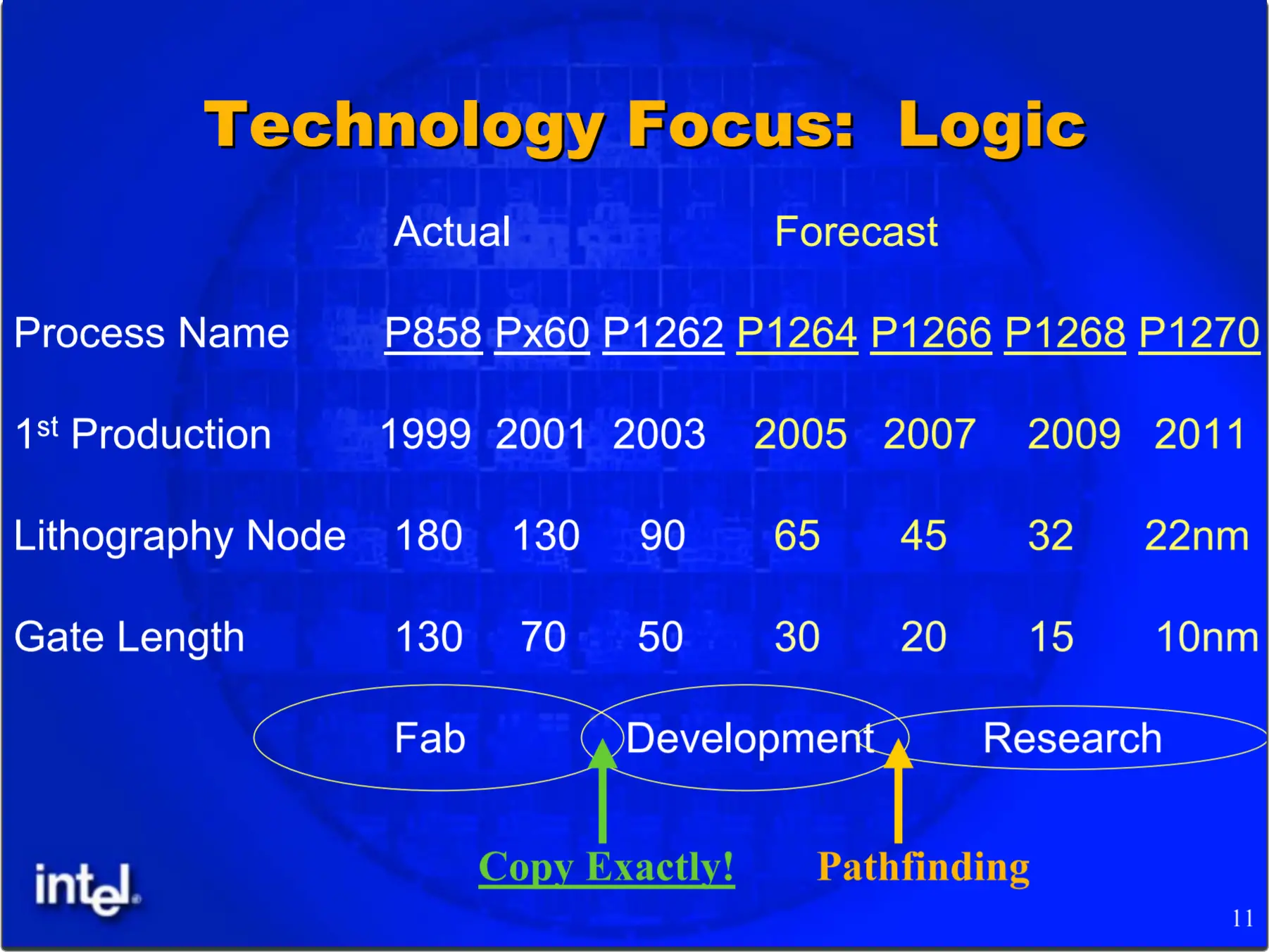
| 14:01, 11 May 2017 | intel roadmap past 180nm.png (file) |  |
2.12 MB | Intel roadmap past 180 nm | 1 |
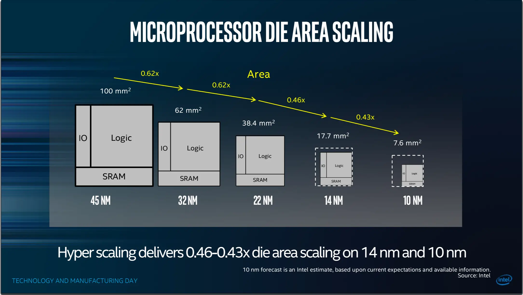
| 13:43, 11 May 2017 | intel scaling from 45nm to 10nm.png (file) |  |
577 KB | Intel scaling from 45 nm to 10 nm | 1 |
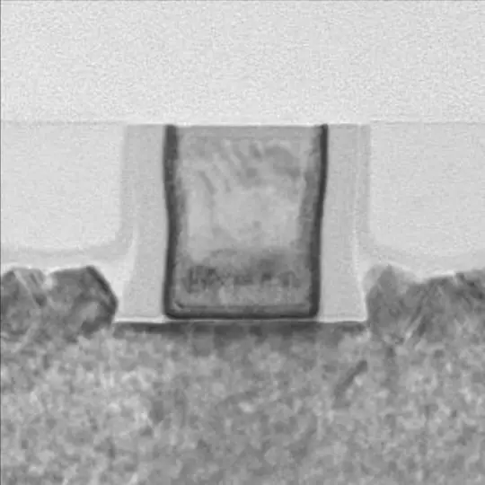
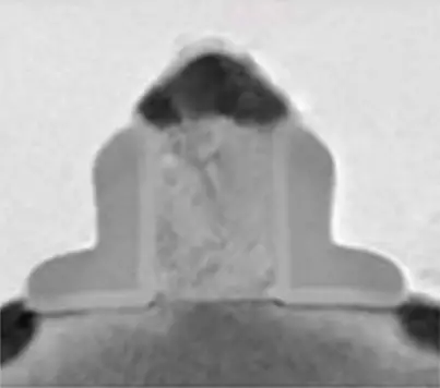
| 13:35, 11 May 2017 | intel 14nm gate top.png (file) |  |
90 KB | Intel 14 nm transistor gate top view | 1 |
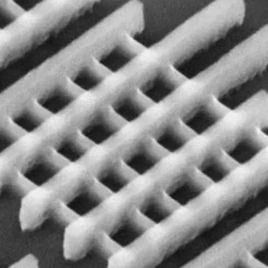
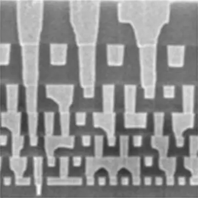
| 13:29, 11 May 2017 | intel 14nm gate interconnect.png (file) |  |
218 KB | Intel 14 nm interconnect | 1 |
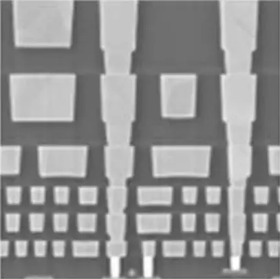
| 13:29, 11 May 2017 | intel 22nm gate interconnect.png (file) |  |
209 KB | Intel 22 nm interconnect | 1 |
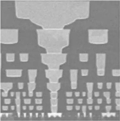
| 13:21, 11 May 2017 | intel 32nm gate interconnect.png (file) |  |
128 KB | Intel 32 nm gate interconnects | 1 |
| 13:21, 11 May 2017 | intel 22nm transistors.png (file) | 157 KB | Intel 22 nm gate | 1 | |
| 13:17, 11 May 2017 | intel 32nm gate.png (file) |  |
162 KB | Intel 32 nm gate | 1 |
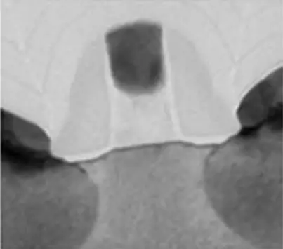
| 13:06, 11 May 2017 | intel 65nm gate.png (file) |  |
50 KB | Intel 65 nm gate | 1 |
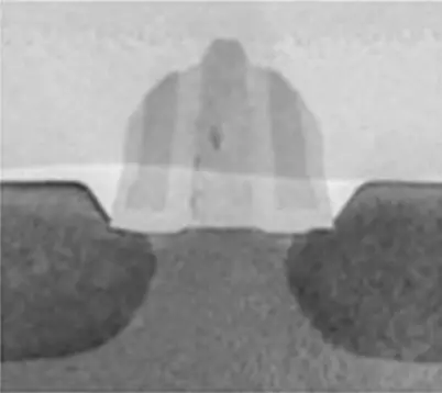
| 13:06, 11 May 2017 | intel 130nm gate.png (file) |  |
48 KB | Intel 130 nm gate | 1 |
| 13:06, 11 May 2017 | intel 90nm gate.png (file) |  |
52 KB | 2 | |
| 13:00, 11 May 2017 | intel 65nm gate interconnect.png (file) |  |
56 KB | Intel 65 nm interconnects | 1 |
| 13:00, 11 May 2017 | intel 90nm gate interconnect.png (file) |  |
79 KB | Intel 90 nm interconnects | 1 |
| 13:00, 11 May 2017 | intel 130nm gate interconnect.png (file) |  |
57 KB | Intel 130 nm interconnects | 1 |
| 12:55, 11 May 2017 | intel 45nm gate interconnects.png (file) |  |
68 KB | Intel 45 nm interconnects | 1 |
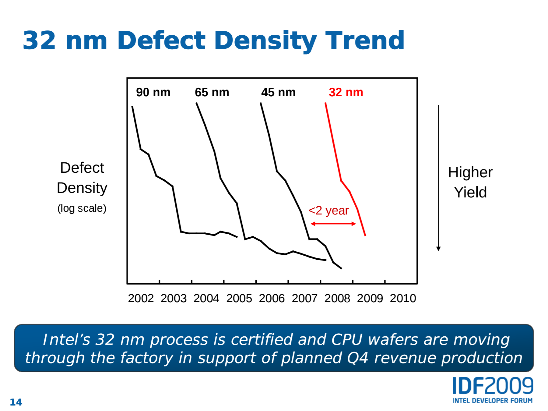
| 12:35, 11 May 2017 | intel 90nm 32nm yield.png (file) |  |
264 KB | Intel 90 nm to 32 nm yield | 1 |
| 06:39, 11 May 2017 | intel fab roadmap from 2003.png (file) |  |
1.03 MB | Intel fab roadmap from 2003. Much of the later nodes changed. | 1 |
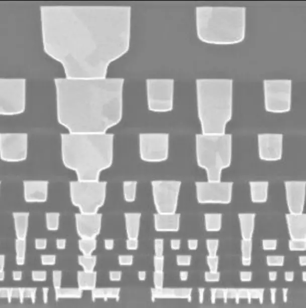
| 06:30, 11 May 2017 | intel sram density scaling.png (file) |  |
703 KB | 2 | |
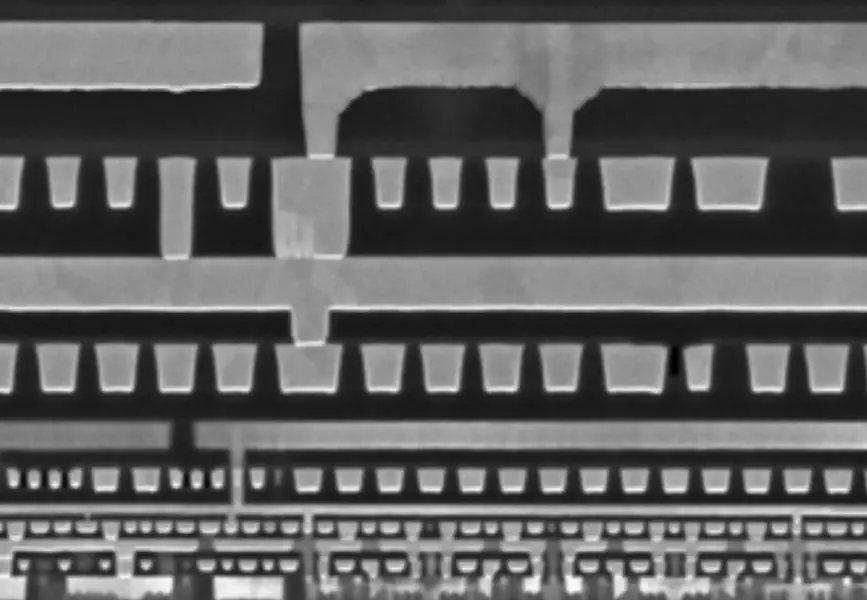
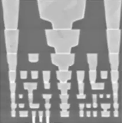
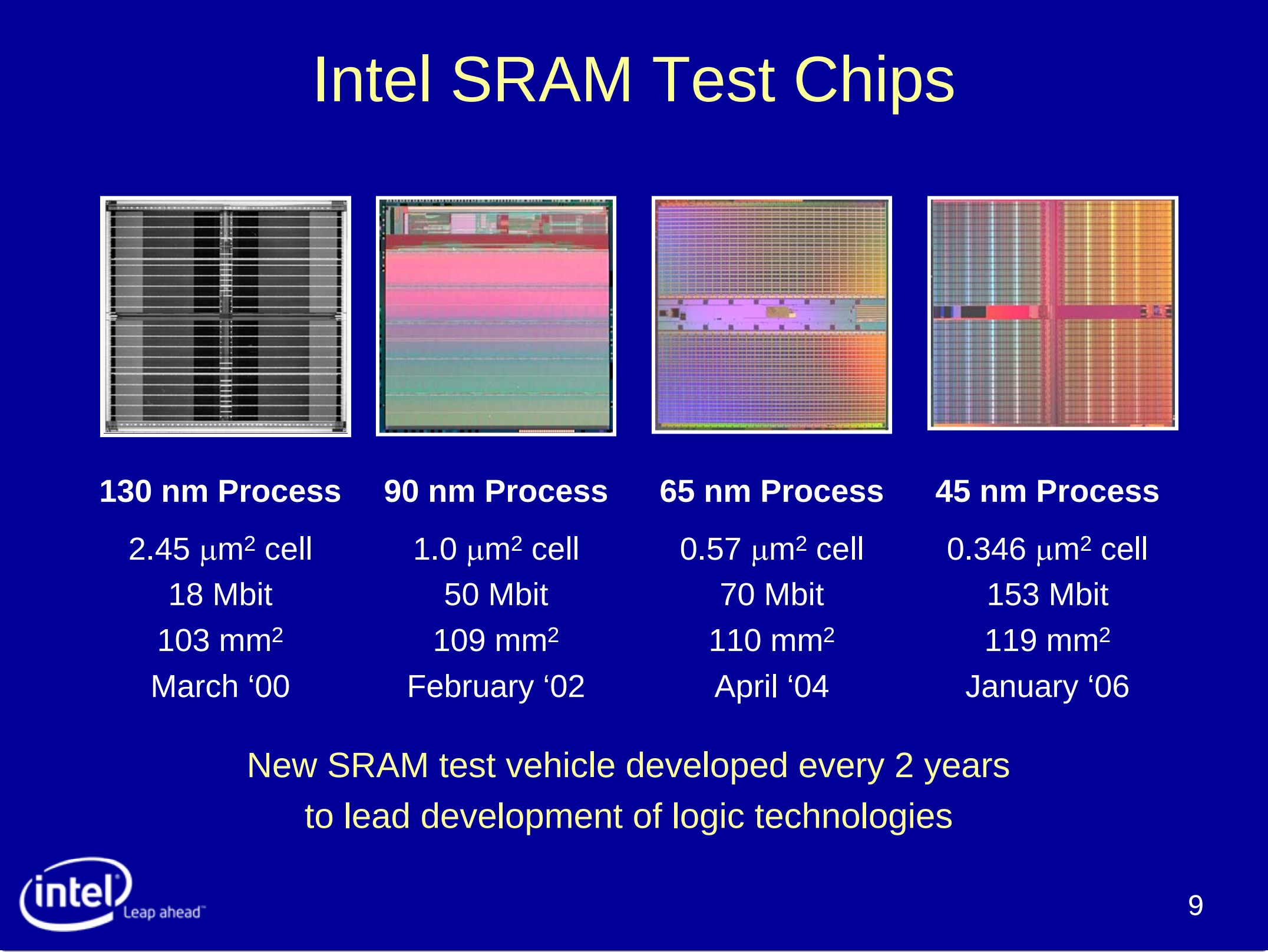
| 03:51, 11 May 2017 | intel sram tests 130nm to 45nm.png (file) |  |
1.06 MB | Intel SRAM test chips from 130 nm to 45 nm | 1 |
| 03:34, 11 May 2017 | intel 1micron yield.png (file) |  |
411 KB | Intel 1 µm yield | 1 |
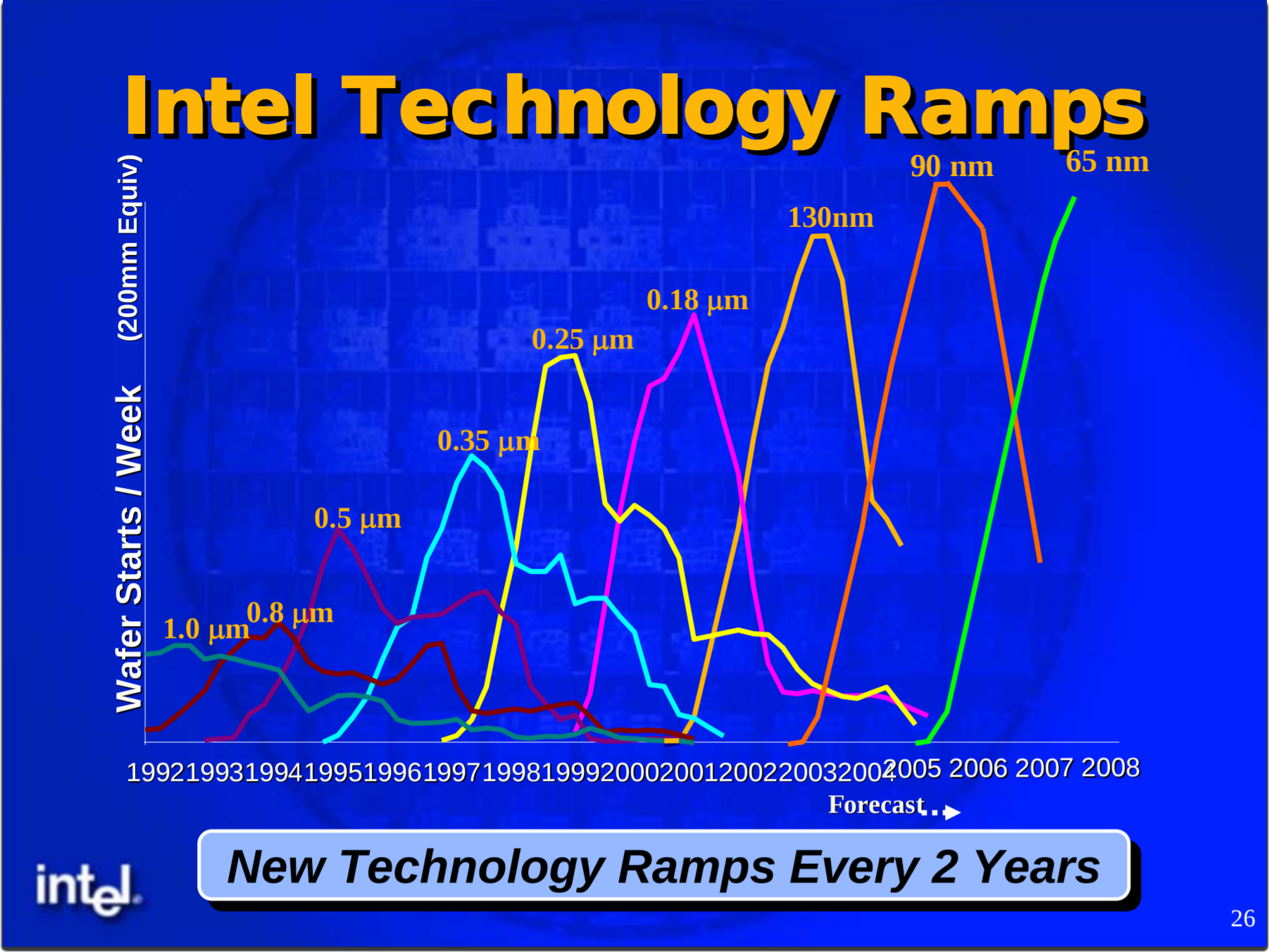
| 03:07, 11 May 2017 | intel tech ramps 1um to 65nm.png (file) |  |
1,010 KB | Intel Tech ramps from 1 µm to 65 nm | 1 |
First page |
Previous page |
Next page |
Last page |