m (→µOP cache & x86 tax) |
(→Pipeline) |
||
| Line 209: | Line 209: | ||
As noted earlier, the µOPs cache has its root in the original {{\\|NetBurst}} trace cache, particularly as far as goals are concerned. But that's where the similarities end. The micro-op cache in Sandy Bridge can be seen as a light-weight, efficient µOPs delivery mechanism that can surpass the legacy pipeline whenever possible. This is different to the trace cache that attempted to effectively replace the entire front-end and use vastly inferior and slow fetch/decode for workloads that the trace cache could not handle. It's worth noting that the trace cache was costly and complicated (having dedicated components such as a trace BTB) and had various side-effects such as needing to flush on context switches. Deficiencies the µOP cache doesn't. Trace caches resulted in a lot of duplication, for example {{\\|NetBurst}}'s 12k uops trace cache had a hit rate comparable to an 8 KiB-16 KiB L1I$ whereas this 1.5K µOPs cache cache is comparable to a 6 KiB instruction cache. This implies a significant storage efficiency of four-fold or greater. | As noted earlier, the µOPs cache has its root in the original {{\\|NetBurst}} trace cache, particularly as far as goals are concerned. But that's where the similarities end. The micro-op cache in Sandy Bridge can be seen as a light-weight, efficient µOPs delivery mechanism that can surpass the legacy pipeline whenever possible. This is different to the trace cache that attempted to effectively replace the entire front-end and use vastly inferior and slow fetch/decode for workloads that the trace cache could not handle. It's worth noting that the trace cache was costly and complicated (having dedicated components such as a trace BTB) and had various side-effects such as needing to flush on context switches. Deficiencies the µOP cache doesn't. Trace caches resulted in a lot of duplication, for example {{\\|NetBurst}}'s 12k uops trace cache had a hit rate comparable to an 8 KiB-16 KiB L1I$ whereas this 1.5K µOPs cache cache is comparable to a 6 KiB instruction cache. This implies a significant storage efficiency of four-fold or greater. | ||
| + | |||
| + | ==== Execution engine ==== | ||
| + | {{empty section}} | ||
== Die == | == Die == | ||
Revision as of 04:15, 30 July 2017
| Edit Values | |
| Sandy Bridge (client) µarch | |
| General Info | |
| Arch Type | CPU |
| Designer | Intel |
| Manufacturer | Intel |
| Introduction | September 13, 2010 |
| Phase-out | November, 2012 |
| Process | 32 nm |
| Core Configs | 2, 4 |
| Pipeline | |
| Type | Superscalar, Superpipeline |
| OoOE | Yes |
| Speculative | Yes |
| Reg Renaming | Yes |
| Stages | 14-19 |
| Decode | 4-way |
| Instructions | |
| ISA | x86-16, x86-32, x86-64 |
| Succession | |
| Contemporary | |
| Sandy Bridge (server) | |
Sandy Bridge (SNB) Client Configuration, formerly Gesher, is Intel's successor to Nehalem, a 32 nm process microarchitecture for mainstream workstations, desktops, and mobile devices. Sandy Bridge is the "Tock" phase as part of Intel's Tick-Tock model which added a significant number of enhancements and features. The microarchitecture was developed by Intel's R&D center in Haifa, Israel.
For desktop and mobile, Sandy Bridge is branded as 2nd Generation Intel Core i3, Core i5, Core i7 processors. For workstations it's branded as first generation Xeon E3.
Contents
Etymology
Sandy Bridge was originally called Gesher which literally means "bridge" in Hebrew. The name was requested to be changed by upper management after a meeting between the development group and analysts brought up that it might be a bad idea to be associated with a failed political party that was eventually dissolved.
The name Sandy Bridge consists of the English translation of "Gesher" with "Sandy" possible referring to the fact that silicon comes from sand.
The Logo on the left was Intel's original ("Gesher") logo for the microarchitecture.
Codenames
| This section is empty; you can help add the missing info by editing this page. |
Process Technology
- Main article: Westmere § Process Technology
Sandy Bridge uses the same 32 nm process used for the Westmere microarchitecture for all mainstream consumer parts.
Architecture
Sandy Bridge's features an entirely new architecture with a brand new core design which is both more performent and more power efficient. Sandy Bridge provides considerable higher integration verses its predecessors.
Key changes from Westmere
- Entirely brand new microarchitecture
- New client ring architecture
- New last level cache architecture
- Multi-bank LLC/Agent architecture
- New System Agent architecture
- Chipset
- Ibex Peak → Cougar Point
- Socket H (LGA-1156) → Socket H2 (LGA-1155)
- Core
- Entirely redesigned
- Front-end
- New µOP cache
- Redesigned branch prediction
- Higher accuracy
- BTB is now a single-level design (from two-level)
- Instruction Queue
- Increased to 20 entries/thread (from 18 entries, shared)
- Improved macro-op fusion (covers almost all jump with most arithmetic now)
- Memory Subsystem
- L1I$ change to 8-way (from 4-way)
- Integrated Graphics
- Integrated graphics is now integrated on the same die (previously was on a second die)
- Dropped QPI controller which linked the two dies
- IMC
- Integrated on-die is now integrated on the same die (previously was on a second die)
- Dropped QPI controller which linked the two dies
| This section requires expansion; you can help adding the missing info. |
Block Diagram
Individual Core
Overview
Sandy Bridge was an entirely new microarchitecture which combines some of the improvements that were implemented in NetBurst along with the original P6 design. In addition to the new core design, Sandy Bridge took full advantage of Intel's 32 nm process which enabled the integration all the components of the chip on a single monolithic die, including the integrated graphics and the integrated memory controller. Sandy Bridge is the first Intel microarchitecture designed as a true system on a chip for high-volume client mainstream market. Previously (e.g., Nehalem) the integrated graphics and the memory interface were fabricated on a separate die which was packaged together and communicated over Intel's QuickPath Interconnect (QPI). The seperate dies were then packaged together as a system on a package.
As stated earlier, the individual cores are an entirely new design which improved both performance and power. Sandy Bridge introduced a number of performance features that brought better-than-linear performance/power as well as a number of enhancements that improved performance while saving power. Intel introduced a number of new vector computation (SIMD) and security instructions which improved floating point performance and throughput as well as speedup the throughput of various encryption algorithms. Sandy Bridge incorporates either two or four physical cores with either four or eight logical cores.
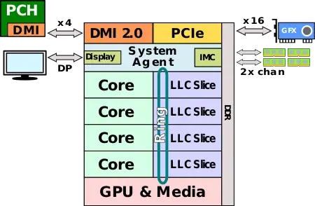
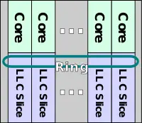
The block diagram on the right is a complete quad-core Sandy Bridge SoC which integrates the new System Agent (SA), the four physical cores along with their companion last level cache (LLC) slices, and the integrated graphics. Interconnecting everything is a complex high-bandwidth low-latency ring on-die which consists of six agents - one for each core and cache slice, one for the system agent, and one for the graphics. The upper portion of the diagram is the System Agent (SA) which incorporates the display controller, the memory controller, and the various I/O interfaces. Previously that component was referred to as the Memory Controller Hub (MCH) when on a separate die. Sandy Bridge incorporates 20 PCIe 2.0 lanes - x4 are used by the DMI with the other x16 lanes designed for a dedicated GPU. The memory controller supports up to dual-channel DDR3-1600 (depending on model).
System Architecture
Sandy Bridge was designed with configurability (i.e. modularity) scalability as the primary system goals. With the full integration of the graphics and memory controller hub on-die Intel needed a new way to efficiently interconnect all the individual components. Modularity was a major design goal for Sandy Bridge. Intel wanted to be able to design the cores and the graphics independently of the rest of the system and be able to detach the graphics and added more cores as desired.
The scalability goal was important for Intel's server configuration where the graphics are dropped and more cores can be added to the ring without compromising performance. Sandy Bridge comprised of a fairly robust ring implementation with bandwidth that can scale to more cores as necessary.
Cache Architecture
As part of the entire system overhaul, the cache architecture has been streamlined and more scalable. Sandy Bridge features a high-bandwidth last level cache which is shared by all the cores as well as the integrated graphics and the system agent. The LLC is an inclusive multi-bank cache architecture that is tightly associative with the individual cores. Each core is paired with a "slice" of LLC which is 2 MiB in size (lower amount for lower-end models). This pairing of cores and cache slices scales with the number of cores which provides a significant performance boost while saving power and bandwidth. Partitioning the data also helps simplifies coherency as well as reduce localized contentions and hot spots.
The last level cache is an inclusive cache with a 64 byte cache line organized as 16-way set associative. Each LLC slice is accessible to all cores. With up to 2 MiB per slice per core, a four-core model will sport a total of 8 MiB. Lower-end/budget models feature a smaller cache slice. This is done by disabling ways of cache in 4-way increments (for a granularity of 512 KiB). The LLC to use latency in Sandy Bridge has been greatly improved from 35-40+ in Nehalem to 26-31 cycles (depending on ring hops).
Cache Box
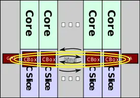
Within each cache slice is cache box. The cache box is the controller and agent serving as the interface between the LLC and the rest of the system (i.e., cores, graphics, and system agent). The cache box implements the ring logic and the address hashing and arbitration. It is also tasked with communicating with the System Agent on cache misses, non-cacheable accesses (such as in the case of I/O pulls), as well as external I/O snoop requests. The cache box is fully pipelined and is capable of working on multiple requests at the same time. Agent requests (e.g., ones from the GPU) are handled by the individual cache boxes via the ring. This is much different to how it was previously done in Westmere where a single unified cache handled everything. The distribution of slices allows Sandy Bridge to have higher associativity bandwidth while reducing traffic.
The entire physical address space is mapped distributively across all the slices using a hash function. On a miss, the core needs decodes the address to figure out which slice ID to request the data from. Physical addresses are hashed at the source in order to prevent hot spots. The cache box is responsible for the maintaining of coherency and ordering between requests. Because the LLC slices are fully inclusive, it can make efficienct use of an on-die snoop filter. Each slice makes use of Core Valid Bits (CVB) which is used to eliminate unnecessary snoops to the cores. A single bit per cache line is needed to indicate if the line may be in the core. Snoops are therefore only needed if the line is in the LLC and a CVB is asserted on that line. This mechanism helps limits external snoops to the cache box most of the time without resorting to going to the cores.
Note that both the cache slices and the cache boxes reside within the same clock domain as the cores themselves - sharing the same voltage and frequency and scaling along with the cores when needed.
Ring Interconnect
In the pursuit of modularity, Sandy Bridge incorporates a new and robust high-bandwidth coherent interconnect that links all the separate components together. The ring is a system of interconnects between the cores, the graphics, the last level cache, and the System Agent. The ring allows Intel to scale up and down efficiently depending on the market segmentation which allows for finer balance of performance, power, and cost. The choice to use a ring makes design and validation easier compared to some of the more complex typologies such as packet routing. It's also easier configurability-wise.
Internally, the ring is composed of four physical independent rings which handle the communication and enforce coherency.
- 32-byte Data ring
- Request ring
- Acknowledge ring
- Snoop ring
The four rings consists of a considerable amount of wiring and routing. Because the routing runs in the upper metal layers over the LLC, the rings have no real impact on die area. As with the LLC slices, the ring is fully pipelined and operates within the core's clock domain as it scales with the frequency of the core. The bandwidth of the ring also scales in bandwidth with each additional core/$slice pair that is added onto the ring, however with more cores the ring becomes more congested and adding latency as the average hop count increases. Intel expected the ring to support a fairly large amount of core before facing real performance issues.
It's important to note that the term ring refers to its structure and not necessarily how the data flows. The ring is not a round-robin and requests may travel up or down as needed. The use of address hashing allows the source agent to know exactly where the destination is. In order reduce latency, the ring is designed such as that all accesses on the ring always picks the shortest path. Because of this aspect of the ring and the fact that some requests can take longer than others to complete, the ring might have requests being handled out of order. It is the responsibility of the source agents to handle the ordering requirements. The ring cache coherency protocol is largely an enhancement based on Intel's QPI protocols with MESI-based source snooping protocol. On each cycle, the agents receive an indication whether there is an available slot on the ring for communication in the next cycle. When asserted, the agent can sent any type of communication (e.g. data or snoop) on the ring the following cycle.
The data ring is 32 bytes meaning each slice can pass half a cache line to the ring each cycle. This means that a dual-core operating at 4 GHz on both cores will have a bandwidth of 256 GB/s.
System Agent
- Main article: Intel's System Agent
The System Agent (SA) is a centralized peripheral device integration unit. It contains what was previously the traditional Memory Controller Hub (MCH) which includes all the I/O such as the PCIe, DMI, and others. Additionally the SA incorporates the memory controller and the display engine which works in tandem with the integrated graphics. The major enabler for the new System Agent is in fact the 32 nm process which allowed for considerably higher integration, over a dozen clock domains and PHYs.
The system agent interfaces with the rest of the system via the ring in a similar manner to the cache boxes in the LLC slices. It is also in charge of handling I/O to cache coherency. The SA enables direct memory access (DMA) allows devices to snoop the cache hierarchy. Address conflicts resulting from multiple concurrent requests associated with the same cache line are also handled by the SA.
With Sandy Bridge, Intel introduced a large number of power features to save powers depending on the workload, temperature, and what's I/O is being utilized. The various power features are handled at the system agent as well.
Core
Sandy Bridge can be considered the first brand new microarchitecture since the introduction of NetBurst and P6 prior. Sandy Bridge went back to the drawing board and incorporated many of beneficial elements from P6 as well as NetBurst. While NetBurst ended up being a seriously flawed architecture, its design was driven by a number of key innovations which were re-implemented and enhanced in Sandy Bridge. This is different from earlier architectures (i.e., Core through Nehalem) which were almost exclusively enhancements of P6 with nothing inherited from P4. Every aspect of the core was improved over its predecessors with very functional block being improved.
Pipeline
The Sandy Lake core focuses on extracting performance and reducing power through a great number ways. Intel placed heavy emphasis in the cores on performance enhancing features that can provide more-than-linear performance-to-power ratio as well as features that provide more performance while reducing power. The various enhancements can be found in both the front-end and the back-end of the core.
Broad Overview
| This section is empty; you can help add the missing info by editing this page. |
Front-end
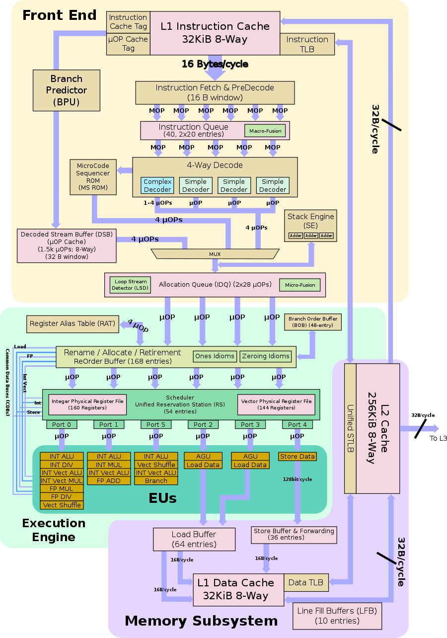
The front-end is is tasked with the challenge of fetching the complex x86 instructions from memory, decoding them, and delivering them to the execution units. In other words, the front end needs to be able to consistently deliver enough µOPs from the instruction code stream to keep the back-end busy. When the back-end is not being fully utilized, the core is not reaching its full performance. A weak or under-performing front-end will directly affect the back-end, resulting in a poorly performing core. In the case of Sandy Bridge base, this challenge is further complicated by various redirection such as branches and the complex nature of the x86 instructions themselves.
The entire front-end was redesigned from the ground up in Sandy Bridge. The four major changes in the front-end of Sandy Bridge is the entirely new µOP cache, the overhauled branch predictor and further decoupling of the front-end, and the improved macro-op fusion capabilities. All those features not only improve performance but they also reduce power at the same time.
Fetch & pre-decoding
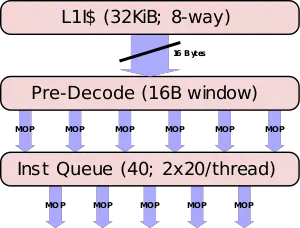
Blocks of memory arrive at the core from either the cache slice or further down the ring from one of the other cache slice. On occasion, far less desirably, from main memory. On their first pass, instructions should have already been prefetched from the L2 cache and into the L1 cache. The L1 is a 32 KiB, 64B line, 8-way set associative cache. The instruction cache is identical in size to that of Nehalem's but its associativity was increased to 8-way. Sandy Bridge fetching is done on a 16-byte fetch window. A window size that has not changed in a number of generations. Up to 16 bytes of code can be fetched each cycle. Note that fetcher is shared evenly between two thread, so that each thread gets every other cycle. At this point they are still macro-ops (i.e. variable-length x86 architectural instruction). Instructions are brought into the pre-decode buffer for initial preparation.
x86 instructions are complex, variable length, have inconsistent encoding, and may contain multiple operations. At the pre-decode buffer the instructions boundaries get detected and marked. This is a fairly difficult task because each instruction can vary from a single byte all the way up to fifteen. Moreover, determining the length requires inspecting a couple of bytes of the instruction. In addition boundary marking, prefixes are also decoded and checked for various properties such as branches. As with previous microarchitectures, the pre-decoder has a throughput of 6 macro-ops per cycle or until all 16 bytes are consumed, whichever happens first. Note that the predecoder will not load a new 16-byte block until the previous block has been fully exhausted. For example, suppose a new chunk was loaded, resulting in 7 instructions. In the first cycle, 6 instructions will be processed and a whole second cycle will be wasted for that last instruction. This will produce the much lower throughput of 3.5 instructions per cycle which is considerably less than optimal. Likewise, if the 16-byte block resulted in just 4 instructions with 1 byte of the 5th instruction received, the first 4 instructions will be processed in the first cycle and a second cycle will be required for the last instruction. This will produce an average throughput of 2.5 instructions per cycle. Note that there is a special case for length-changing prefix (LCPs) which will incur additional pre-decoding costs. Real code is often less than 4 bytes which usually results in a good rate.
Branch Predictor
The fetch works along with the branch prediction unit (BPU) which attempts to guess the flow of instructions. All branches utilize the BPU for their predictions, including returns, indirect calls and jumps, direct calls and jumps, and conditional branches. As with almost every iteration of Intel's microarchitecture, the branch predictor has also been improved. An improvement to the branch predictor has the unique consequence of directly improving both performance and power efficiency. Due to the deep pipeline, a flush is a rather expensive event which ends up discarding over 150 instructions that are in-flight. One of the big changes that was done in Nehalem and was carried over into Sandy Bridge is the further decoupling of the BPU between the front-end and the back-end. Prior to Nehalem, the entire pipeline had to be fully flushed before the front-end could resume operations. This was redone in Nehalem and the front-end can start decoding right away as soon as the correct path become known - all while the back-end is still flushing the badly speculated µOPs. This results in a reduced penalty (i.e. lower latency) for wrong target prediction. In addition, a large portion of the branch predictor in Sandy Bridge was actually entirely redesigned. The branch predictor incorporates the same mechanisms found in Nehalem: Indirect Target Array (ITA), the branch target buffer (BTB), Loop Detector (LD), and the renamed return stack buffer (RSB).
For near returns, Sandy Bridge has the same 16-entry return stack buffer. The BTB in Sandy Bridge is a single level structure that holds twice as many entries as Nehalem's L1/2 BTBs. This change should result increase the prediciton coverage. It's interesting to note that prior to Nehalem, Intel previously used a single-level design in Core. This is done through compactness. Since most branches do not need nearly as many bits per branch, for larger displacements, a separate table is used. Sandy Bridge appears to have a BTB table with 4096 targets, same as NetBurst, which is organized as 1024 sets of 4 ways.
The global branch history table was not increased with Sandy Bridge, but was enhanced by removing certain branches from history that did not improve predictions.
Instruction Queue & MOP-Fusion
| MOP-Fusion Example: | ||
cmp eax, [mem] jne loop |
→ | cmpjne eax, [mem], loop |
- See also: Macro-Operation Fusion
The pre-decoded instructions are delivered to the Instruction Queue (IQ). In Nehalem, the Instruction Queue has been increased to 18 entries which were shared by both threads. Sandy Bridge increased that number to 20 but duplicated over for each thread (i.e. 40 total entries).
One key optimization the instruction queue does is macro-op fusion. Sandy Bridge can fuse two macro-ops into a single complex one in a number of cases. In cases where a test or compare instruction with a subsequent conditional jump is detected, it will be converted into a single compare-and-branch instruction. With Sandy Bridge, Intel expanded the macro-op fusion capabilities further. Macro-fusion can now work with just about jump instruction such as ADD and SUB. This means that more new cases are now fusable. Perhaps the most important case is in most typical loops which have a counter followed by an exist condition. Those should now be fused. Those fused instructions remain fused throughout the entire pipeline and get executed as a single operation by the branch unit thereby saving bandwidth everywhere. Only one such fusion can be performed each cycle.
Decoding
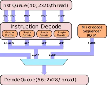
Up to four instructions (or five in cases where one of the instructions was macro-fused) pre-decoded instructions are sent to the decoders each cycle. Like the fetchers, the Decoders alternate between the two thread each cycle. Decoders read in macro-operations and emit regular, fixed length µOPs. The decoders organization in Sandy Bridge has been kept more or less the same as Nehalem. As with its predecessor, Sandy Bridge features four decodes. The decoders are asymmetric; the first one, Decoder 0, is a complex decoder while the other three are simple decoders. A simple decoder is capable of translating instructions that emit a single fused-µOP. By contrast, a complex decoder can decode anywhere from one to four fused-µOPs. Overall up to 4 simple instructions can be decoded each cycle with lesser amounts if the complex decoder needs to emit addition µOPs; i.e., for each additional µOP the complex decoder needs to emit, 1 less simple decoder can operate. In other words, for each additional µOP the complex decoder emits, one less decoder is active.
Sandy Bridge brought about the first 256-bit SIMD set of instructions called AVX. This extension expanded the sixteen pre-existing 128-bit XMM registers to 256-bit YMM registers for floating point vector operations (note that Haswell expanded this further to Integer operations as well). Most of the new AVX instructions have been designed as simple instructions that can be decoded by the simple decoders
MSROM & Stack Engine
There are more complex instructions that are not trivial to be decoded even by complex decoder. For instructions that transform into more than four µOPs, the instruction detours through the microcode sequencer (MS) ROM. When that happens, up to 4 µOPs/cycle are emitted until the microcode sequencer is done. During that time, the decoders are disabled.
x86 has dedicated stack machine operations. Instructions such as PUSH, POP, as well as CALL, and RET all operate on the stack pointer (ESP). Without any specialized hardware, such operations would would need to be sent to the back-end for execution using the general purpose ALUs, using up some of the bandwidth and utilizing scheduler and execution units resources. Since Pentium M, Intel has been making use of a Stack Engine. The Stack Engine has a set of three dedicated adders it uses to perform and eliminate the stack-updating µOPs (i.e. capable of handling three additions per cycle). Instruction such as PUSH are translated into a store and a subtraction of 4 from ESP. The subtraction in this case will be done by the Stack Engine. The Stack Engine sits after the decoders and monitors the µOPs stream as it passes by. Incoming stack-modifying operations are caught by the Stack Engine. This operation alleviate the burden of the pipeline from stack pointer-modifying µOPs. In other words, it's cheaper and faster to calculate stack pointer targets at the Stack Engine than it is to send those operations down the pipeline to be done by the execution units (i.e., general purpose ALUs).
µOP cache & x86 tax
Decoding the variable-length, inconsistent, and complex x86 instructions is a nontrivial task. It's also expensive in terms of performance and power. Therefore, the best way for the pipeline to avoid those things is to simply not decode the instructions. This is exactly what Intel has done with Sandy Bridge and what's perhaps the single biggest feature that has been added to the core. With Sandy Bridge Intel introduced a new µOP cache unit or perhaps more appropriately called the Decoded Stream Buffer (DSB). The µOP cache is a unique unit which not only can substantially improve performance but it does so while significantly reduce power.
On the surface, the µOP cache can be conceptualized as a second instruction cache unit that is subset of the level one instruction cache. What's unique about it is that it stores actual decoded instructions (i.e., µOPs). While it shares many of the goals of NetBurst's trace cache, the two implementations are entirely different. The idea behind both mechanisms is to increase the front-end bandwidth by reducing reliance on the decoders.
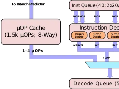
At any given time, the core operates on chunks of 32 bytes of the instruction stream. The µOP cache operates on full 32 B windows as well. This is by design so that the µOP cache could store and evict entire windows. Intel refers to the traditional pipeline path as the "legacy decode pipeline". On initial iteration, all instructions go through the legacy decode pipeline. Once the entire stream window is decoded and makes it to the allocation queue, a copy of the window is inserted into the µOP cache. This occurs simultaneously with all other operations; i.e., no additional cycles or stages are added for this functionality. On all subsequent iterations, the cached pre-decoded stream is sent directly to the allocation queue - bypassing fetching, predecoding, and decoding, saving power and increasing throughput.
The micro-op cache is organized into 32 sets of 8 cache lines with each line holding up to 6 µOP for a total of 1,536 µOPs. The cache is competitively shared between the two threads and can also hold pointers to the microcode sequencer rom. It's also virtually addressed and is a strict subset of the L1 instruction cache (that is, the L1 is inclusive of the µOP cache). Each line includes additional meta info for the number of contained µOP and their length.
Note that a single stream window of 32 bytes can only span 3 ways. With 6 µOP for a total, this means a maximum of 18 µOPs per window can be cached by the µOP cache. This consequently means a 32 byte window that generates more than 18 µOPs will not be allocated in the µOP cache and will have to go through the legacy decode pipeline instead.
The µOP cache has an average hit rate of around 80%. During the instruction fetch, the branch predictor will probe the µOPs cache tags. A hit in the µOP allows for up to 4 µOPs per cycle to be sent directly to the Instruction Decode Queue (IDQ), bypassing all the pre-decoding and decoding that would otherwise have to be done. During those cycles, the rest of the front-end is entirely clock-gated which is how the substantial power saving is gained. Whereas the legacy decode path works in 16-byte instruction fetch windows, the µOP cache has no such restriction and can deliver 4 µOPs/cycle corresponding to the much bigger 32-byte window. Since a single window can be made of up to 18 µOPs, up to 5 whole cycles may be required to read out the entire decoded stream. Nonetheless, the µOPs cache can deliver consistently higher bandwidth than the legacy pipeline.
It's interesting to note that the µOPs cache only operates on full window, that is, a full 32B window that has all the µOPs cached. Any partial hits are required to go through the legacy decode pipeline. The choice to not handle partial cache is rooted in the µOPs' efficiency. On partial window hits you'd end up emitting some µOPs from the micro-op cache as well has having the legacy decode pipeline decoding the remaining missed µOPs. Effectively multiple components will end up emitting µOPs. Not only such mechanism would increase complexity, but it's also unclear how much, if any, benefits would be gained by that.
As noted earlier, the µOPs cache has its root in the original NetBurst trace cache, particularly as far as goals are concerned. But that's where the similarities end. The micro-op cache in Sandy Bridge can be seen as a light-weight, efficient µOPs delivery mechanism that can surpass the legacy pipeline whenever possible. This is different to the trace cache that attempted to effectively replace the entire front-end and use vastly inferior and slow fetch/decode for workloads that the trace cache could not handle. It's worth noting that the trace cache was costly and complicated (having dedicated components such as a trace BTB) and had various side-effects such as needing to flush on context switches. Deficiencies the µOP cache doesn't. Trace caches resulted in a lot of duplication, for example NetBurst's 12k uops trace cache had a hit rate comparable to an 8 KiB-16 KiB L1I$ whereas this 1.5K µOPs cache cache is comparable to a 6 KiB instruction cache. This implies a significant storage efficiency of four-fold or greater.
Execution engine
| This section is empty; you can help add the missing info by editing this page. |
Die
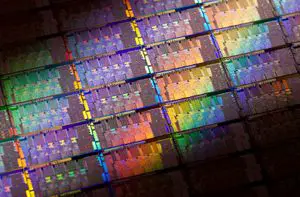
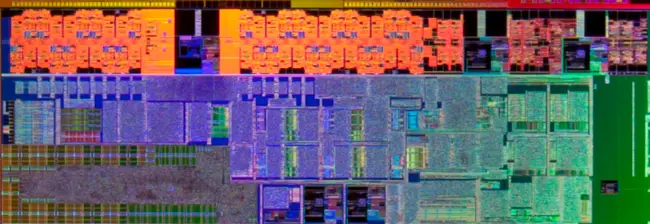
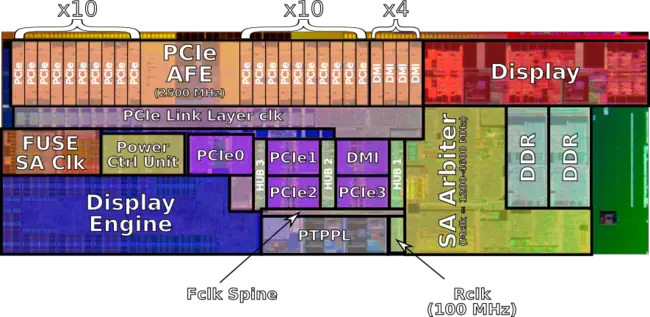
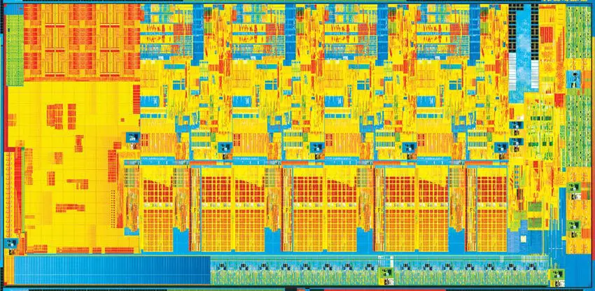
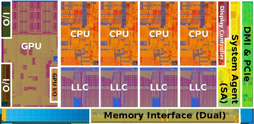
Sandy Bridge desktop and mobile consist of 2 and 4 core models, each with their own die. One of the most noticeable changes on die is the integration of the GPU and the memory interface. The major components of the die are:
- System Agent
- CPU Core
- Ring bus interconnect
- Memory Controller
System Agent
The System Agent (SA) contains the Display Engine (DE), Power management units, and the various I/O buses.
Quad-Core
Quad-core Sandy Bridge die:
- 995,000,000 transistors
- 32 nm process
- 216 mm² die size
- 4 CPU cores
- 1 GPU core
- 12 EUs
Cores
| This section is empty; you can help add the missing info by editing this page. |
All Sandy Bridge Chips
... further results| Sandy Bridge Chips | |||||||||||
|---|---|---|---|---|---|---|---|---|---|---|---|
| Main processor | IGP | ||||||||||
| Model | µarch | Platform | Core | Launched | SDP | TDP | Freq | Max Mem | Name | Freq | Max Freq |
| 787 | Sandy Bridge | Sandy Bridge M | Sandy Bridge M | July 2011 | 17 W 17,000 mW 0.0228 hp 0.017 kW | 1,300 MHz 1.3 GHz 1,300,000 kHz | 16,384 MiB 16,777,216 KiB 17,179,869,184 B 16 GiB 0.0156 TiB | HD Graphics (Sandy Bridge) | 350 MHz 0.35 GHz 350,000 KHz | 950 MHz 0.95 GHz 950,000 KHz | |
| 797 | Sandy Bridge | Sandy Bridge M | Sandy Bridge M | January 2012 | 17 W 17,000 mW 0.0228 hp 0.017 kW | 1,400 MHz 1.4 GHz 1,400,000 kHz | 16,384 MiB 16,777,216 KiB 17,179,869,184 B 16 GiB 0.0156 TiB | HD Graphics (Sandy Bridge) | 350 MHz 0.35 GHz 350,000 KHz | 950 MHz 0.95 GHz 950,000 KHz | |
| 807 | Sandy Bridge | Sandy Bridge M | Sandy Bridge M | July 2012 | 17 W 17,000 mW 0.0228 hp 0.017 kW | 1,500 MHz 1.5 GHz 1,500,000 kHz | 16,384 MiB 16,777,216 KiB 17,179,869,184 B 16 GiB 0.0156 TiB | HD Graphics (Sandy Bridge) | 350 MHz 0.35 GHz 350,000 KHz | 950 MHz 0.95 GHz 950,000 KHz | |
| 807UE | Sandy Bridge | Sandy Bridge M | Sandy Bridge M | July 2012 | 10 W 10,000 mW 0.0134 hp 0.01 kW | 1,000 MHz 1 GHz 1,000,000 kHz | 4,096 MiB 4,194,304 KiB 4,294,967,296 B 4 GiB 0.00391 TiB | HD Graphics (Sandy Bridge) | 350 MHz 0.35 GHz 350,000 KHz | 800 MHz 0.8 GHz 800,000 KHz | |
| 817 | Sandy Bridge | Sandy Bridge M | Sandy Bridge M | 2012 | 17 W 17,000 mW 0.0228 hp 0.017 kW | 1,600 MHz 1.6 GHz 1,600,000 kHz | 16,384 MiB 16,777,216 KiB 17,179,869,184 B 16 GiB 0.0156 TiB | HD Graphics (Sandy Bridge) | 350 MHz 0.35 GHz 350,000 KHz | 800 MHz 0.8 GHz 800,000 KHz | |
| 827 | Sandy Bridge | Sandy Bridge M | Sandy Bridge M | 2012 | 17 W 17,000 mW 0.0228 hp 0.017 kW | 1,400 MHz 1.4 GHz 1,400,000 kHz | 16,384 MiB 16,777,216 KiB 17,179,869,184 B 16 GiB 0.0156 TiB | HD Graphics (Sandy Bridge) | 350 MHz 0.35 GHz 350,000 KHz | 800 MHz 0.8 GHz 800,000 KHz | |
| 827E | Sandy Bridge | Sandy Bridge M | Sandy Bridge M | July 2011 | 17 W 17,000 mW 0.0228 hp 0.017 kW | 1,400 MHz 1.4 GHz 1,400,000 kHz | 16,384 MiB 16,777,216 KiB 17,179,869,184 B 16 GiB 0.0156 TiB | HD Graphics (Sandy Bridge) | 350 MHz 0.35 GHz 350,000 KHz | 800 MHz 0.8 GHz 800,000 KHz | |
| 837 | Sandy Bridge | Sandy Bridge M | Sandy Bridge M | 2012 | 17 W 17,000 mW 0.0228 hp 0.017 kW | 1,800 MHz 1.8 GHz 1,800,000 kHz | 16,384 MiB 16,777,216 KiB 17,179,869,184 B 16 GiB 0.0156 TiB | HD Graphics (Sandy Bridge) | 350 MHz 0.35 GHz 350,000 KHz | 800 MHz 0.8 GHz 800,000 KHz | |
| 847 | Sandy Bridge | Sandy Bridge M | Sandy Bridge M | June 2011 | 17 W 17,000 mW 0.0228 hp 0.017 kW | 1,100 MHz 1.1 GHz 1,100,000 kHz | 16,384 MiB 16,777,216 KiB 17,179,869,184 B 16 GiB 0.0156 TiB | HD Graphics (Sandy Bridge) | 350 MHz 0.35 GHz 350,000 KHz | 800 MHz 0.8 GHz 800,000 KHz | |
| 847E | Sandy Bridge | Sandy Bridge M | Sandy Bridge M | June 2011 | 17 W 17,000 mW 0.0228 hp 0.017 kW | 1,100 MHz 1.1 GHz 1,100,000 kHz | 16,384 MiB 16,777,216 KiB 17,179,869,184 B 16 GiB 0.0156 TiB | HD Graphics (Sandy Bridge) | 350 MHz 0.35 GHz 350,000 KHz | 800 MHz 0.8 GHz 800,000 KHz | |
| 857 | Sandy Bridge | Sandy Bridge M | Sandy Bridge M | July 2011 | 17 W 17,000 mW 0.0228 hp 0.017 kW | 1,200 MHz 1.2 GHz 1,200,000 kHz | 16,384 MiB 16,777,216 KiB 17,179,869,184 B 16 GiB 0.0156 TiB | HD Graphics (Sandy Bridge) | 350 MHz 0.35 GHz 350,000 KHz | 1,000 MHz 1 GHz 1,000,000 KHz | |
| 867 | Sandy Bridge | Sandy Bridge M | Sandy Bridge M | January 2012 | 17 W 17,000 mW 0.0228 hp 0.017 kW | 1,300 MHz 1.3 GHz 1,300,000 kHz | 16,384 MiB 16,777,216 KiB 17,179,869,184 B 16 GiB 0.0156 TiB | HD Graphics (Sandy Bridge) | 350 MHz 0.35 GHz 350,000 KHz | 1,000 MHz 1 GHz 1,000,000 KHz | |
| 877 | Sandy Bridge | Sandy Bridge M | Sandy Bridge M | July 2012 | 17 W 17,000 mW 0.0228 hp 0.017 kW | 1,400 MHz 1.4 GHz 1,400,000 kHz | 16,384 MiB 16,777,216 KiB 17,179,869,184 B 16 GiB 0.0156 TiB | HD Graphics (Sandy Bridge) | 350 MHz 0.35 GHz 350,000 KHz | 1,000 MHz 1 GHz 1,000,000 KHz | |
| 887 | Sandy Bridge | Sandy Bridge M | Sandy Bridge M | September 2012 | 17 W 17,000 mW 0.0228 hp 0.017 kW | 1,500 MHz 1.5 GHz 1,500,000 kHz | 16,384 MiB 16,777,216 KiB 17,179,869,184 B 16 GiB 0.0156 TiB | HD Graphics (Sandy Bridge) | 350 MHz 0.35 GHz 350,000 KHz | 1,000 MHz 1 GHz 1,000,000 KHz | |
| 887E | Sandy Bridge | Sandy Bridge M | Sandy Bridge M | September 2012 | 17 W 17,000 mW 0.0228 hp 0.017 kW | 1,500 MHz 1.5 GHz 1,500,000 kHz | 16,384 MiB 16,777,216 KiB 17,179,869,184 B 16 GiB 0.0156 TiB | HD Graphics (Sandy Bridge) | 350 MHz 0.35 GHz 350,000 KHz | 1,000 MHz 1 GHz 1,000,000 KHz | |
| 897 | Sandy Bridge | Sandy Bridge M | Sandy Bridge M | 2012 | 17 W 17,000 mW 0.0228 hp 0.017 kW | 1,600 MHz 1.6 GHz 1,600,000 kHz | 16,384 MiB 16,777,216 KiB 17,179,869,184 B 16 GiB 0.0156 TiB | HD Graphics (Sandy Bridge) | 350 MHz 0.35 GHz 350,000 KHz | 1,000 MHz 1 GHz 1,000,000 KHz | |
| B710 | Sandy Bridge | Sandy Bridge M | Sandy Bridge M | June 2011 | 35 W 35,000 mW 0.0469 hp 0.035 kW | 1,600 MHz 1.6 GHz 1,600,000 kHz | 16,384 MiB 16,777,216 KiB 17,179,869,184 B 16 GiB 0.0156 TiB | HD Graphics (Sandy Bridge) | 650 MHz 0.65 GHz 650,000 KHz | 1,000 MHz 1 GHz 1,000,000 KHz | |
| B720 | Sandy Bridge | Sandy Bridge M | Sandy Bridge M | January 2012 | 35 W 35,000 mW 0.0469 hp 0.035 kW | 1,700 MHz 1.7 GHz 1,700,000 kHz | 16,384 MiB 16,777,216 KiB 17,179,869,184 B 16 GiB 0.0156 TiB | HD Graphics (Sandy Bridge) | 650 MHz 0.65 GHz 650,000 KHz | 1,000 MHz 1 GHz 1,000,000 KHz | |
| B730 | Sandy Bridge | Sandy Bridge M | Sandy Bridge M | July 2012 | 35 W 35,000 mW 0.0469 hp 0.035 kW | 1,800 MHz 1.8 GHz 1,800,000 kHz | 16,384 MiB 16,777,216 KiB 17,179,869,184 B 16 GiB 0.0156 TiB | HD Graphics (Sandy Bridge) | 650 MHz 0.65 GHz 650,000 KHz | 1,000 MHz 1 GHz 1,000,000 KHz | |
| B800 | Sandy Bridge | Sandy Bridge M | Sandy Bridge M | June 2011 | 35 W 35,000 mW 0.0469 hp 0.035 kW | 1,500 MHz 1.5 GHz 1,500,000 kHz | 16,384 MiB 16,777,216 KiB 17,179,869,184 B 16 GiB 0.0156 TiB | HD Graphics (Sandy Bridge) | 650 MHz 0.65 GHz 650,000 KHz | 1,000 MHz 1 GHz 1,000,000 KHz | |
| B810 | Sandy Bridge | Sandy Bridge M | Sandy Bridge M | 14 March 2011 | 35 W 35,000 mW 0.0469 hp 0.035 kW | 1,600 MHz 1.6 GHz 1,600,000 kHz | 16,384 MiB 16,777,216 KiB 17,179,869,184 B 16 GiB 0.0156 TiB | HD Graphics (Sandy Bridge) | 650 MHz 0.65 GHz 650,000 KHz | 950 MHz 0.95 GHz 950,000 KHz | |
| B810E | Sandy Bridge | Sandy Bridge M | Sandy Bridge M | June 2011 | 35 W 35,000 mW 0.0469 hp 0.035 kW | 1,600 MHz 1.6 GHz 1,600,000 kHz | 16,384 MiB 16,777,216 KiB 17,179,869,184 B 16 GiB 0.0156 TiB | HD Graphics (Sandy Bridge) | 650 MHz 0.65 GHz 650,000 KHz | 1,000 MHz 1 GHz 1,000,000 KHz | |
| B815 | Sandy Bridge | Sandy Bridge M | Sandy Bridge M | January 2012 | 35 W 35,000 mW 0.0469 hp 0.035 kW | 1,600 MHz 1.6 GHz 1,600,000 kHz | 16,384 MiB 16,777,216 KiB 17,179,869,184 B 16 GiB 0.0156 TiB | HD Graphics (Sandy Bridge) | 650 MHz 0.65 GHz 650,000 KHz | 1,050 MHz 1.05 GHz 1,050,000 KHz | |
| B820 | Sandy Bridge | Sandy Bridge M | Sandy Bridge M | July 2012 | 35 W 35,000 mW 0.0469 hp 0.035 kW | 1,700 MHz 1.7 GHz 1,700,000 kHz | 16,384 MiB 16,777,216 KiB 17,179,869,184 B 16 GiB 0.0156 TiB | HD Graphics (Sandy Bridge) | 650 MHz 0.65 GHz 650,000 KHz | 1,050 MHz 1.05 GHz 1,050,000 KHz | |
| B830 | Sandy Bridge | Sandy Bridge M | Sandy Bridge M | July 2011 | 35 W 35,000 mW 0.0469 hp 0.035 kW | 1,800 MHz 1.8 GHz 1,800,000 kHz | 16,384 MiB 16,777,216 KiB 17,179,869,184 B 16 GiB 0.0156 TiB | HD Graphics (Sandy Bridge) | 650 MHz 0.65 GHz 650,000 KHz | 1,050 MHz 1.05 GHz 1,050,000 KHz | |
| B840 | Sandy Bridge | Sandy Bridge M | Sandy Bridge M | July 2011 | 35 W 35,000 mW 0.0469 hp 0.035 kW | 1,900 MHz 1.9 GHz 1,900,000 kHz | 16,384 MiB 16,777,216 KiB 17,179,869,184 B 16 GiB 0.0156 TiB | HD Graphics (Sandy Bridge) | 650 MHz 0.65 GHz 650,000 KHz | 1,000 MHz 1 GHz 1,000,000 KHz | |
| B860E | Sandy Bridge | Sandy Bridge M | Sandy Bridge M | 2012 | 35 W 35,000 mW 0.0469 hp 0.035 kW | 2,100 MHz 2.1 GHz 2,100,000 kHz | 16,384 MiB 16,777,216 KiB 17,179,869,184 B 16 GiB 0.0156 TiB | HD Graphics (Sandy Bridge) | 650 MHz 0.65 GHz 650,000 KHz | 1,000 MHz 1 GHz 1,000,000 KHz | |
| i3-2308M | Sandy Bridge | Sandy Bridge M | Sandy Bridge M | February 2011 | 35 W 35,000 mW 0.0469 hp 0.035 kW | 2,100 MHz 2.1 GHz 2,100,000 kHz | 16,384 MiB 16,777,216 KiB 17,179,869,184 B 16 GiB 0.0156 TiB | HD Graphics 3000 | 650 MHz 0.65 GHz 650,000 KHz | 1,100 MHz 1.1 GHz 1,100,000 KHz | |
| i3-2310E | Sandy Bridge | Sandy Bridge M | Sandy Bridge M | February 2011 | 35 W 35,000 mW 0.0469 hp 0.035 kW | 2,100 MHz 2.1 GHz 2,100,000 kHz | 16,384 MiB 16,777,216 KiB 17,179,869,184 B 16 GiB 0.0156 TiB | HD Graphics 3000 | 650 MHz 0.65 GHz 650,000 KHz | 1,050 MHz 1.05 GHz 1,050,000 KHz | |
| i3-2310M | Sandy Bridge | Sandy Bridge M | Sandy Bridge M | February 2011 | 35 W 35,000 mW 0.0469 hp 0.035 kW | 2,100 MHz 2.1 GHz 2,100,000 kHz | 16,384 MiB 16,777,216 KiB 17,179,869,184 B 16 GiB 0.0156 TiB | HD Graphics 3000 | 650 MHz 0.65 GHz 650,000 KHz | 1,100 MHz 1.1 GHz 1,100,000 KHz | |
| i3-2312M | Sandy Bridge | Sandy Bridge M | Sandy Bridge M | June 2011 | 35 W 35,000 mW 0.0469 hp 0.035 kW | 2,100 MHz 2.1 GHz 2,100,000 kHz | 16,384 MiB 16,777,216 KiB 17,179,869,184 B 16 GiB 0.0156 TiB | HD Graphics 3000 | 650 MHz 0.65 GHz 650,000 KHz | 1,100 MHz 1.1 GHz 1,100,000 KHz | |
| i3-2328M | Sandy Bridge | Sandy Bridge M | Sandy Bridge M | September 2012 | 35 W 35,000 mW 0.0469 hp 0.035 kW | 2,200 MHz 2.2 GHz 2,200,000 kHz | 16,384 MiB 16,777,216 KiB 17,179,869,184 B 16 GiB 0.0156 TiB | HD Graphics 3000 | 650 MHz 0.65 GHz 650,000 KHz | 1,100 MHz 1.1 GHz 1,100,000 KHz | |
| i3-2330E | Sandy Bridge | Sandy Bridge M | Sandy Bridge M | June 2011 | 35 W 35,000 mW 0.0469 hp 0.035 kW | 2,200 MHz 2.2 GHz 2,200,000 kHz | 16,384 MiB 16,777,216 KiB 17,179,869,184 B 16 GiB 0.0156 TiB | HD Graphics 3000 | 650 MHz 0.65 GHz 650,000 KHz | 1,050 MHz 1.05 GHz 1,050,000 KHz | |
| i3-2330M | Sandy Bridge | Sandy Bridge M | Sandy Bridge M | June 2011 | 35 W 35,000 mW 0.0469 hp 0.035 kW | 2,200 MHz 2.2 GHz 2,200,000 kHz | 16,384 MiB 16,777,216 KiB 17,179,869,184 B 16 GiB 0.0156 TiB | HD Graphics 3000 | 650 MHz 0.65 GHz 650,000 KHz | 1,100 MHz 1.1 GHz 1,100,000 KHz | |
| i3-2332M | Sandy Bridge | Sandy Bridge M | Sandy Bridge M | September 2011 | 35 W 35,000 mW 0.0469 hp 0.035 kW | 2,200 MHz 2.2 GHz 2,200,000 kHz | 16,384 MiB 16,777,216 KiB 17,179,869,184 B 16 GiB 0.0156 TiB | HD Graphics 3000 | 650 MHz 0.65 GHz 650,000 KHz | 1,100 MHz 1.1 GHz 1,100,000 KHz | |
| i3-2340UE | Sandy Bridge | Sandy Bridge M | Sandy Bridge M | June 2011 | 17 W 17,000 mW 0.0228 hp 0.017 kW | 1,300 MHz 1.3 GHz 1,300,000 kHz | 16,384 MiB 16,777,216 KiB 17,179,869,184 B 16 GiB 0.0156 TiB | HD Graphics 3000 | 350 MHz 0.35 GHz 350,000 KHz | 800 MHz 0.8 GHz 800,000 KHz | |
| i3-2348M | Sandy Bridge | Sandy Bridge M | Sandy Bridge M | January 2013 | 35 W 35,000 mW 0.0469 hp 0.035 kW | 2,300 MHz 2.3 GHz 2,300,000 kHz | 16,384 MiB 16,777,216 KiB 17,179,869,184 B 16 GiB 0.0156 TiB | HD Graphics 3000 | 650 MHz 0.65 GHz 650,000 KHz | 1,150 MHz 1.15 GHz 1,150,000 KHz | |
| i3-2350LM | Sandy Bridge | Sandy Bridge M | Sandy Bridge M | October 2011 | 17 W 17,000 mW 0.0228 hp 0.017 kW | 1,600 MHz 1.6 GHz 1,600,000 kHz | 16,384 MiB 16,777,216 KiB 17,179,869,184 B 16 GiB 0.0156 TiB | HD Graphics 3000 | 650 MHz 0.65 GHz 650,000 KHz | 1,150 MHz 1.15 GHz 1,150,000 KHz | |
| i3-2350M | Sandy Bridge | Sandy Bridge M | Sandy Bridge M | October 2011 | 35 W 35,000 mW 0.0469 hp 0.035 kW | 2,300 MHz 2.3 GHz 2,300,000 kHz | 16,384 MiB 16,777,216 KiB 17,179,869,184 B 16 GiB 0.0156 TiB | HD Graphics 3000 | 650 MHz 0.65 GHz 650,000 KHz | 1,150 MHz 1.15 GHz 1,150,000 KHz | |
| i3-2355M | Sandy Bridge | Sandy Bridge M | Sandy Bridge M | 2012 | 17 W 17,000 mW 0.0228 hp 0.017 kW | 1,300 MHz 1.3 GHz 1,300,000 kHz | 16,384 MiB 16,777,216 KiB 17,179,869,184 B 16 GiB 0.0156 TiB | HD Graphics 3000 | 350 MHz 0.35 GHz 350,000 KHz | 1,000 MHz 1 GHz 1,000,000 KHz | |
| i3-2357M | Sandy Bridge | Sandy Bridge M | Sandy Bridge M | June 2011 | 17 W 17,000 mW 0.0228 hp 0.017 kW | 1,300 MHz 1.3 GHz 1,300,000 kHz | 16,384 MiB 16,777,216 KiB 17,179,869,184 B 16 GiB 0.0156 TiB | HD Graphics 3000 | 350 MHz 0.35 GHz 350,000 KHz | 950 MHz 0.95 GHz 950,000 KHz | |
| i3-2365M | Sandy Bridge | Sandy Bridge M | Sandy Bridge M | September 2012 | 17 W 17,000 mW 0.0228 hp 0.017 kW | 1,400 MHz 1.4 GHz 1,400,000 kHz | 16,384 MiB 16,777,216 KiB 17,179,869,184 B 16 GiB 0.0156 TiB | HD Graphics 3000 | 350 MHz 0.35 GHz 350,000 KHz | 1,000 MHz 1 GHz 1,000,000 KHz | |
| i3-2367M | Sandy Bridge | Sandy Bridge M | Sandy Bridge M | October 2011 | 17 W 17,000 mW 0.0228 hp 0.017 kW | 1,400 MHz 1.4 GHz 1,400,000 kHz | 16,384 MiB 16,777,216 KiB 17,179,869,184 B 16 GiB 0.0156 TiB | HD Graphics 3000 | 350 MHz 0.35 GHz 350,000 KHz | 1,000 MHz 1 GHz 1,000,000 KHz | |
| i3-2370LM | Sandy Bridge | Sandy Bridge M | Sandy Bridge M | 2012 | 17 W 17,000 mW 0.0228 hp 0.017 kW | 1,700 MHz 1.7 GHz 1,700,000 kHz | 16,384 MiB 16,777,216 KiB 17,179,869,184 B 16 GiB 0.0156 TiB | HD Graphics 3000 | 650 MHz 0.65 GHz 650,000 KHz | 1,150 MHz 1.15 GHz 1,150,000 KHz | |
| i3-2370M | Sandy Bridge | Sandy Bridge M | Sandy Bridge M | January 2012 | 35 W 35,000 mW 0.0469 hp 0.035 kW | 2,400 MHz 2.4 GHz 2,400,000 kHz | 16,384 MiB 16,777,216 KiB 17,179,869,184 B 16 GiB 0.0156 TiB | HD Graphics 3000 | 650 MHz 0.65 GHz 650,000 KHz | 1,150 MHz 1.15 GHz 1,150,000 KHz | |
| i3-2375M | Sandy Bridge | Sandy Bridge M | Sandy Bridge M | January 2013 | 17 W 17,000 mW 0.0228 hp 0.017 kW | 1,500 MHz 1.5 GHz 1,500,000 kHz | 16,384 MiB 16,777,216 KiB 17,179,869,184 B 16 GiB 0.0156 TiB | HD Graphics 3000 | 350 MHz 0.35 GHz 350,000 KHz | 1,000 MHz 1 GHz 1,000,000 KHz | |
| i3-2377M | Sandy Bridge | Sandy Bridge M | Sandy Bridge M | September 2012 | 17 W 17,000 mW 0.0228 hp 0.017 kW | 1,500 MHz 1.5 GHz 1,500,000 kHz | 16,384 MiB 16,777,216 KiB 17,179,869,184 B 16 GiB 0.0156 TiB | HD Graphics 3000 | 350 MHz 0.35 GHz 350,000 KHz | 1,000 MHz 1 GHz 1,000,000 KHz | |
| i3-2390M | Sandy Bridge | Sandy Bridge M | Sandy Bridge M | 2012 | 35 W 35,000 mW 0.0469 hp 0.035 kW | 2,500 MHz 2.5 GHz 2,500,000 kHz | 16,384 MiB 16,777,216 KiB 17,179,869,184 B 16 GiB 0.0156 TiB | HD Graphics 3000 | 650 MHz 0.65 GHz 650,000 KHz | 1,150 MHz 1.15 GHz 1,150,000 KHz | |
| i3-2393M | Sandy Bridge | Sandy Bridge M | Sandy Bridge M | 14 August 2011 | 35 W 35,000 mW 0.0469 hp 0.035 kW | 2,500 MHz 2.5 GHz 2,500,000 kHz | 16,384 MiB 16,777,216 KiB 17,179,869,184 B 16 GiB 0.0156 TiB | HD Graphics 3000 | 650 MHz 0.65 GHz 650,000 KHz | 1,100 MHz 1.1 GHz 1,100,000 KHz | |
| i3-2394M | Sandy Bridge | Sandy Bridge M | Sandy Bridge M | October 2011 | 35 W 35,000 mW 0.0469 hp 0.035 kW | 2,600 MHz 2.6 GHz 2,600,000 kHz | 16,384 MiB 16,777,216 KiB 17,179,869,184 B 16 GiB 0.0156 TiB | HD Graphics 3000 | 650 MHz 0.65 GHz 650,000 KHz | 1,100 MHz 1.1 GHz 1,100,000 KHz | |
| Count: 122 | |||||||||||
References
- Sandy Bridge Breaks the Mold for Chip Codenames, December 29, 2010
| codename | Sandy Bridge (client) + |
| core count | 2 + and 4 + |
| designer | Intel + |
| first launched | September 13, 2010 + |
| full page name | intel/microarchitectures/sandy bridge (client) + |
| instance of | microarchitecture + |
| instruction set architecture | x86-16 +, x86-32 + and x86-64 + |
| manufacturer | Intel + |
| microarchitecture type | CPU + |
| name | Sandy Bridge (client) + |
| phase-out | November 2012 + |
| pipeline stages (max) | 19 + |
| pipeline stages (min) | 14 + |
| process | 32 nm (0.032 μm, 3.2e-5 mm) + |

