| Line 97: | Line 97: | ||
| || || {{intel|Groveland}} | | || || {{intel|Groveland}} | ||
|} | |} | ||
| + | == Release Dates == | ||
| + | Bonnell was first announced on April 2nd [[2008]] during the Intel Developers Forum in Shanghai. | ||
| + | |||
| + | == Process Technology == | ||
| + | {| class="wikitable" style="float: right;" | ||
| + | ! colspan="2" | 45 nm Manufacturing Fabs | ||
| + | |- | ||
| + | ! Fab !! Location | ||
| + | |- | ||
| + | | D1D || Hillsboro, Oregon | ||
| + | |- | ||
| + | | Fab 32 || Chandler, Arizona | ||
| + | |- | ||
| + | | Fab 28 || Kiryat Gat, Israel | ||
| + | |} | ||
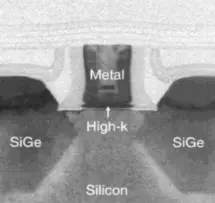
| + | Bonell is designed to be manufactured using a [[45 nm process]]. Intel's 45 nm process is the first high-volume manufacturing process to introduce High-k + metal gate transistors. | ||
| + | |||
| + | [[File:intel 45nm transistor.png|215px|left]] | ||
| + | {| class="wikitable" | ||
| + | |- | ||
| + | ! !! Bonnell | ||
| + | |- | ||
| + | | || [[45 nm]] | ||
| + | |- | ||
| + | | Gate Pitch || 180 nm | ||
| + | |- | ||
| + | | Interconnect Pitch || 160 nm | ||
| + | |- | ||
| + | | SRAM bit cell (HD) || 0.346 µm² | ||
| + | |- | ||
| + | | SRAM bit cell (LP) || 0.382 µm² | ||
| + | |} | ||
| + | {{clear}} | ||
| + | |||
== Architecture == | == Architecture == | ||
Bonnell features a brand new architecture not based on any previous Intel design. The architecture was specifically designed for ultra-mobile PCs (UMPCs), mobile internet devices (MID), and other embedded devices. Bonnell's primary goals were: | Bonnell features a brand new architecture not based on any previous Intel design. The architecture was specifically designed for ultra-mobile PCs (UMPCs), mobile internet devices (MID), and other embedded devices. Bonnell's primary goals were: | ||
Revision as of 00:30, 23 March 2017
| Edit Values | |
| Bonnell µarch | |
| General Info | |
| Arch Type | CPU |
| Designer | Intel |
| Manufacturer | Intel |
| Introduction | 2008 |
| Phase-out | 2011 |
| Process | 45 nm |
| Core Configs | 1, 2 |
| Pipeline | |
| Type | Superscalar, Superpipeline |
| Speculative | No |
| Reg Renaming | No |
| Stages | 16 |
| Instructions | |
| ISA | IA-32, x86-64 |
| Extensions | MOVBE, MMX, SSE, SSE2, SSE3, SSSE3 |
| Cache | |
| L1I Cache | 32 KiB/Core 8-way set associative |
| L1D Cache | 24 KiB/Core 6-way set associative |
| L2 Cache | 512 KiB/Core 8-way set associative |
| Cores | |
| Core Names | Silverthorne, Diamondville, Lincroft, Pineview, Tunnel Creek, Stellarton, Sodaville, Groveland |
| Succession | |
Bonnell was a microarchitecture for Intel's 45 nm ultra-low power microprocessors first introduced in 2008 for their then-new Atom family. Bonnell, which was named after the highest point in Austin - Mount Bonnell, was Intel's first x86-compatible microarchitecture designed to target the ultra-low power market.
Contents
Codenames
| Chipset | Platform | PHC | Core | Target |
|---|---|---|---|---|
| Poulsbo | Menlow | Silverthorne | MIDs | |
| Poulsbo | Menlow | Diamondville | Nettops | |
| Moorestown | Langwell | Lincroft | MIDs | |
| Pine Trail | Tiger Point | Pineview | Nettops | |
| Queens Bay | Topcliff | Tunnel Creek | Embedded | |
| Queens Bay | Topcliff | Stellarton | Embedded + Altera FPGA | |
| Sodaville | CE | |||
| Groveland | CE |
Generation successor
| First Generation | Second Generation | |
|---|---|---|
| Silverthorne | → | Lincroft |
| Diamondville | → | Pineview |
| Tunnel Creek | ||
| Stellarton | ||
| Sodaville | ||
| Groveland |
Release Dates
Bonnell was first announced on April 2nd 2008 during the Intel Developers Forum in Shanghai.
Process Technology
| 45 nm Manufacturing Fabs | |
|---|---|
| Fab | Location |
| D1D | Hillsboro, Oregon |
| Fab 32 | Chandler, Arizona |
| Fab 28 | Kiryat Gat, Israel |
Bonell is designed to be manufactured using a 45 nm process. Intel's 45 nm process is the first high-volume manufacturing process to introduce High-k + metal gate transistors.
| Bonnell | |
|---|---|
| 45 nm | |
| Gate Pitch | 180 nm |
| Interconnect Pitch | 160 nm |
| SRAM bit cell (HD) | 0.346 µm² |
| SRAM bit cell (LP) | 0.382 µm² |
Architecture
Bonnell features a brand new architecture not based on any previous Intel design. The architecture was specifically designed for ultra-mobile PCs (UMPCs), mobile internet devices (MID), and other embedded devices. Bonnell's primary goals were:
- Reduce power consumption,
- while staying fully x86-compatible,
- at acceptable performance
Performance/Power new rule: +1% performance for at most +1% power consumption.
Architecture
- Strictly ultra-low power
- 45 nm process, 9 metal layers, CMOS
- 500 mW to 2 W TDP
- 533 MT/s dual mode (GTL & CMOS) FSB
- In-order
- 2-issue decode
- Simple 2-way SMT
- Instruction Queue of 16 entries/thread
- FP Register File (per thread)
- Integer Register File (per thread)
- Private L1 cache for each core
- Shared L2 cache for the entire chip
The number of functional units were kept to minimum to cut on power consumption.
- 2 address generation units (AGUs)
- 2 Integer ALUs (1 for jumps, 1 for shifts)
- 2 FP ALUs (1 adder, 1 for others)
- No Integer multiplier & divider (shared with FP ALU instead)
Memory Hierarchy
- Cache
- Hardware prefetchers
- C6 cache
- 10.5 KiB array to hold the architectural state during deep power down state
- L1 Data Cache
- 32 KiB
- 8-way set associative
- 1 read and 1 write port
- 8 transistors (instead of 6) to reduce voltage
- L1 Instruction Cache
- 24 KiB
- 6-way set associative
- 1 read and 1 write port
- 8 transistors (instead of 6) to reduce voltage
- Per core
- L2 Cache:
- 512 KiB 8-way set associative
- ECC
- Shrinkable from 512 KiB to 128 KiB (2-way)
- Per core
- L3 Cache:
- No level 3 cache
- RAM
- Maximum of 2 GiB, 4 GiB, and 8 GiB
Note that the L1 cache for data and instructions were originally both 32 KiB (8-way), however due to power restrictions, the L1d$ was later reduced to 24 KiB.
Pipeline
Bonnell's architecture shares very little in common with other Intel designs. To achieve the strict ultra-low power objects, Bonnell features a very slimmed own design discarding many high-performance techniques used by Intel's high-performance architectures such as aggressive speculative execution, out-of-order execution, and µop transformation.
Bonnell consists of an in-order dual-issue 16-stage pipeline. Bonnell supports 2-way SMT
The longer pipeline allows a more evenly spreading of heat across the chip with more units. This also allows a higher clock rate.
- Instruction Fetch
- 3 stages
- 8 Bytes/Cycle (lower if SMT)
- Instruction Decode
- 3 stages
- Instructions with up to 3 prefixes/Cycle
- Instruction Dispatch
- 2 stages
- Source Operand Read
- 1 stage
- reading register operand
- 1 stage
- Data Cache Access
- 3 stages
- 1 stage for calculating
- 2 stages for reading cache
- 3 stages
- Execution
- 2 clusters
- integers
- quick cache access due to direct connection
- floating point & SIMD
- integers
- 2 clusters
- Exception & MT Handling
- 2 stages
- Commit
- 1 stage
Multithreading
Bonnell has support for multithreading - up to two threads per core. However each thread compete for the same resources which does inherently means they run slower than they would if they were to run alone.
Branch Prediction
- Two-level adaptive predictor
- 12-bit branch history register
- Pattern history table has 4096 entries (shared between threads)
- Branch buffer target has 128 entries (4-way, 32 sets)
- Unconditional jumps are ignored
- Always-taken and never-taken are marked in the table
- Penalties:
- 13 stages for miss prediction
- 7 stages for correct prediction but missing branch target buffer (BTB)
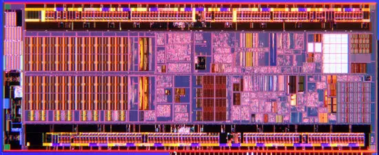
Die
- 45 nm process
- 9 metal layers
- 47,000,000 transistors
- 3.1 mm x 7.8 mm
- 24.2 mm² die size
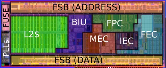
- BIC - Bus Interface Cluster
- MEC - Memory Cluster Execution & L1d$
- FPC - FP/SIMD execution Cluster
- IEC - Integer Execution Cluster
- FEC - Front-End Cluster & L1i$
- FSB - Front Side Bus
Cores
First Generation
First generation of Bonnell-based microprocessors introduced 2 cores: Silverthorne for ultra-mobile PCs and mobile Internet devices (MIDs) and Diamondville for ultra cheap notebooks and desktops.
Silverthorne
- Main article: Silverthorne
Silverthorne was the codename for a series of Mobile Internet Devices (MIDs) introduced in 2008. These processors had 1 core and 2 threads with a FSB operating at 400 MHz-533 MHz.
Diamondville
- Main article: Diamondville
Diamondville was the codename for the series of ultra cheap notebooks and desktops introduced in 2008. Diamondville is very much a soldered-on-motherboard derivative of Silverthorne with faster FSB (operating at 533 MHz - 667 MHz). The dual-core version is an MCM (Multi Chip Module) Silverthorne variant.
Second Generation
First generation of Bonnell-based microprocessors while being low power had to work with the older 90 nm process 945GSE chipset and 82801GBM I/O controller with a TDP of almost 9.5 watts - almost 4 times that of the processor itself. Second generation Bonnell-based microprocessors aimed to address this issue by integrating a memory controller and GPU on-chip. This drastically reduced power consumption and cost.
Lincroft
- Main article: Lincroft
Lincroft is the codename for Bonnell-based Silverthorne's successor. Lincroft integrates on-die the graphics and memory controller.
Pineview
- Main article: Pineview
Pineview was the codename for second generate Bonnell-based processors which integrated a memory controller, Direct Media Interface (DMI) link, and the GMA 3150 GPU. Pineview is the successor for Diamondville, targeting the same ultra cheap desktops, nettops and netbooks.
Tunnel Creek
- Main article: Tunnel Creek
Tunnel Creek was the codename for a series of MPUs for embedded applications.
Stellarton
- Main article: Stellarton
Stellarton was the codename for a series of MPUs for embedded applications. Stellarton is the Tunnel Creek core packaged with an Altera FPGA.
Sodaville
- Main article: Sodaville
Sodaville is the codename for a series of consumer electronics system on a chip (e.g. set-top box).
Groveland
- Main article: Groveland
Groveland is the codename for a series of consumer electronics MPUs (e.g. smart TVs).
All Bonnell Chips
| Bonnell Chips | ||||||||||
|---|---|---|---|---|---|---|---|---|---|---|
| CPU | IGP | |||||||||
| Model | µarch | Platform | Core | Launched | SDP | Freq | Max Mem | Name | Freq | Max Freq |
| 230 | Bonnell | Nettop 2008 | Diamondville | 3 June 2008 | 1,599.99 MHz 1.6 GHz 1,599,990 kHz | 8,192 MiB 8,388,608 KiB 8,589,934,592 B 8 GiB 0.00781 TiB | ||||
| 330 | Bonnell | Nettop 2008 | Diamondville | 21 September 2008 | 1,599.99 MHz 1.6 GHz 1,599,990 kHz | 8,192 MiB 8,388,608 KiB 8,589,934,592 B 8 GiB 0.00781 TiB | ||||
| N270 | Bonnell | Nettop 2008 | Diamondville | 3 June 2008 | 1,599.99 MHz 1.6 GHz 1,599,990 kHz | 8,192 MiB 8,388,608 KiB 8,589,934,592 B 8 GiB 0.00781 TiB | ||||
| N280 | Bonnell | Nettop 2008 | Diamondville | 7 February 2009 | 1,666.66 MHz 1.667 GHz 1,666,660 kHz | 8,192 MiB 8,388,608 KiB 8,589,934,592 B 8 GiB 0.00781 TiB | ||||
| Z500 | Bonnell | Menlow | Silverthorne | 2 April 2008 | 0.96 W 960 mW 0.00129 hp 9.6e-4 kW | 800 MHz 0.8 GHz 800,000 kHz | ||||
| Z510 | Bonnell | Menlow | Silverthorne | 2 April 2008 | 0.96 W 960 mW 0.00129 hp 9.6e-4 kW | 1,100 MHz 1.1 GHz 1,100,000 kHz | ||||
| Z510P | Bonnell | Menlow | Silverthorne | 2 March 2009 | 1,100 MHz 1.1 GHz 1,100,000 kHz | |||||
| Z510PT | Bonnell | Menlow | Silverthorne | 2 March 2009 | 1,100 MHz 1.1 GHz 1,100,000 kHz | |||||
| Z515 | Bonnell | Menlow | Silverthorne | 8 April 2009 | 1,200 MHz 1.2 GHz 1,200,000 kHz | |||||
| Z520 | Bonnell | Menlow | Silverthorne | 2 April 2008 | 0.96 W 960 mW 0.00129 hp 9.6e-4 kW | 1,333.33 MHz 1.333 GHz 1,333,330 kHz | ||||
| Z520PT | Bonnell | Menlow | Silverthorne | 2 March 2009 | 1,333.33 MHz 1.333 GHz 1,333,330 kHz | |||||
| Z530 | Bonnell | Menlow | Silverthorne | 2 April 2008 | 1,599.99 MHz 1.6 GHz 1,599,990 kHz | |||||
| Z530P | Bonnell | Menlow | Silverthorne | 2 March 2009 | 1,599.99 MHz 1.6 GHz 1,599,990 kHz | |||||
| Z540 | Bonnell | Menlow | Silverthorne | 2 April 2008 | 0.96 W 960 mW 0.00129 hp 9.6e-4 kW | 1,866.66 MHz 1.867 GHz 1,866,660 kHz | ||||
| Z550 | Bonnell | Menlow | Silverthorne | 8 April 2009 | 1,999.99 MHz 2 GHz 1,999,990 kHz | |||||
| Z560 | Bonnell | Menlow | Silverthorne | June 2010 | 2,133.33 MHz 2.133 GHz 2,133,330 kHz | |||||
| Z600 | Bonnell | Moorestown | Lincroft | 4 May 2010 | 800 MHz 0.8 GHz 800,000 kHz | 1,024 MiB 1,048,576 KiB 1,073,741,824 B 1 GiB 9.765625e-4 TiB | PowerVR SGX535 | 200 MHz 0.2 GHz 200,000 KHz | ||
| Z605 | Bonnell | Moorestown | Lincroft | 4 May 2010 | 1,000 MHz 1 GHz 1,000,000 kHz | 2,048 MiB 2,097,152 KiB 2,147,483,648 B 2 GiB 0.00195 TiB | PowerVR SGX535 | 400 MHz 0.4 GHz 400,000 KHz | ||
| Z610 | Bonnell | Moorestown | Lincroft | 4 May 2010 | 800 MHz 0.8 GHz 800,000 kHz | 2,048 MiB 2,097,152 KiB 2,147,483,648 B 2 GiB 0.00195 TiB | PowerVR SGX535 | 400 MHz 0.4 GHz 400,000 KHz | ||
| Z612 | Bonnell | Moorestown | Lincroft | 4 May 2010 | 900 MHz 0.9 GHz 900,000 kHz | 2,048 MiB 2,097,152 KiB 2,147,483,648 B 2 GiB 0.00195 TiB | PowerVR SGX535 | 400 MHz 0.4 GHz 400,000 KHz | ||
| Z615 | Bonnell | Moorestown | Lincroft | 4 May 2010 | 1,200 MHz 1.2 GHz 1,200,000 kHz | 2,048 MiB 2,097,152 KiB 2,147,483,648 B 2 GiB 0.00195 TiB | PowerVR SGX535 | 400 MHz 0.4 GHz 400,000 KHz | ||
| Z620 | Bonnell | Moorestown | Lincroft | 4 May 2010 | 900 MHz 0.9 GHz 900,000 kHz | 2,048 MiB 2,097,152 KiB 2,147,483,648 B 2 GiB 0.00195 TiB | PowerVR SGX535 | 400 MHz 0.4 GHz 400,000 KHz | ||
| Z625 | Bonnell | Moorestown | Lincroft | 4 May 2010 | 1,500 MHz 1.5 GHz 1,500,000 kHz | 2,048 MiB 2,097,152 KiB 2,147,483,648 B 2 GiB 0.00195 TiB | PowerVR SGX535 | 400 MHz 0.4 GHz 400,000 KHz | ||
| Z650 | Bonnell | Oak Trail | Lincroft | 11 April 2011 | 1,200 MHz 1.2 GHz 1,200,000 kHz | 2,048 MiB 2,097,152 KiB 2,147,483,648 B 2 GiB 0.00195 TiB | PowerVR SGX535 | 400 MHz 0.4 GHz 400,000 KHz | ||
| Z670 | Bonnell | Oak Trail | Lincroft | 11 April 2011 | 1,500 MHz 1.5 GHz 1,500,000 kHz | 2,048 MiB 2,097,152 KiB 2,147,483,648 B 2 GiB 0.00195 TiB | PowerVR SGX535 | 400 MHz 0.4 GHz 400,000 KHz | ||
| codename | Bonnell + |
| core count | 1 + and 2 + |
| designer | Intel + |
| first launched | 2008 + |
| full page name | intel/microarchitectures/bonnell + |
| instance of | microarchitecture + |
| instruction set architecture | IA-32 + and x86-64 + |
| manufacturer | Intel + |
| microarchitecture type | CPU + |
| name | Bonnell + |
| phase-out | 2011 + |
| pipeline stages | 16 + |
| process | 45 nm (0.045 μm, 4.5e-5 mm) + |


