(Remove gratuitous acromyms in wikilinks.) |
|||
| Line 203: | Line 203: | ||
{{empty section}} | {{empty section}} | ||
| − | ==== | + | ==== Gen10 ==== |
See {{intel|Gen10#Gen10|l=arch}}. | See {{intel|Gen10#Gen10|l=arch}}. | ||
| + | |||
| + | == Die == | ||
| + | === Dual-core === | ||
| + | * [[10 nm process]] | ||
| + | * [[13 metal layers]] | ||
| + | * ~8.2 mm x ~8.6 mm | ||
| + | * ~70.52 mm² die size | ||
| + | * 2 CPU cores + 40 GPU EUs | ||
== All Cannon Lake Chips == | == All Cannon Lake Chips == | ||
Revision as of 08:16, 16 June 2018
| Edit Values | |
| Cannon Lake µarch | |
| General Info | |
| Arch Type | CPU |
| Designer | Intel |
| Manufacturer | Intel |
| Introduction | May 15, 2018 |
| Process | 10 nm |
| Core Configs | 2 |
| Pipeline | |
| Type | Superscalar |
| OoOE | Yes |
| Speculative | Yes |
| Reg Renaming | Yes |
| Stages | 14-19 |
| Decode | 5-way? |
| Instructions | |
| ISA | x86-64 |
| Extensions | MOVBE, MMX, SSE, SSE2, SSE3, SSSE3, SSE4.1, SSE4.2, POPCNT, AVX, AVX2, AES, PCLMUL, FSGSBASE, RDRND, FMA3, F16C, BMI, BMI2, VT-x, VT-d, TXT, TSX, RDSEED, ADCX, PREFETCHW, CLFLUSHOPT, XSAVE, SGX, MPX, AVX-512, AVX-512F, AVX-512CD, AVX-512BW, AVX-512DQ, AVX-512VL, AVX-512IFMA, AVX-512VBMI, SHA, UMIP |
| Cache | |
| L1I Cache | 32 KiB/core 8-way set associative |
| L1D Cache | 32 KiB/core 8-way set associative |
| L2 Cache | 256 KiB/core 4-way set associative |
| L3 Cache | 2 MiB/core Up to 16-way set associative |
| Cores | |
| Core Names | Cannon Lake Y, Cannon Lake U |
| Succession | |
| Contemporary | |
| Coffee Lake | |
Cannon Lake (CNL) (formerly Skymont) is a planned microarchitecture by Intel as a successor to Kaby Lake. Cannon Lake is expected to be fabricated using a 10 nm process and is set to be introduced in the second half of 2018. Cannon Lake is the "Process" microarchitecture as part of Intel's PAO model.
For mobile, Cannon Lake is expected to be branded as 8th Generation Intel Core i3, Core i5. and Core i7 processors.
Contents
Codenames
| Core | Abbrev | Description | Graphics | Target |
|---|---|---|---|---|
| Cannon Lake Y | CNL-Y | Extremely low power | GT2 | 2-in-1s detachable, tablets, and computer sticks |
| Cannon Lake U | CNL-U | Ultra-low Power | GT2/GT3 | Light notebooks, portable All-in-Ones (AiOs), Minis, and conference room |
| Cannon Lake H | CNL-H | High-performance Graphics | GT2/GT3 | Ultimate mobile performance, mobile workstations |
| Cannon Lake S | CNL-S | Performance-optimized lifestyle | GT2/GT3 | Desktop performance to value, AiOs, and minis |
| Cannon Lake DT | CNL-DT | Workstation | GT2 | Workstations & entry-level servers |
Release Dates
Initial Cannon Lake models were introduced in May 2018 with additional models planned throughout the year.
Process Technology
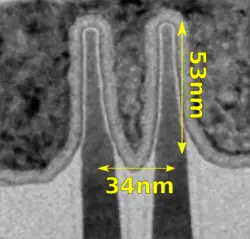
Cannon Lake is manufactured on Intel's 10 nm process (P1274). Intel's 10 nm process is among the first high-volume manufacturing processes to employ Self-Aligned Quad Patterning (SAQP) (goes under the "Hyper-Scaling" marketing name). Intel's 10nm features a 0.0367 µm² SRAM bit cell.
| Broadwell | Cannon Lake | Δ | 
| |
|---|---|---|---|---|
| 14 nm | 10 nm | |||
| Fin Pitch | 42 nm | 34 | 0.81x | |
| Fin Width | 8 nm | 7 nm | 0.88x | |
| Fin Height | 42 nm | 53 nm | 1.24x | |
| Gate Pitch | 70 nm | 54 nm | 0.77x | |
| Interconnect Pitch | 52 nm | 36 nm | 0.69x | |
| Cell Height | 399 nm | 272 nm | 0.68x |
Compiler support
Support for Cannon Lake was added in GCC 8.1 and LLVM 6.0.
| Compiler | Arch-Specific | Arch-Favorable |
|---|---|---|
| ICC | -march=cannonlake |
-mtune=cannonlake
|
| GCC | -march=cannonlake |
-mtune=cannonlake
|
| LLVM | -march=cannonlake |
-mtune=cannonlake
|
| Visual Studio | ? |
?
|
CPUID
| Core | Extended Family |
Family | Extended Model |
Model |
|---|---|---|---|---|
| Y, U | 0 | 0x6 | 0x6 | 0x6 |
| Family 6 Model 102 | ||||
Architecture
| This section is empty; you can help add the missing info by editing this page. |
Key changes from Skylake/Kaby Lake/Coffee Lake
- 10 nm process (from 14 nm)
- Mainstream chipset
- Mobile Processors
- LPDDR4/LPDDR4X memory support (from LPDDR3)
- Rates up to 2400 MT/s
- LPDDR4/LPDDR4X memory support (from LPDDR3)
- Gen9.5 → Gen10 graphics
- Gen10 GPUs
- HD Graphics 610 → UHD Graphics 710 (24 Execution Units, 2x EUs from Kaby Lake)
- HD Graphics 615 → UHD Graphics 715 (40 Execution Units, 1.7x EUs from Kaby Lake)
- HD Graphics 620 → UHD Graphics 720 (40 Execution Units, 1.7x EUs from Kaby Lake)
- HD Graphics 630 → UHD Graphics 730 (40 Execution Units, 1.7x EUs from Kaby Lake)
- HD Graphics P630 → UHD Graphics P730 (40 Execution Units, 1.7x EUs from Kaby Lake)
- Iris Plus Graphics 640 → Iris Plus Graphics 740 (unknown change)
- Iris Plus Graphics 650 → Iris Plus Graphics 750 (unknown change)
New instructions
Cannon Lake introduced a number of new instructions:
-
AVX-512, specifically:-
AVX512F- AVX-512 Foundation -
AVX512CD- AVX-512 Conflict Detection -
AVX512BW- AVX-512 Byte and Word -
AVX512DQ- AVX-512 Doubleword and Quadword -
AVX512VL- AVX-512 Vector Length -
AVX512IFMA- AVX-512 Integer Fused Multiply-Add -
AVX512VBMI- AVX-512 Vector Bit Manipulation
-
-
SHA- Hardware acceleration for SHA hashing operations -
UMIP- User-Mode Instruction Prevention extension
Block Diagram
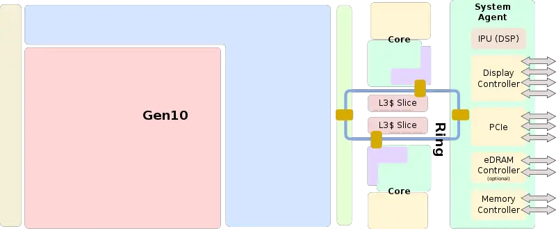
Entire SoC Overview (dual)
Individual Core
| This section is empty; you can help add the missing info by editing this page. |
Gen10
See Gen10#Gen10.
Die
Dual-core
- 10 nm process
- 13 metal layers
- ~8.2 mm x ~8.6 mm
- ~70.52 mm² die size
- 2 CPU cores + 40 GPU EUs
All Cannon Lake Chips
| Cannon Lake Chips | |||||||||||||||||||||||
|---|---|---|---|---|---|---|---|---|---|---|---|---|---|---|---|---|---|---|---|---|---|---|---|
| Main processor | IGP | Major Feature Diff | |||||||||||||||||||||
| Model | Launched | Price | Family | Platform | Core | C | T | L3$ | L4$ | TDP | Freq | Turbo | Max Mem | Name | Freq | Turbo | TBT | HT | AVX2 | TXT | TSX | vPro | VT-d |
| M3-8114Y | Core M3 | Cannon Lake Y | 2 | 4 | 1.5 GHz 1,500 MHz 1,500,000 kHz | 16 GiB 16,384 MiB 16,777,216 KiB 17,179,869,184 B 0.0156 TiB | UHD Graphics ? | 300 MHz 0.3 GHz 300,000 KHz | ✔ | ✔ | ✔ | ✘ | ✘ | ✘ | ✔ | ||||||||
| i3-8121U | 15 May 2018 | Core i3 | Cannon Lake U | 2 | 4 | 4 MiB 4,096 KiB 4,194,304 B 0.00391 GiB | 15 W 15,000 mW 0.0201 hp 0.015 kW | 2.2 GHz 2,200 MHz 2,200,000 kHz | 3.2 GHz 3,200 MHz 3,200,000 kHz | 32 GiB 32,768 MiB 33,554,432 KiB 34,359,738,368 B 0.0313 TiB | ✔ | ✔ | ✔ | ✘ | ✘ | ✘ | ✔ | ||||||
| Count: 2 | |||||||||||||||||||||||
References
- Mark Bohr, Intel. Intel Technology and Manufacturing Day. Mar 28, 2017.
See also
- AMD's Zen
| codename | Cannon Lake + |
| core count | 2 + |
| designer | Intel + |
| first launched | May 15, 2018 + |
| full page name | intel/microarchitectures/cannon lake + |
| instance of | microarchitecture + |
| instruction set architecture | x86-64 + |
| manufacturer | Intel + |
| microarchitecture type | CPU + |
| name | Cannon Lake + |
| pipeline stages (max) | 19 + |
| pipeline stages (min) | 14 + |
| process | 10 nm (0.01 μm, 1.0e-5 mm) + |
