(→Front End) |
(→Front End) |
||
| Line 243: | Line 243: | ||
==== Front End ==== | ==== Front End ==== | ||
| − | [[File:amd zen hc28 fetch.png| | + | [[File:amd zen hc28 fetch.png|300px|right]] |
The Front End of the Zen core deals with the [[in-order]] operations such as [[instruction fetch]] and [[instruction decode]]. The instruction fetch is composed of two paths: a traditional decode path where instructions come from the [[instruction cache]] and a [[µOPs cache]] that are determined by the [[branch prediction]] (BP) unit. | The Front End of the Zen core deals with the [[in-order]] operations such as [[instruction fetch]] and [[instruction decode]]. The instruction fetch is composed of two paths: a traditional decode path where instructions come from the [[instruction cache]] and a [[µOPs cache]] that are determined by the [[branch prediction]] (BP) unit. | ||
| − | The | + | The [[branch prediction]] unit is decoupled and can start working as soon as it receives a desired operation such as a redirect, ahead of traditional instruction fetches. AMD still uses a [[perceptron branch predictor|hashed perceptron system]] similar to the one used in {{\\|Jaguar}} and {{\\|Bobcat}}, albeit likely much more finely tuned. AMD stated it's also larger than previous architectures but did not disclose actual sizes. The TLB in the BP pipe was moved up to much earlier in the pipe so that the physical address could be retrieved at an earlier stage and prefetched ahead of time. The BP is capable of storing 2 branches per BTB (Branch Target Buffer) entry, reducing the number of BTB reads necessary. The BP includes a 32-entry return stack and has an Indirect Target Array (ITA) for indirect target operations. The BP TLB is composed of: |
* 8-entry L0 TLB, all page sizes | * 8-entry L0 TLB, all page sizes | ||
| Line 253: | Line 253: | ||
Instructions are fetched from the [[L2 cache]] at the rate of 32B/cycle. Zen does not have an even [[L1$]]. The [[instruction cache]] is 64 [[KiB]], double that of the data cache. Depending on the branch prediction decision instructions may be fetched from the instruction cache or from the µOPs in which case costly decoding will be avoided. | Instructions are fetched from the [[L2 cache]] at the rate of 32B/cycle. Zen does not have an even [[L1$]]. The [[instruction cache]] is 64 [[KiB]], double that of the data cache. Depending on the branch prediction decision instructions may be fetched from the instruction cache or from the µOPs in which case costly decoding will be avoided. | ||
| + | [[File:amd zen hc28 decode.png|left|300px]] | ||
| + | On the traditional side of decode instructions are fetched from the L1$ at 32B/cycle and go to the instruction byte buffer and through the pick stage to the decode. The decode allows for 4 [[x86]] instructions to be decoded per cycle which are in turn sent to the µOP Queue. Ideally, most instructions get a hit from the BP and acquire a µOP tag, sending them directly to be retrieved from the µOP cache which are then sent to the µOP Queue. This bypasses most of the expensive fetching and decoding that would otherwise be needed to be done. At this stage of the pipeline, Zen performs additional optimizations such as branch fusion - an operation where a comparison and branch op gets combined into a single µOP (resulting in a single schedule+single execute). | ||
| + | |||
| + | At the decode stage Zen incorporates the [[microcode]] ROM and the Stack Engine Memfile (SEM). The new Memfile sits between the queue and dispatch monitoring the µOP traffic. The Memfile is capable of performing [[store-to-load forwarding]] right at dispatch for loads that trail behind known stores with physical addresses. This is a low-power solution that off-loads some of the work that is usually done by the [[AGU]]. | ||
| + | |||
| + | Dispatch is capable of sending up to 6 µOPs to [[Integer]] EX and an additional 4 µOPs to the [[Floating Point]] (FP) EX. Zen can dispatch to both at the same time (i.e. for a maximum of 10 µOPs per cycle). | ||
==== Execution Engine ==== | ==== Execution Engine ==== | ||
Revision as of 02:44, 30 January 2017
| Edit Values | |
| Zen µarch | |
| General Info | |
| Arch Type | CPU |
| Designer | AMD |
| Manufacturer | GlobalFoundries |
| Introduction | 2017 |
| Process | 14 nm |
| Core Configs | 2, 4, 8, 16, 32 |
| Pipeline | |
| Type | Superscalar |
| Speculative | Yes |
| Reg Renaming | Yes |
| Instructions | |
| ISA | x86-16, x86-32, x86-64 |
| Extensions | MOVBE, MMX, SSE, SSE2, SSE3, SSSE3, SSE4.1, SSE4.2, POPCNT, AVX, AVX2, AES, PCLMUL, RDRND, F16C, BMI, BMI2, RDSEED, ADCX, PREFETCHW, CLFLUSHOPT, XSAVE, SHA, CLZERO |
| Cache | |
| L1I Cache | 64 KiB/core 4-way set associative |
| L1D Cache | 32 KiB/core 8-way set associative |
| L2 Cache | 512 KiB/core 8-way set associative |
| L3 Cache | 2 MiB/core Up to 16-way set associative |
| Cores | |
| Core Names | Raven Ridge, Summit Ridge, Snowy Owl, Naples |
| Succession | |
Zen (family 17h) is the microarchitecture developed by AMD as a successor to both Excavator and Puma. Zen is an entirely new design, built from the ground up for optimal balance of performance and power capable of covering the entire computing spectrum from fanless notebooks to high-performance desktop computers. Zen is set to be released in early-2017. Zen is set to be eventually replaced by Zen+.
Contents
Etymology
Zen was picked by Michael Clark, AMD's senior fellow and lead architect. Zen was picked to represent the balance needed between the various competing aspects of a microprocessor - transistor allocation/die size, clock/frequency restriction, power limitations, and new instructions to implement.
Codenames
| Core | C/T | Target |
|---|---|---|
| Naples | 32/64 | High-end server multiprocessors |
| Snowy Owl | 16/32 | Mid-range server processors |
| Summit Ridge | 8/16 | High-end desktops & enthusiasts market |
| Raven Ridge | 4/8 | Mainstream desktop & mobile processors with GPU |
Brands
| This section is empty; you can help add the missing info by editing this page. |
Release Dates
The first set of processors, as part of the Ryzen family is expected to be officially launched before the end of Q1 - likely mid-February 2017 before the Game Developer Conference (GDC). Server processors are set to be released in by the end of Q2, 2017. Mobile processors are expected to be released by the end of 2017.
Process Technology
Zen is planned to be manufactured on Global Foundries' 14 nm process. AMD's previous microarchitectures were based on 32 and 28 nanometer processes. The jump to 14 nm is part of AMD attempt to remain competitive against Intel (Both SkyLake and Kaby Lake are also manufactured on 14 nm although by 2017 Intel plans on moving on to Cannonlake and 10 nm process). The move to 14 nm will bring along related benefits of a smaller node such as reduced heat and power consumption for identical designs.
Compatibility
Microsoft announced that only Windows 10 will have support for Zen. Linux added initial support for Zen starting with Linux Kernel 4.1.
| Vendor | OS | Version | Notes |
|---|---|---|---|
| Microsoft | Windows | Windows 7 | No Support |
| Windows 8 | No Support | ||
| Windows 10 | Support | ||
| Linux | Linux | Kernel 4.1 | Initial Support |
Compiler support
| Compiler | Arch-Specific | Arch-Favorable |
|---|---|---|
| GCC | -march=znver1 |
-mtune=znver1
|
| LLVM | -march=znver1 |
-mtune=znver1
|
| Visual Studio | /arch:AVX2 |
? |
Architecture
AMD Zen is an entirely new design from the ground up which introduces considerable amount of improvements and design changes over Excavator. Zen-based microprocessors will utilize AMD's Socket AM4 unified platform.
Key changes from Excavator
- Zen was designed to succeed BOTH Excavator (High-performance) and Puma (Low-power) covering the entire range in one architecture
- Cover the entire spectrum from fanless notebooks to high-performance desktops
- More aggressive clock gating with multi-level regions
- Power focus from design, employs low-power design methodologies
- Utilizes 14 nm process (from 28 nm)
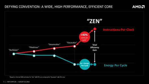
- 40% improvement in IPC per core per single-thread (From Excavator)
- Core engine
- SMT support, 2 threads/core
- Improved branch mispredictions
- Better branch predicitons with 2 branches per BTB entry
- Lower miss latency penalty
- Large Op cache
- Wider μop dispatch (6, up from 4)
- Larger instruction scheduler
- Integer (84, up form 48)
- Floating Point (96, up form 60)
- Larger retire throughput (8, up from 4)
- Larger Retire Queue (192, up from 128)
- Larger Load Queue (72, up from 44)
- Larger Store Queue (44, up from 32)
- Quad-issue FPU
- Cache system
- Write-back L1 cache eviction policy (From write-through)
- Faster L2 cache
- Faster L3 cache
- Large Op cache
- Faster Load to FPU (down to 7, from 9 cycles)
- Better L1$ and L2$ data prefetcher
- 2x the L1 and L2 bandwidth
- 5x L3 bandwidth
- Move elimination block added
New instructions
Zen introduced a number of new x86 instructions:
-
ADX- Multi-Precision Add-Carry Instruction extension -
RdRand- Hardware-based RNG -
SMAP- Supervisor Mode Access Prevention -
SHA- SHA extensions -
CLFLUSHOPT- Flush Cache Line -
XSAVE- Privileged Save/Restore -
CLZERO- Zero-out Cache Line (AMD exclusive)
Block Diagram
Individual Core
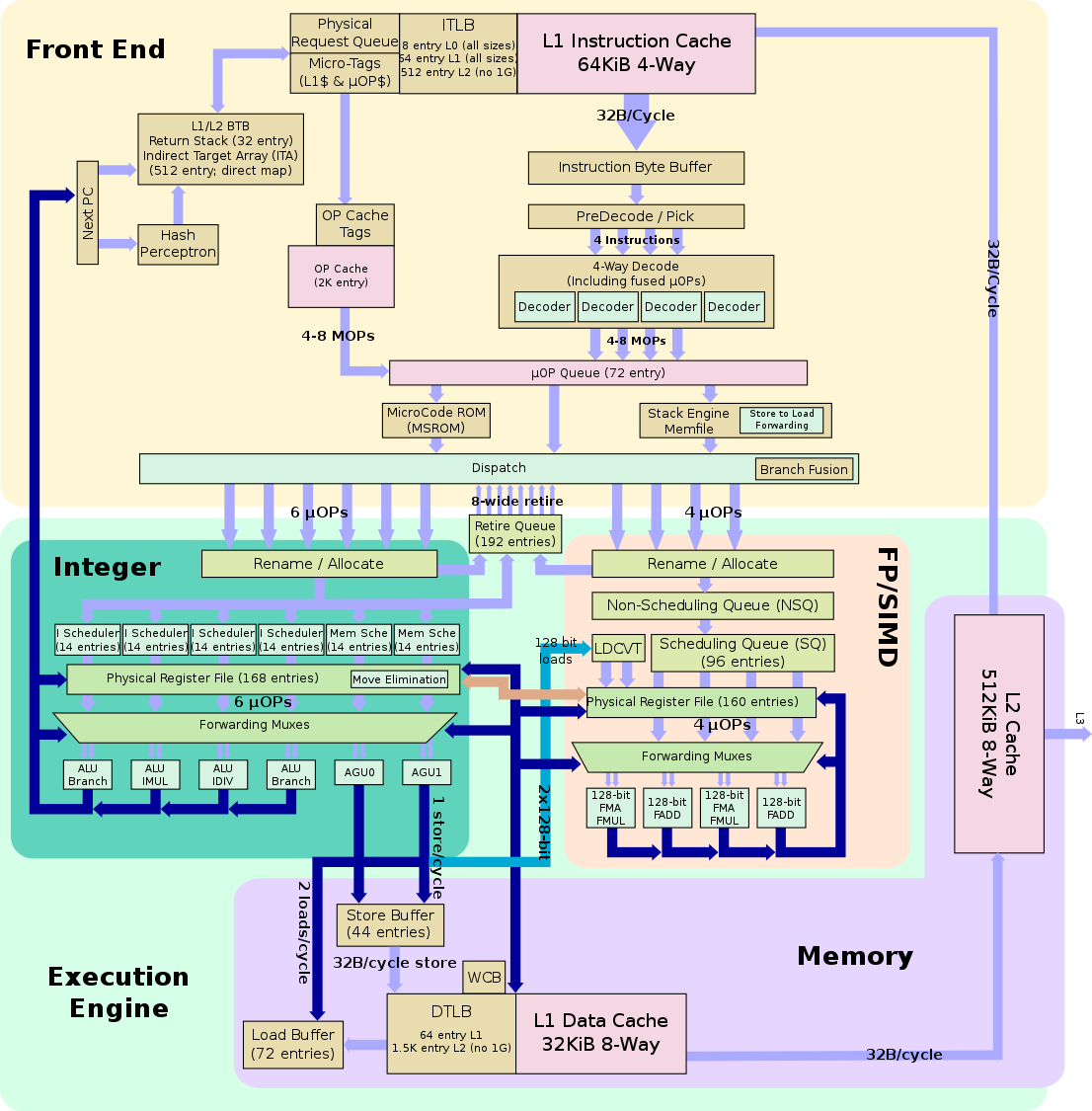
Memory Hierarchy
- Cache
- L1I Cache:
- 64 KiB 4-way set associative
- 32 B line size
- shared by the two threads, per core
- 64 KiB 4-way set associative
- L1D Cache:
- 32 KiB 8-way set associative
- 32 B line size
- write-back policy
- 32 KiB 8-way set associative
- L2 Cache:
- 512 KiB 8-way set associative
- 32 B line
- write-back policy
- L3 Cache:
- 2 MiB/core, shared across all cores.
- Up to 16-way set associative
- Write-back policy
- System DRAM:
- 2 Channels
- L1I Cache:
Zen TLB consists of dedicated level one TLB for instruction cache and another one for data cache. Additionally there is a unified second level TLB.
- TLBs
- BP TLB
- 8 entry L0 TLB, all page sizes
- 64 entry L1 TLB, all page sizes
- 512 entry L2 TLB, no 1G pages
- DTLB
- 64 entry, all page sizes
- STLB
- 1.5K entry, no 1G pages
- BP TLB
Pipeline
Zen presents a major design departure from the previous couple of microarchitectures. In the pursuit of remaining competitive against Intel, AMD went with a similar approach to Intel's: large beefier core with SoC design that can scale from extremely low TDP (fanless devices) to supercomputers utilizing dozens of cores. As such, Zen is aimed at replacing both Excavator (AMD's previous performance microarchitecture) and Puma (AMD's previous ultra-low power arch). In addition to covering the entire computing spectrum through power efficiency and core scalability, another major design goal was 40% uplift in single-thread performance (i.e. 40% IPC increase) from Excavator. The large increase in performance is the result of major redesigns in all four areas of the core (the front end, the execution engine, and the memory subsystem) as well as Zen's new SoC CCX (CPU Complex) modular design. The core itself is wider and all around bigger (roughly every component had its capacity substantially increased). The improvement in power efficiency is the result of the 14 nm process used as well as many low-power design methodologies that were utilized early on in the design process (Excavator has been manufactured on GF's 28 nm process). AMD introduced various components (such as their new prediction flow and forwarding mechanisms) that eliminate the need for operations to go through the high power ALUs and decoders, increasing the overall power efficiency and throughput.
Broad Overview
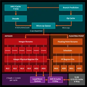
At a very broad view, Zen shares some similarities with its predecessor but introduces new elements and major changes. Each core is composed of a front end (in-order area) that fetches instructions, decodes them, generates µOPs and fused µOPs, and sends them to the Execution Engine (out-of-order section). Instructions are either fetched from the L1I$ or come from the µOPs cache (on subsequent fetches) eliminating the decoding stage altogether. Zen decodes 4 instructions/cycle into the µOP Queue. The µOP Queue dispatches separate µOPs to the Integer side and the FP side (dispatching to both at the same time when possible).
Unlike many of Intel's recent microarchitectures (such as Skylake and Kaby Lake) which make use of a unified scheduler, AMD continue to use a split pipeline design. µOP are decoupled at the µOP Queue and are sent through the two distinct pipelines to either the Integer side or the FP side. The two sections are completely separate, each featuring separate schedulers, queues, and execution units. The Integer side splits up the µOPs via a set of individual schedulers that feed the various ALU units. On the floating point side, there is a different scheduler to handle the 128-bit FP operations. Zen support all modern x86 extensions including AVX/AVX2, BMI1/BMI2, and AES. Zen also supports SHA, secure hash implementation instructions that are currently only found in Intel's ultra-low power microarchitectures (e.g. Goldmont) but not in their mainstream processors.
From the memory subsystem point of view, data is fed into the execution units from the L1D$ via the load and store queue (both of which were almost doubled in capacity) via the two Address Generation Units (AGUs) at the rate of 2 loads and 1 store per cycle. Each core also has a 512 KiB level 2 cache. L2 feeds both the the level 1 data and level 1 instruction caches at 32B per cycle. L2 is connected to the L3 cache which is shared across all cores.
Front End
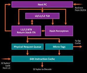
The Front End of the Zen core deals with the in-order operations such as instruction fetch and instruction decode. The instruction fetch is composed of two paths: a traditional decode path where instructions come from the instruction cache and a µOPs cache that are determined by the branch prediction (BP) unit.
The branch prediction unit is decoupled and can start working as soon as it receives a desired operation such as a redirect, ahead of traditional instruction fetches. AMD still uses a hashed perceptron system similar to the one used in Jaguar and Bobcat, albeit likely much more finely tuned. AMD stated it's also larger than previous architectures but did not disclose actual sizes. The TLB in the BP pipe was moved up to much earlier in the pipe so that the physical address could be retrieved at an earlier stage and prefetched ahead of time. The BP is capable of storing 2 branches per BTB (Branch Target Buffer) entry, reducing the number of BTB reads necessary. The BP includes a 32-entry return stack and has an Indirect Target Array (ITA) for indirect target operations. The BP TLB is composed of:
- 8-entry L0 TLB, all page sizes
- 64-entry L1 TLB, all page sizes
- 512-entry L2 TLB, no 1G pages
Instructions are fetched from the L2 cache at the rate of 32B/cycle. Zen does not have an even L1$. The instruction cache is 64 KiB, double that of the data cache. Depending on the branch prediction decision instructions may be fetched from the instruction cache or from the µOPs in which case costly decoding will be avoided.
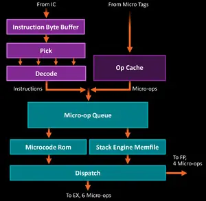
On the traditional side of decode instructions are fetched from the L1$ at 32B/cycle and go to the instruction byte buffer and through the pick stage to the decode. The decode allows for 4 x86 instructions to be decoded per cycle which are in turn sent to the µOP Queue. Ideally, most instructions get a hit from the BP and acquire a µOP tag, sending them directly to be retrieved from the µOP cache which are then sent to the µOP Queue. This bypasses most of the expensive fetching and decoding that would otherwise be needed to be done. At this stage of the pipeline, Zen performs additional optimizations such as branch fusion - an operation where a comparison and branch op gets combined into a single µOP (resulting in a single schedule+single execute).
At the decode stage Zen incorporates the microcode ROM and the Stack Engine Memfile (SEM). The new Memfile sits between the queue and dispatch monitoring the µOP traffic. The Memfile is capable of performing store-to-load forwarding right at dispatch for loads that trail behind known stores with physical addresses. This is a low-power solution that off-loads some of the work that is usually done by the AGU.
Dispatch is capable of sending up to 6 µOPs to Integer EX and an additional 4 µOPs to the Floating Point (FP) EX. Zen can dispatch to both at the same time (i.e. for a maximum of 10 µOPs per cycle).
Execution Engine
| This section is empty; you can help add the missing info by editing this page. |
Integer
| This section is empty; you can help add the missing info by editing this page. |
Floating Point
| This section is empty; you can help add the missing info by editing this page. |
Memory Subsystem
| This section is empty; you can help add the missing info by editing this page. |
Sockets/Platform
All Zen-based microprocessors utilizes AMD's Socket AM4, a unified socket infrastructure.
| Socket AM4 Platform [Edit] | ||||||||||
|---|---|---|---|---|---|---|---|---|---|---|
| Segment | Chipset | USB | SATA | SATAe | PCIe | RAID | Dual PCIe | Overclocking | ||
| 3.1 G1 | 3.1 G2 | 2.0 | ||||||||
| 500-series (Zen+, Zen 2, Zen 3) | ||||||||||
| Mainstream | B550 | 2 | 6 | 6 | 8 + 4x NVME | 0 | 16x Gen4 | 0,1,10 | ✔ | ✔ |
| Enthusiast | X570 | 0 | 8 | 4 | 14 + 4x NVME | 0 | 16x Gen4 | 0,1,10 | ||
| 400-series (Zen+) | ||||||||||
| Mainstream | B450 | 2 | 2 | 6 | 6 + 4x NVME | 1 | 6x Gen3 | 0,1,10 | ✘ | ✔ |
| Enthusiast | X470 | 6 | 2 | 6 | 10 + 4x NVME | 2 | 8x Gen3 | 0,1,10 | ✔ | |
| 300-series (Zen) | ||||||||||
| Small Form Factor | A300, B300 | 4 | 0 | 0 | 2 + 2x NVMe | 1 | 4x Gen3 | 0,1 | ✘ | |
| X300 | 4 | 0 | 0 | 2 + 2x NVMe | 1 | 4x Gen3 | 0,1 | ✔ | ||
| Entry-level | A320 | 6 | 1 | 6 | 4 + 2x NVMe | 2 | 4x Gen2 | 0,1,10 | ✘ | ✘ |
| Mainstream | B350 | 6 | 2 | 6 | 4 + 2x NVMe | 2 | 6x Gen2 | 0,1,10 | ✔ | |
| Enthusiast | X370 | 6 | 2 | 6 | 6 + 2x NVMe | 2 | 8x Gen2 | 0,1,10 | ✔ | |
Die Shot
| This section is empty; you can help add the missing info by editing this page. |
All Zen Chips
| Zen Chips | ||||||
|---|---|---|---|---|---|---|
| Model | Family | Core | Launched | Power Dissipation | Freq | Max Mem |
| 200GE | Athlon | Raven Ridge | 6 September 2018 | 3,200 MHz 3.2 GHz 3,200,000 kHz | 65,536 MiB 67,108,864 KiB 68,719,476,736 B 64 GiB 0.0625 TiB | |
| 220GE | Athlon | Raven Ridge | 21 December 2018 | 3,400 MHz 3.4 GHz 3,400,000 kHz | 65,536 MiB 67,108,864 KiB 68,719,476,736 B 64 GiB 0.0625 TiB | |
| 240GE | Athlon | Raven Ridge | 21 December 2018 | 3,500 MHz 3.5 GHz 3,500,000 kHz | 65,536 MiB 67,108,864 KiB 68,719,476,736 B 64 GiB 0.0625 TiB | |
| 3000G | Athlon | Dali Raven Ridge | 20 November 2019 | 3,500 MHz 3.5 GHz 3,500,000 kHz | 65,536 MiB 67,108,864 KiB 68,719,476,736 B 64 GiB 0.0625 TiB | |
| 300U | Athlon | Picasso | 6 January 2019 | 2,400 MHz 2.4 GHz 2,400,000 kHz | 65,536 MiB 67,108,864 KiB 68,719,476,736 B 64 GiB 0.0625 TiB | |
| 3150U | Athlon Gold | Dali | 6 January 2020 | 2,400 MHz 2.4 GHz 2,400,000 kHz | 32,768 MiB 33,554,432 KiB 34,359,738,368 B 32 GiB 0.0313 TiB | |
| PRO 200GE | Athlon | Raven Ridge | 6 September 2018 | 3,200 MHz 3.2 GHz 3,200,000 kHz | 65,536 MiB 67,108,864 KiB 68,719,476,736 B 64 GiB 0.0625 TiB | |
| 3050U | Athlon Silver | Dali | 6 January 2020 | 2,300 MHz 2.3 GHz 2,300,000 kHz | 32,768 MiB 33,554,432 KiB 34,359,738,368 B 32 GiB 0.0313 TiB | |
| 7251 | EPYC | Naples | 20 June 2017 | 2,100 MHz 2.1 GHz 2,100,000 kHz | 2,097,152 MiB 2,147,483,648 KiB 2,199,023,255,552 B 2,048 GiB 2 TiB | |
| 7261 | EPYC | Naples | 14 June 2018 | 2,500 MHz 2.5 GHz 2,500,000 kHz | 2,097,152 MiB 2,147,483,648 KiB 2,199,023,255,552 B 2,048 GiB 2 TiB | |
| 7281 | EPYC | Naples | 20 June 2017 | 2,100 MHz 2.1 GHz 2,100,000 kHz | 2,097,152 MiB 2,147,483,648 KiB 2,199,023,255,552 B 2,048 GiB 2 TiB | |
| 7301 | EPYC | Naples | 20 June 2017 | 2,200 MHz 2.2 GHz 2,200,000 kHz | 2,097,152 MiB 2,147,483,648 KiB 2,199,023,255,552 B 2,048 GiB 2 TiB | |
| 7351 | EPYC | Naples | 20 June 2017 | 2,400 MHz 2.4 GHz 2,400,000 kHz | 2,097,152 MiB 2,147,483,648 KiB 2,199,023,255,552 B 2,048 GiB 2 TiB | |
| 7351P | EPYC | Naples | 20 June 2017 | 2,400 MHz 2.4 GHz 2,400,000 kHz | 2,097,152 MiB 2,147,483,648 KiB 2,199,023,255,552 B 2,048 GiB 2 TiB | |
| 7371 | EPYC | Naples | 2019 | 3,100 MHz 3.1 GHz 3,100,000 kHz | 2,097,152 MiB 2,147,483,648 KiB 2,199,023,255,552 B 2,048 GiB 2 TiB | |
| 7401 | EPYC | Naples | 20 June 2017 | 2,000 MHz 2 GHz 2,000,000 kHz | 2,097,152 MiB 2,147,483,648 KiB 2,199,023,255,552 B 2,048 GiB 2 TiB | |
| 7401P | EPYC | Naples | 20 June 2017 | 2,000 MHz 2 GHz 2,000,000 kHz | 2,097,152 MiB 2,147,483,648 KiB 2,199,023,255,552 B 2,048 GiB 2 TiB | |
| 7451 | EPYC | Naples | 20 June 2017 | 2,300 MHz 2.3 GHz 2,300,000 kHz | 2,097,152 MiB 2,147,483,648 KiB 2,199,023,255,552 B 2,048 GiB 2 TiB | |
| 7501 | EPYC | Naples | 20 June 2017 | 2,000 MHz 2 GHz 2,000,000 kHz | 2,097,152 MiB 2,147,483,648 KiB 2,199,023,255,552 B 2,048 GiB 2 TiB | |
| 7551 | EPYC | Naples | 20 June 2017 | 2,000 MHz 2 GHz 2,000,000 kHz | 2,097,152 MiB 2,147,483,648 KiB 2,199,023,255,552 B 2,048 GiB 2 TiB | |
| 7551P | EPYC | Naples | 20 June 2017 | 2,000 MHz 2 GHz 2,000,000 kHz | 2,097,152 MiB 2,147,483,648 KiB 2,199,023,255,552 B 2,048 GiB 2 TiB | |
| 7601 | EPYC | Naples | 20 June 2017 | 2,200 MHz 2.2 GHz 2,200,000 kHz | 2,097,152 MiB 2,147,483,648 KiB 2,199,023,255,552 B 2,048 GiB 2 TiB | |
| 3101 | EPYC Embedded | Snowy Owl | 21 February 2018 | 2,100 MHz 2.1 GHz 2,100,000 kHz | 524,288 MiB 536,870,912 KiB 549,755,813,888 B 512 GiB 0.5 TiB | |
| 3151 | EPYC Embedded | Snowy Owl | 21 February 2018 | 2,700 MHz 2.7 GHz 2,700,000 kHz | 524,288 MiB 536,870,912 KiB 549,755,813,888 B 512 GiB 0.5 TiB | |
| 3201 | EPYC Embedded | Snowy Owl | 21 February 2018 | 1,500 MHz 1.5 GHz 1,500,000 kHz | 524,288 MiB 536,870,912 KiB 549,755,813,888 B 512 GiB 0.5 TiB | |
| 3251 | EPYC Embedded | Snowy Owl | 21 February 2018 | 2,500 MHz 2.5 GHz 2,500,000 kHz | 524,288 MiB 536,870,912 KiB 549,755,813,888 B 512 GiB 0.5 TiB | |
| 3255 | EPYC Embedded | Snowy Owl | 2,500 MHz 2.5 GHz 2,500,000 kHz | 524,288 MiB 536,870,912 KiB 549,755,813,888 B 512 GiB 0.5 TiB | ||
| 3301 | EPYC Embedded | Snowy Owl | 21 February 2018 | 2,000 MHz 2 GHz 2,000,000 kHz | 1,048,576 MiB 1,073,741,824 KiB 1,099,511,627,776 B 1,024 GiB 1 TiB | |
| 3351 | EPYC Embedded | Snowy Owl | 21 February 2018 | 1,900 MHz 1.9 GHz 1,900,000 kHz | 1,048,576 MiB 1,073,741,824 KiB 1,099,511,627,776 B 1,024 GiB 1 TiB | |
| 3401 | EPYC Embedded | Snowy Owl | 21 February 2018 | 1,850 MHz 1.85 GHz 1,850,000 kHz | 1,048,576 MiB 1,073,741,824 KiB 1,099,511,627,776 B 1,024 GiB 1 TiB | |
| 3451 | EPYC Embedded | Snowy Owl | 21 February 2018 | 2,150 MHz 2.15 GHz 2,150,000 kHz | 1,048,576 MiB 1,073,741,824 KiB 1,099,511,627,776 B 1,024 GiB 1 TiB | |
| FireFlight | 3 August 2018 | 3,000 MHz 3 GHz 3,000,000 kHz | 8,192 MiB 8,388,608 KiB 8,589,934,592 B 8 GiB 0.00781 TiB | |||
| 1200 | Ryzen 3 | Summit Ridge | 27 July 2017 | 3,100 MHz 3.1 GHz 3,100,000 kHz | 65,536 MiB 67,108,864 KiB 68,719,476,736 B 64 GiB 0.0625 TiB | |
| 1300X | Ryzen 3 | Summit Ridge | 27 July 2017 | 3,500 MHz 3.5 GHz 3,500,000 kHz | 65,536 MiB 67,108,864 KiB 68,719,476,736 B 64 GiB 0.0625 TiB | |
| 2200G | Ryzen 3 | Raven Ridge | 12 February 2018 | 3,500 MHz 3.5 GHz 3,500,000 kHz | 65,536 MiB 67,108,864 KiB 68,719,476,736 B 64 GiB 0.0625 TiB | |
| 2200GE | Ryzen 3 | Raven Ridge | 19 April 2018 | 3,200 MHz 3.2 GHz 3,200,000 kHz | 65,536 MiB 67,108,864 KiB 68,719,476,736 B 64 GiB 0.0625 TiB | |
| 2200U | Ryzen 3 | Raven Ridge | 8 January 2018 | 2,500 MHz 2.5 GHz 2,500,000 kHz | 32,768 MiB 33,554,432 KiB 34,359,738,368 B 32 GiB 0.0313 TiB | |
| 2300U | Ryzen 3 | Raven Ridge | 8 January 2018 | 2,000 MHz 2 GHz 2,000,000 kHz | 32,768 MiB 33,554,432 KiB 34,359,738,368 B 32 GiB 0.0313 TiB | |
| 3250U | Ryzen 3 | Dali | 6 January 2020 | 2,600 MHz 2.6 GHz 2,600,000 kHz | 32,768 MiB 33,554,432 KiB 34,359,738,368 B 32 GiB 0.0313 TiB | |
| PRO 1200 | Ryzen 3 | Summit Ridge | 3,100 MHz 3.1 GHz 3,100,000 kHz | 65,536 MiB 67,108,864 KiB 68,719,476,736 B 64 GiB 0.0625 TiB | ||
| PRO 1300 | Ryzen 3 | Summit Ridge | 3,500 MHz 3.5 GHz 3,500,000 kHz | 65,536 MiB 67,108,864 KiB 68,719,476,736 B 64 GiB 0.0625 TiB | ||
| PRO 2200G | Ryzen 3 | Raven Ridge | 10 May 2018 | 3,500 MHz 3.5 GHz 3,500,000 kHz | 65,536 MiB 67,108,864 KiB 68,719,476,736 B 64 GiB 0.0625 TiB | |
| PRO 2200GE | Ryzen 3 | Raven Ridge | 10 May 2018 | 3,200 MHz 3.2 GHz 3,200,000 kHz | 65,536 MiB 67,108,864 KiB 68,719,476,736 B 64 GiB 0.0625 TiB | |
| PRO 2300U | Ryzen 3 | Raven Ridge | 8 January 2018 | 2,000 MHz 2 GHz 2,000,000 kHz | 32,768 MiB 33,554,432 KiB 34,359,738,368 B 32 GiB 0.0313 TiB | |
| 1400 | Ryzen 5 | Summit Ridge | 11 April 2017 | 3,200 MHz 3.2 GHz 3,200,000 kHz | 65,536 MiB 67,108,864 KiB 68,719,476,736 B 64 GiB 0.0625 TiB | |
| 1500X | Ryzen 5 | Summit Ridge | 11 April 2017 | 3,500 MHz 3.5 GHz 3,500,000 kHz | 65,536 MiB 67,108,864 KiB 68,719,476,736 B 64 GiB 0.0625 TiB | |
| 1600 | Ryzen 5 | Summit Ridge | 11 April 2017 | 3,200 MHz 3.2 GHz 3,200,000 kHz | 65,536 MiB 67,108,864 KiB 68,719,476,736 B 64 GiB 0.0625 TiB | |
| 1600X | Ryzen 5 | Summit Ridge | 11 April 2017 | 3,600 MHz 3.6 GHz 3,600,000 kHz | 65,536 MiB 67,108,864 KiB 68,719,476,736 B 64 GiB 0.0625 TiB | |
| 2400G | Ryzen 5 | Raven Ridge | 12 February 2018 | 3,600 MHz 3.6 GHz 3,600,000 kHz | 65,536 MiB 67,108,864 KiB 68,719,476,736 B 64 GiB 0.0625 TiB | |
| 2400GE | Ryzen 5 | Raven Ridge | 19 April 2018 | 3,200 MHz 3.2 GHz 3,200,000 kHz | 65,536 MiB 67,108,864 KiB 68,719,476,736 B 64 GiB 0.0625 TiB | |
| Count: 79 | ||||||
See also
| codename | Zen + |
| core count | 2 +, 4 +, 8 +, 16 + and 32 + |
| designer | AMD + |
| first launched | 2017 + |
| full page name | amd/microarchitectures/zen + |
| instance of | microarchitecture + |
| instruction set architecture | x86-16 +, x86-32 + and x86-64 + |
| manufacturer | GlobalFoundries + |
| microarchitecture type | CPU + |
| name | Zen + |
| process | 14 nm (0.014 μm, 1.4e-5 mm) + |


