(→Overview) |
|||
| Line 3: | Line 3: | ||
== Overview == | == Overview == | ||
| − | Chiplets refer to the independent constituents which make up a large chip built out of multiple smaller dies. Historically the need to go with multiple chips was driven by the [[reticle limit]] which dictated the maximum size of chip possible to be [[fabricated]]. Designs that exceeded the reticle limit had to be split up into smaller dies in order to be manufacturable. More recently, | + | Chiplets refer to the independent constituents which make up a large chip built out of multiple smaller dies. Historically the need to go with multiple chips was driven by the [[reticle limit]] which dictated the maximum size of chip possible to be [[fabricated]]. Designs that exceeded the reticle limit had to be split up into smaller dies in order to be manufacturable. As [[process technologies]] continued to enable higher integration, multiple dies were merged into single, more complex integrated circuits. More recently, economics has resulted in a reversal of that trend. The desire to move to a chiplet-based designed has been driven by the increasing cost of manufacturing devices on leading-edge process nodes. Due to the cost associated with leading-edge nodes, it became advantageous to, once again, de-integrate and break down a large die into smaller 'chiplets' in order to improve [[yield]] and [[binning]]. |
=== Motivation === | === Motivation === | ||
Revision as of 03:38, 4 January 2020
A chiplet is an integrated circuit block that has been specifically designed to work with other similar chiplets to form larger more complex chips. In such chips, a system is subdivided into functional circuit blocks, called "chiplets", that are often made of reusable IP blocks.
Contents
Overview
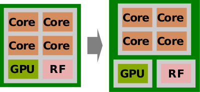
Chiplets refer to the independent constituents which make up a large chip built out of multiple smaller dies. Historically the need to go with multiple chips was driven by the reticle limit which dictated the maximum size of chip possible to be fabricated. Designs that exceeded the reticle limit had to be split up into smaller dies in order to be manufacturable. As process technologies continued to enable higher integration, multiple dies were merged into single, more complex integrated circuits. More recently, economics has resulted in a reversal of that trend. The desire to move to a chiplet-based designed has been driven by the increasing cost of manufacturing devices on leading-edge process nodes. Due to the cost associated with leading-edge nodes, it became advantageous to, once again, de-integrate and break down a large die into smaller 'chiplets' in order to improve yield and binning.
Motivation
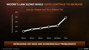
As the industry moves to smaller process nodes, costs for yielding large dies continues to increase. Compared to 250 mm² die on the 45 nm process, the 16 nm process more than doubles the cost/mm² and the 7 nm process nearly double that to 4x the cost per yielded mm². Moving to the 5 nm and even 3 nm nodes, the cost is expected to continue to increase. Fabricating large monolithic dies will becomes increasingly less economical. One solution to easing the economics of manufacturing chips with a large amount of transistors, the industry has started shifting to chiplet-based design whereby a single chip is broken down into multiple smaller chiplets.
Example
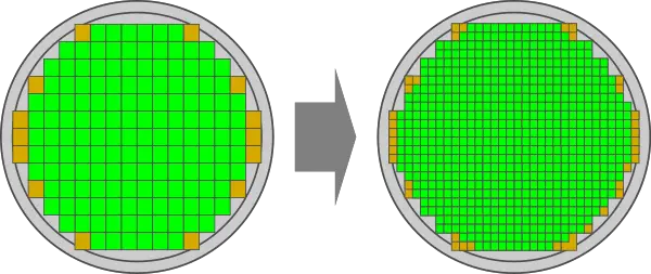
Consider a D0 of 0.1 defects per cm². Now, consider a medium-sized die 18 mm x 20 mm (360 mm²). On a standard 300-millimiter wafer size, up to 150 dies can be fabricated.
Splitting up the same die into four chiplets - 9.5 mm x 10.5 mm (~99 mm²) results in 622 dies instead.
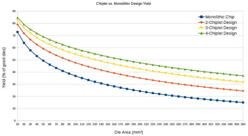
Below is a plot of percent of yield per wafer for a die of various sizes versus the same die consisting of two, three, and four chiplets. Note that an additional 10% overhead for the cross-die communication has been added to the chiplet-based design.
From the graph above, it can be seen that a 360 mm² monolithic die will have an yield of 15% while a 4-chiplet design (each 99 mm²) more than doubles the yield to 37%. The total die area of the 4-chiplet design incurs a ~10% area penalty (36 mm² for a combined silicon area of 396 mm²) but the significant improvement in yield which directly translates to lower cost more than justifies this.
Challenges
| This section is empty; you can help add the missing info by editing this page. |
Technologies
Packaging
Interconnect
This list is incomplete; you can help by expanding it.
Bibliography
- IEDM 2017, Dr. Lisa Su. Keynote presentation.


